
Xiaowei WU, Jiayan LI. Texturing Technology on Multicrystalline Silicon Wafer by Metal-catalyzed Chemical Etching: a Review [J]. Journal of Inorganic Materials, 2021, 36(6): 570
- Journal of Inorganic Materials
- Vol. 36, Issue 6, 570 (2021)
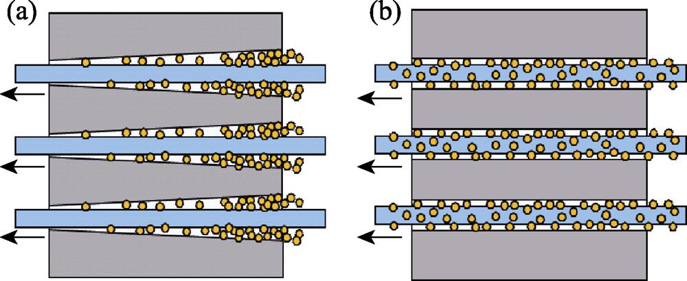
1. Schematic diagram of (a) MWSS cut technique and (b) DWS cut technique
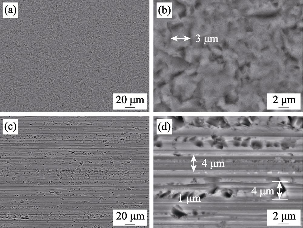
2. SEM images of (a, b) MWSS cut and (c, d) DWS cut multicrystalline silicon wafer surface
3. Surface SEM morphology and reflectivity for texture surface of silicon wafer by acid etching
4. Schematic diagram of MCCE[18]
5. SEM images of silicon surfaces with (a) nano-texture, (b) micro-texture and (c) nano-micro-texture[31]
6. (a) Schematic illustration of the main steps to prepare the submicron-in-micron (SIM) texture on the DWS mc-Si wafer and (b) experimental reflectance (curves) and simulated reflectance (scatter points) of three samples[33]
7. Surface and cross-sectional SEM images of mc-Si grains after etching by alkali, Ag-MCCE and post-etching with different orientations[34]
8. SEM images of Si nanostructures produced by Cu-MCCE method (a,b) before and (c,d) after the post-processing treatment and (e) schematic diagram of post-processing treatment[41]
9. Cross-sectional SEM images of Si wafers after (a) Ag-MCCE and (b) Cu-MCCE, and (c) schematics of etching process by single Cu- and Ag-catalyzed chemical etching and Ag/Cu-cocatalyzed chemical etching[45]
|
Table 1. Performances for texture surfaces of DWS cut multicrystalline silicon prepared via different MCCE methods
|
Table 2. Comparison of making texture surface on DWS cut multicrystalline silicon by different MCCE methods


Set citation alerts for the article
Please enter your email address

© Copyright 2018-2021 | Chinese Laser Press. All Rights Reserved 沪ICP备15018463号-20