• Acta Optica Sinica
  • Vol. 40, Issue 20, 2001001 (2020)
Jingjing Shi1、2, Yadong Hu2、*, Mengfan Li2, Bin Sun2, Gai Wang2, Gaojun Chi2, Xiangjing Wang2, and Jin Hong1、2
Author Affiliations
  • 1School of Environmental Science and Optoelectronic Technology, University of Science and Technology of China, Hefei, Anhui 230026, China
  • 2Anhui Institute of Optics and Fine Mechanics, Chinese Academy of Sciences, Hefei, Anhui 230031, China
  • show less
    DOI: 10.3788/AOS202040.2001001 Cite this Article Set citation alerts
    Jingjing Shi, Yadong Hu, Mengfan Li, Bin Sun, Gai Wang, Gaojun Chi, Xiangjing Wang, Jin Hong. Design and Implementation of Cloud Camera Control System[J]. Acta Optica Sinica, 2020, 40(20): 2001001 Copy Citation Text show less
    Block diagram of cloud camera electronics system
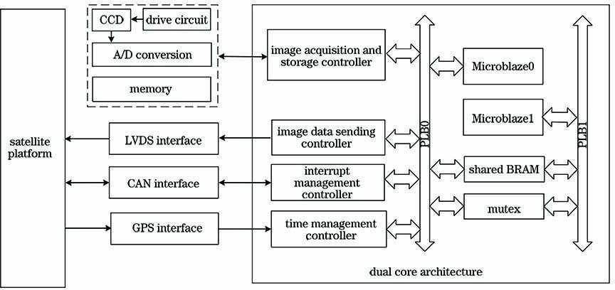
    Fig. 1. Block diagram of cloud camera electronics system
    Three-level pulse signal driving circuit
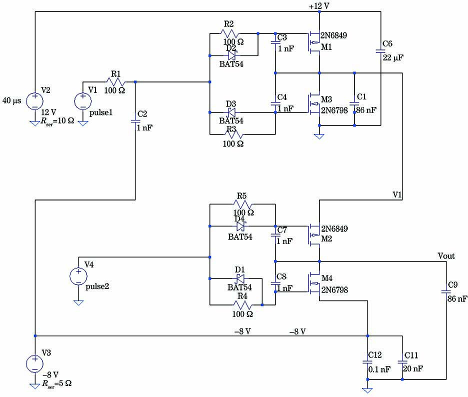
    Fig. 2. Three-level pulse signal driving circuit
    Simulation diagram of three-level pulse signal
    Fig. 3. Simulation diagram of three-level pulse signal
    Driving circuit of electronic shutter
    Fig. 4. Driving circuit of electronic shutter
    Frame transfer timing, pixel readout timing, and electronic shutter timing. (a) Frame transfer timing; (b) pixel readout timing; (c) electronic shutter timing
    Fig. 5. Frame transfer timing, pixel readout timing, and electronic shutter timing. (a) Frame transfer timing; (b) pixel readout timing; (c) electronic shutter timing
    Vertical clock, horizontal clock and reset signal,and electronic shutter. (a) Vertical clock; (b) horizontal clock and reset signal; (c) electronic shutter
    Fig. 6. Vertical clock, horizontal clock and reset signal,and electronic shutter. (a) Vertical clock; (b) horizontal clock and reset signal; (c) electronic shutter
    SDRAM initialization process, and diagram of working state transition. (a) SDRAM initialization process; (b) diagram of working state transition
    Fig. 7. SDRAM initialization process, and diagram of working state transition. (a) SDRAM initialization process; (b) diagram of working state transition
    CCD data acquisition and storage IP core
    Fig. 8. CCD data acquisition and storage IP core
    Block diagram of performance test
    Fig. 9. Block diagram of performance test
    Camera performance test site
    Fig. 10. Camera performance test site
    Measurement results of dark current noise
    Fig. 11. Measurement results of dark current noise
    Relationship between output signal value and exposure time
    Fig. 12. Relationship between output signal value and exposure time
    DescriptionSignalLevelVoltageEquivalent capacitance /nF
    High12 V
    Vertical clockV1T/V1BMid0 V43
    Low-8 V
    V2T/V2BHigh0 V
    Vertical clockV3T/V3BLow-8 V43
    V4T/V4B
    Horizontal clockH1Sα/ H2SαHigh0 V
    Low-5 V0.28
    Horizontal clockH1Bα/ H2BαHigh0 V
    Low-5 V0.19
    Horizontal clockH2SLαHigh0 V
    Low-5 V0.02
    Reset gateRαHigh3 V
    Low-2 V0.016
    Electronic shutterSUBHighVSET
    LowVSUB3
    Table 1. CCD drive signal levels and equivalent capacitances
    T /ms710152025303540506070
    SNR20.524.537.143.952.368.374.776.8102.2113.8128.1
    Table 2. Camera SNR at different exposure time
    Jingjing Shi, Yadong Hu, Mengfan Li, Bin Sun, Gai Wang, Gaojun Chi, Xiangjing Wang, Jin Hong. Design and Implementation of Cloud Camera Control System[J]. Acta Optica Sinica, 2020, 40(20): 2001001
    Download Citation