
Yufeng Yang, Mingzheng Jiang, Ying Zhang, Huan Zhang. Design of Full Duplex Visible Light Communication System Based on Single Light Source[J]. Laser & Optoelectronics Progress, 2019, 56(1): 010603
- Laser & Optoelectronics Progress
- Vol. 56, Issue 1, 010603 (2019)
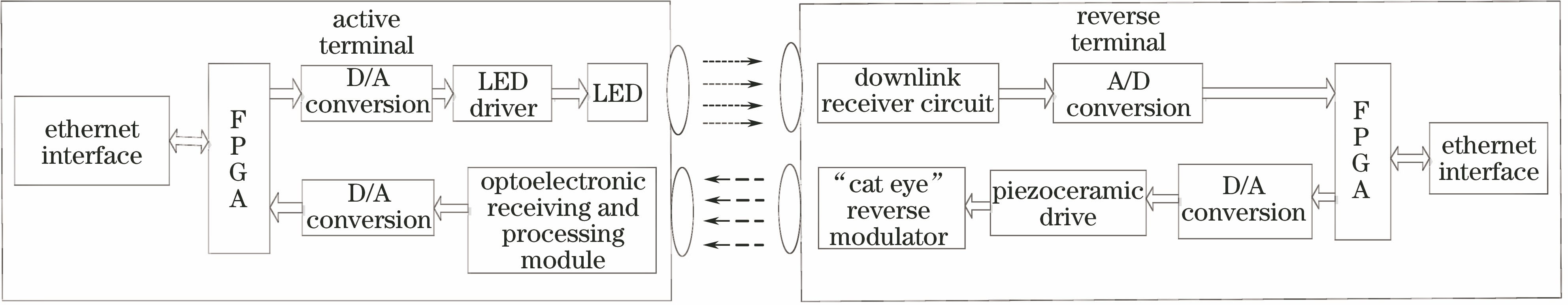
Fig. 1. Visible light full duplex communication system block diagram
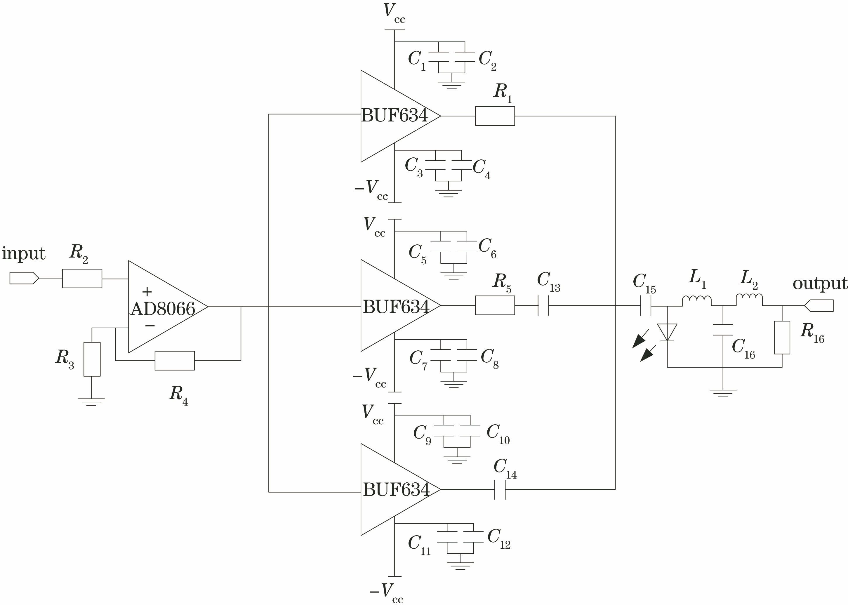
Fig. 2. Schematic of LED drive circuit
Fig. 3. Defocused model reverse modulator
Fig. 4. Cat eye reverse modulator principle diagram. (a) Non-focal type model reverse modulator; (b) defocused model reverse modulator
Fig. 5. Driving amplifier circuit module
Fig. 6. Active bandpass filter principle diagram
Fig. 7. Diagram of active terminal
Fig. 8. Diagram of reverse terminal
Fig. 9. LED driver circuit diagram. (a) PCB diagram; (b) module
Fig. 10. Photoelectric receiving circuit diagram. (a) PCB diagram; (b) module
Fig. 11. Hardware circuit test diagram. (a) LED drive circuit; (b) photoelectric receiving circuit
Fig. 12. Reverse modulator drive circuit diagram. (a) PCB diagram; (b) reverse drive circuit diagram
Fig. 13. Piezoelectric ceramic driver circuit test diagram
Fig. 14. System error rate test. (a) Downlink; (b) uplink
|
Table 1. Active terminal parameters
|
Table 2. Reverse terminal parameters

Set citation alerts for the article
Please enter your email address
© Copyright 2018-2021 | Chinese Laser Press. All Rights Reserved 沪ICP备15018463号-20