
Lei Lei, Fei Lou, Keyu Tao, Haixuan Huang, Xin Cheng, Ping Xu, "Tunable and scalable broadband metamaterial absorber involving VO2-based phase transition," Photonics Res. 7, 734 (2019)
- Photonics Research
- Vol. 7, Issue 7, 734 (2019)
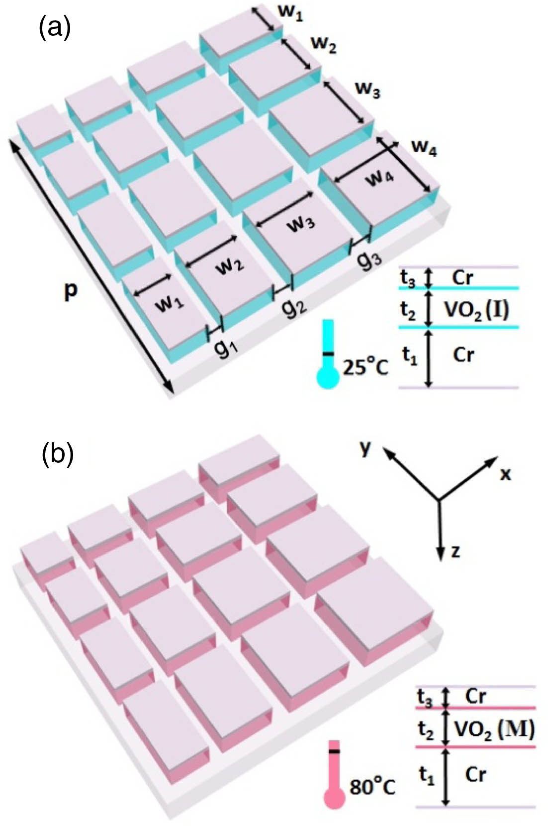
Fig. 1. Schematic diagrams of the tunable and scalable metamaterial ultra-broadband absorber with the VO 2 Cr − VO 2 p = 1900 nm w 1 = 200 nm w 2 = 300 nm w 3 = 400 nm w 4 = 500 nm t 1 = 300 nm t 2 = 260 nm t 3 = 30 nm g 1 = 80 nm g 2 = 120 nm g 3 = 140 nm
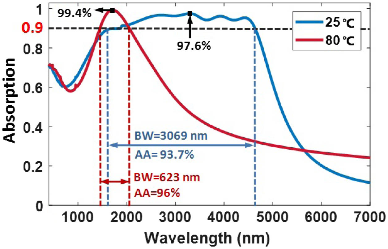
Fig. 2. Calculated absorbance spectra. BW, bandwidth; AA, average absorption.
Fig. 3. Electric and magnetic field distributions of the TSMA with the VO 2
Fig. 4. Electric and magnetic field distributions of the TSMA with the VO 2
Fig. 5. (a), (b) Spectral comparison between the proposed TSMA and planar films with different top metals. (c), (d) Spectral comparison between TSMAs with different top and bottom metals.
Fig. 6. (a) Real parts of the refractive indices for Cr and VO 2 VO 2 VO 2
Fig. 7. Scalability demonstration of the VO 2
Fig. 8. Absorption spectra of the VO 2 VO 2
Fig. 9. Angular dispersions of the TSMA under VO 2 VO 2


Set citation alerts for the article
Please enter your email address

© Copyright 2018-2021 | Chinese Laser Press. All Rights Reserved 沪ICP备15018463号-20