Optical absorbers with dynamic tuning features are able to flexibly control the absorption performance, which offers a good platform for realizing optical switching, filtering, modulating, etc. Here, we propose a thermally tunable broadband absorber applying a patterned plasmonic metasurface with thermo-chromic vanadium dioxide () spacers. An actively tunable absorption bandwidth and peak resonant wavelength in the region from the near- to mid-infrared (NMIR) are simultaneously achieved with the insulating–metallic phase transition of . Moreover, the scalable unit cell, which is composed of multi-width sub-cells, provides a new freedom to further manipulate (i.e., broaden or narrow) the absorption bandwidth while maintaining a high relative absorption bandwidth and efficient absorbance at the same time. For both transverse-electric and transverse-magnetic polarizations, the proposed nanostructure exhibits a high absorption over a wide angular range up to 60°. This method holds a promising potential for versatile utilizations in optical integrated devices, NMIR photodetection, thermal emitters, smart temperature control systems, and so forth.
1. INTRODUCTION
Metamaterial nano-structures are able to be designed to yield a desired permittivity or permeability. Thus, by tailoring the size and geometry of nanostructures, spectral engineering, phase manipulation, and polarization control can be flexibly achieved. This characteristic makes metamaterial a promising way for various and wide applications such as light harvesting [1,2], imaging [3], ultra-sensitive sensing [4], polarization conversion [5,6], filtering [7,8], ultra-short pulse generation [9,10], optical angular momentum generation [11,12], and many more processes, among which, controlling and engineering the spectral absorption properties of optical metamaterials has attracted huge interest in recent years. In particular, metamaterial and plasmonic absorbers have been demonstrated to realize either narrow or broadband absorption over microwave [13], terahertz [14], visible [15], and infrared [16] bands.
Besides the absorbers with fixed absorption performances, those with dynamic control features arouse an increasing interest since they open up applications in integrated devices such as modulators [17,18] and optical switching [19,20]. This is not only motivated by intrinsic research interest; the dynamic absorptive metamaterial also exhibits highly useful applications in our daily life and in spacecraft. The thermal controlling mechanism enables a low emittance at low temperatures to keep the heat and a simultaneous high emittance at high temperatures to dissipate surplus heat, giving rise to developments in smart windows [21,22] and smart solar reflectors [23].
An efficient way to implement thermal controlling is to employ phase change materials, among which, vanadium dioxide () is an ideal material due to its thermochromic characteristic of undergoing a transition from insulator to metal at a critical temperature of around 68°C [24]. During this transition, the lattice is transformed from a monoclinic to tetragonal structure as the temperature rises. Meanwhile, the conductivity of increases by several orders of magnitude, leading to dramatically changed optical and electric properties of the related materials or devices [25–29].
Sign up for Photonics Research TOC. Get the latest issue of Photonics Research delivered right to you!Sign up now
In this work, we propose a thermally tunable broadband absorber with patterned metal plasmonic metasurface with thermo-chromic vanadium dioxide () spacers. Actively tunable absorption bandwidth and peak resonant wavelength are simultaneously achieved spanning from the near- to mid-infrared (NMIR) with the insulating–metallic phase transition of . Specifically, an ultra-broadband absorption over the range of 1627–4696 nm is successfully achieved under the insulating state. The 90% relative absorption bandwidth () reaches to 97% with an average absorption higher than 93.5%. Electromagnetic field distributions reveal that multiple hybrid plasmonic resonant modes collectively lead to such a wide band absorption. Under the metallic state, the proposed absorber gains an increased average absorbance around 96% in the 90% absorption bandwidth () of 632 nm (i.e., 1443–2066 nm). More importantly, we further demonstrate that the absorption bandwidth can be further broadened or narrowed by correspondingly cascading or removing the multi-width sub-cells, which provides a new freedom to flexibly manipulate the absorption bandwidth while simultaneously maintaining high and average absorption. For both transverse-electric (TE) and transverse-magnetic (TM) modes, this plasmonic device maintains a high absorption over a wide range of incident angles up to 60°. Based on the features of dynamic thermal tuning and configuration scalability, our design is evidently beneficial to versatile applications such as optical modulators, optical switching, NMIR photodetection, thermal emitters, and smart temperature control systems.
2. GEOMETRY AND METHODS
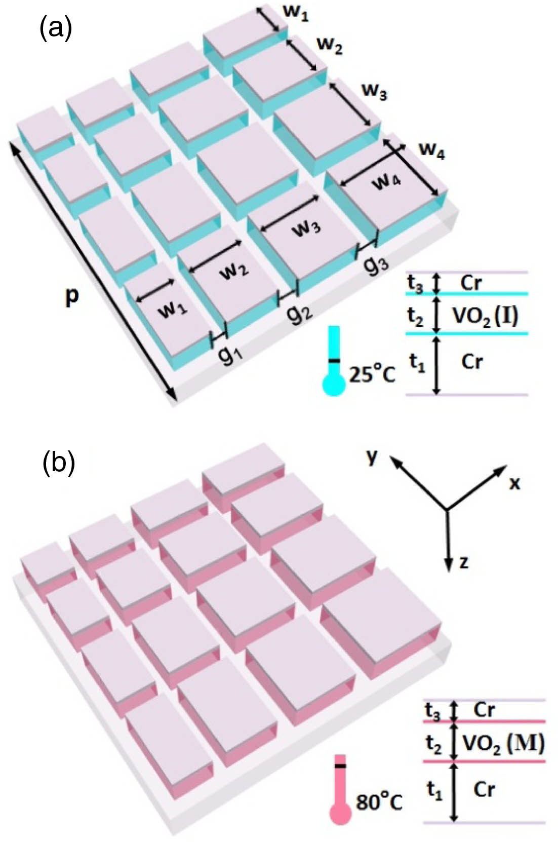
The tunable and scalable broadband metamaterial absorber (TSMA) presented here is composed of chromium (Cr) top caps, spacers, and a Cr film substrate, where the former two are tailored by the same pattern. As illustrated in Fig. 1, the unit cell contains a group of different sized cubes, of which each one is defined as a sub-cell. The period () of the unit cell is 1900 nm in both the and directions, which promises that the absorption resonance will be located at the NMIR band. A 2D-TSMA grating model with a single sub-cell is adopted to pre-design the proper widths of the sub-cells. With this preparatory width sweep, (200 nm), (300 nm), (400 nm), and (500 nm) are selected as the best candidates to enable a combined broadband absorption covering most of the NMIR region. In the 3D-TSMA model, sub-cells arrange in an order as , , , and in the positive direction, while in the positive direction the order reverses as , , , and .
Figure 1.Schematic diagrams of the tunable and scalable metamaterial ultra-broadband absorber with the spacer in the (a) insulating phase and (b) metallic phase. Here, a group of multi-width sub-cells is placed directly on the surface of a uniform Cr substrate. Parameters are set as , , , , , , , , , , . The surrounding material is air.
Hence, we achieve square cube nano-antennas on the main diagonal and rectangular ones in the rest. The thicknesses of the Cr−VO2−Cr layers from top to bottom are 30 nm (), 260 nm (), and 300 nm (), and the gaps between the columns are 80 nm (), 120 nm (), and 140 nm (). As shown in Figs. 1(a) and 1(b), the spacers behave like insulators at room temperature of 25°C, while fully transitting to metallic phase in a hot environment at 80°C. We correspondingly refer to these two different device conditions as (I) and (M). The critical phase transition temperature of in our study is set as 68°C. The optical constants of in both the insulating and metallic phases are fitted to the data reported in Ref. [24], where the permittivity from visible to 2.25 μm is experimentally measured by variable angle spectroscopic ellipsometry, and the permittivity from 2.25 to 8 μm is then fitted by the Tauc–Lorentz model [ (I)] and Drude model [ (M)]. The permittivity of Cr used in our simulations is fitted according to the data reported in Ref. [30]. As to the fabrication of the proposed structure, the film can be coated by pulsed laser deposition [31], magnetron sputtering deposition [32,33], or chemical vapor deposition [20]. For patterning the Cr−VO2 nanostructures, we can first use a metal liftoff process to fabricate the Cr nano-cubes by electron beam lithography or nano-imprint lithography, and then the Cr nano-cubes can be employed as the hard mask for plasma etching [24].
The resonant responses are modeled by the method of three-dimensional finite-difference time-domain (FDTD). We set periodic boundary conditions for the lateral boundaries ( and axes) and perfectly matching layers (PML) along the direction to eliminate the boundary scattering. The reflection spectrum is recorded by a 2D frequency-domain power monitor that is placed behind the incident source. The Cr film substrate is thick enough to well block the incident light, and the transmission () of the structure is nearly zero (), resulting in the absorption (reflection). Electric and magnetic fields are monitored by the frequency profile monitors.
3. RESULTS AND DISCUSSION
A. Absorption Performance and Principles
The absorption spectra of the proposed TSMA applying are illustrated in Fig. 2. At room temperature around 25°C, the spacers work as a dielectric, and thus the absorber performs as a metal/dielectric/metal structure, which enables an ultra-broadband continuous high absorption with a 90% absorption bandwidth () wider than 3 μm (i.e., 1627–4696 nm), covering from the near- to mid-infrared. The average absorbance over this band is in excess of 93.5%. The corresponding relative absorption bandwidth (), expressed as , where and denote the respective long and short limits of the 90% absorption bandwidth, is higher than 97%. Nearly perfect absorbance is achieved from 3173 to 3404 nm with a peak absorption of 97.6% at 3297 nm. As the temperature increases, transits into the metallic phase so the device becomes an all-metal metamaterial structure at 80°C. In this case, the all-metal configuration dramatically depresses the multiple resonant modes in the vertical direction but enables stronger transverse resonances, which are spectrally closed. Hence, the absorption bandwidth turns into a relatively narrower range from 1443 to 2066 nm, indicating the of 623 nm. However, compared to the performance of the (I) nanostructure, the average absorbance in this case increases to 96%, and the resonance peak simultaneously grows to 99.4% around 1706 nm.
Figure 2.Calculated absorbance spectra. BW, bandwidth; AA, average absorption.
To investigate the underlining physical mechanism of the TSMA, electric and magnetic field distributions ( and ) are scrutinized under normal incidence at the specific resonant wavelengths. The electromagnetic field distributions of the insulating and metallic -TSMAs in the − plane are illustrated in Fig. 3 and Fig. 4, respectively. As apparently displayed in Figs. 3(a)–3(e) and Fig. 4(a), the electric fields are mainly confined in the grooves; this is attributed to the surface plasmon polaritons (SPPs), which are excited in the metamaterial structure so that light is mainly coupled into the air slot and localizes around the metal corners between the adjacent sub-cells, creating an SPP-induced light absorption. Figures 3(b)–3(e) also reveal the relationship between the sub-cells and resonant wavelengths so that the resonant wavelength is accordingly red-shifted as the width of the sub-cell increases. This scalability feature of the TSMA is greatly beneficial to the absorption bandwidth. In specific, apart from the existing sub-cells, the absorption bandwidth can be easily broadened by applying additional larger sub-cells. This multi-width distribution enables a new freedom to achieve an ultra-wideband absorption. Compared to the electric field distributions, the magnetic fields exhibit intrinsically different profiles. As to Fig. 3(f), the resonance is supposed to be the propagating surface plasmon (PSP) resonance between the continuous Cr substrate and spacers, where the magnetic field is not only strongly confined around the interface underneath the nano-cubes but also intensively enhanced between the adjacent sub-cells. In addition, we see the magnetic field extends far away from the surface due to the effect of the Rayleigh–Wood anomalies (RAs) [34]. Such anomalies lead to a spectral passing-off of high order. In other words, a diffracted wave arises and propagates tangentially to the surface of the periodic nanostructure at a certain wavelength. Also, such anomalies do not depend on the material of the nanostructure but instead on the period of the incident wavelength and the refractive indices of the surrounding media. This phenomenon is described by the well-known grating formula , where, and respectively denote the angular frequency and incident angle of the incident light, is an integer that defines the diffraction order, and refers to the period of the unit cell. It is seen from the equation that RAs’ wavelength is closely related to the period () of the unit cell, resulting in the slight absorption peak around 1900 nm as shown in Fig. 2. For Figs. 3(h)–3(j), localized surface plasmon (LSP) resonances at the longer wavelengths of 3297, 3910, and 4447 nm primarily dominate the absorption so that the magnetic fields are mainly localized within the spacer. On the other hand, the incident light penetrates through the thin Cr cap and bounces back at the Cr substrate layer. These two reflectors together with the spacer compose a lossy Fabry–Perot (FP) cavity with a low factor, resulting in the FP resonance-induced wideband light absorption. As a result, the magnetic distribution of the peak at 2704 nm illustrated in Fig. 3(g) corresponds to a hybrid mode, which involves PSP, RAs, LSP, and FP modes.
Figure 3.Electric and magnetic field distributions of the TSMA with the under the insulating state.
In the situation, it is evident that both the electric and magnetic fields are strongly concentrated in the air gaps. The resonance oscillates as a magnetic dipole, which can be seen from the confined magnetic field in the gaps. A transverse FP cavity of is formed by the sub-cells, and the air gap acts as the dielectric layer. With the help of the Cr film, this resonance can be well excited. Hence, due to the relatively poor scattering ability of the magnetic dipole resonance in the deep subwavelength region, we can attribute the narrower band perfect absorption to the transverse gap SP and FP modes.
The intensive absorption enhancement induced by the SPP modes is then numerically demonstrated in Figs. 5(a) and 5(b) by comparing the absorption spectra of the proposed TSMA (solid lines) with those of the planar films (dashed lines). As a reference, the layer thicknesses of the planar film configurations are correspondingly identical to those of the TSMA. Apart from Cr, we replace the topmost metallic film to different common metals including aluminum (Al), tungsten (W), and nickel (Ni), which provide high absorption in the visible, near-infrared, and mid-infrared. Besides, they also have a wide usage in absorbers and thermal emitters [35–37]. It is found that under either low or high temperature, the proposed TSMA exhibits an apparently stronger absorption and wider absorption bandwidth compared to those of the planar films due to the SPP enhancement. Specifically, we observe from Fig. 5(a) that the average absorption of our structure over 1.6–4.6 μm is as high as 93.6%, that is, 40 times, 4.5 times, 3.8 times and 2.8 times higher than that of the planar Al, W, Ni, and Cr absorbers, respectively. In Fig. 5(b), the average absorption of the TSMA reaches 95% over 1.4–2.1 μm, exhibiting a corresponding 39-time and 2.8-time enhancement to the planar Al and Cr absorbers and a 4.4-time enhancement to either W or Ni absorbers. These results in turn further demonstrate that the hybrid resonance modes, including PSP, LSP, RAs, and FP, together contribute to the optimal absorption performance. Additionally, we compare the absorption capability of the TSMA structures with different top and bottom metals as shown in Figs. 5(c) and 5(d). One can see that when replacing Cr with common plasmonic metals like Al, the spectrum under (I) state exhibits notable ripples in a wide wavelength range. The reason is that Al is less lossy than Cr, and thus the resonant cavities of the Al-TSMA have higher factors. Correspondingly, the combination of these resonances with narrower bandwidths exhibits notable ripples. For a lossy metal such as W or Ni, the TSMA also promises similar spectral performance. However, Cr-TSMA exhibits the best spectral performance in the aspects of absorptance, bandwidth, and flatness as well. Moreover, Cr is applied in our configuration also because of its high melting point, erosion resistance, and low cost.
Figure 5.(a), (b) Spectral comparison between the proposed TSMA and planar films with different top metals. (c), (d) Spectral comparison between TSMAs with different top and bottom metals.
The temperature dependence of dielectric permittivity is expressed as where and respectively refer to the dielectric permittivity of the insulating and metallic phase, and is a temperature-dependent function that is in charge of the distributions of insulating and metallic optical properties [38]. Here, is described as where is regarded as the real-time temperature, denotes the phase transition critical temperature, and is a variable controlling the width of the transition. It is noted that this function owns a Fermi–Dirac-like distribution that governs the energy states in thermodynamic distributions. Figures 6(a) and 6(b) plot the refractive indices of Cr and at different temperatures. It is noted that the refractive index of Cr is assumed to be insensitive to the temperature because it is a refractory metal. One can see that when temperature is well below the phase transition point , behaves consistently as a low-loss dielectric, while as temperature reaches and beyond, transforms gradually to a highly lossy metal.
Figure 6.(a) Real parts of the refractive indices for Cr and . (b) Imaginary parts of the refractive indices for Cr and . (c) Temperature-dependent absorption spectra of the -based TSMA.
Figure 6(c) shows the spectral evolution during the heating process. At room temperatures from 25°C to 40°C, we achieve a wide absorption band greater than 3 μm. As the temperature increases, the absorption bandwidth gradually decreases to about 20% at 70°C when the is phase changed to its metallic state. Meanwhile, the peak absorption wavelength correspondingly blue-shifts from 3297 to 1706 nm. These thermal dynamic characteristics offer a flexible tuning, modulating, and switching behavior in absorbance.
More generally, by removing or cascading multi-width sub-cells in the proposed manner, our structure enables a flexible and efficient way toward the ultra-broadband absorber with reconfigurable absorption bandwidth while simultaneously maintaining high absorption. To demonstrate the configuration scalability, Fig. 7 illustrates the absorption spectra of the -TSMAs with unit cells containing 3-width, 4-width (i.e., the proposed structure), and 5-width sub-cells. Compared to the geometry of the 4-width structure, the 3-width one removes the cubes with the width of (500 nm), while the 5-width one cascades several cubes with the width of 600 nm and the air gap of 160 nm. In other words, and for the 3-width TSMA; , , , and for the 5-width TSMA. Taking the absorption spectrum of the 4-width configuration as a reference, it is clearly seen that in the insulating mode [Fig. 7(a)], the absorption bandwidth of the 3-width structure obviously compresses, while the 5-width configuration exhibits a notable broadening. This bandwidth reconfiguration greatly depends on the resonant mode primarily excited by the relative sub-cells with the largest width, but it is also the hybrid resonant modes together lead to the broadband absorption as aforementioned in Section A. Here, the respective 90% absorption bandwidths of the 3-width and 5-width structures are measured as 2495 and 3688 nm, corresponding to a relative absorption bandwidth of 88.7% and 105.1%. The average absorptions are still as high as 95.4% and 91.4%, respectively. Compared with the reported broadband absorbers in the NMIR range [39–41], our approach exhibits appealing characteristics in terms of simultaneous high relative absorption bandwidth, efficient average absorbance, scalable and simple pattern, and feasible fabrication process.
Figure 7.Scalability demonstration of the -TSMA with 3-width (black line) and 5-width (blue line) sub-cells, compared with the proposed reference structure with 4-width sub-cells (red line).
In addition, we also study the absorption spectra of the rescaled structures under metallic mode in Fig. 7(b). In this case, the absorption of the all-metal structure mainly originates from the transverse gap SP and FP resonances in the metal/air/metal cavities.
The FP resonance is given by , where is the air gap size and is the effective refractive index of the gap SP. A smaller ensures a more compact mode concentration, implying a larger , and vice versa. Accordingly, the resonance is nonlinearly related to the gap size. Thus, based on the combination of the multiple FP resonances, the absorption spectra turn out to be relatively consistent for the 3-width, 4-width, and 5-width configurations.
C. Geometry Influence on the Absorption Performance
To further explore the influence of geometry on the absorption performance, we calculate the absorption spectra with various thicknesses of the top Cr caps and spacers at 25°C and 80°C. In these simulations, , , , , and remain the original lengths. Figure 8(a) shows the absorption evolution depending on the thickness of the top Cr. The results are greatly sensitive to the top Cr thickness when works as an insulator. It is seen that the optimal performance is achieved around the top Cr of 30 nm, and the absorption bandwidth gradually decreases either as the Cr thickness increases or decreases. The reason is that a thinner Cr cap promises a less lossy cavity, while a thicker one indicates a weaker coupling. Thus, in both cases, the absorber suffers from the limitations of the absorbance as well as the bandwidth. The spectral evolution based on the variation of thickness, shown in Fig. 8(c), exhibits a similar performance to Fig. 8(a). As the spacer thickness directly determines the effective cavity length of the vertical cavity, the absorption band gradually red-shifts as thickness increases. However, the spectral evolution map is intrinsically different in the metallic model. In this case, the TSMA is regarded as an all-metal structure, and thus the influence of the Cr cap thickness is similar to that of the metallic . In both Figs. 8(b) and 8(d), resonance red-shifts are observed as the corresponding thickness increases. This is because the larger portion of light energy would be confined in the metals as the metals get thicker. Correspondingly, the effective refractive index () of the transverse gap SP and FP resonances is enhanced, resulting in a red-shift of the absorption spectra.
Figure 8.Absorption spectra of the -TSMA with various thicknesses of top-Cr and , calculated at 25°C and 80°C.
In Fig. 9, angular dispersions of the TSMA under (I) as well as (M) phase are studied at various incident angles for both TE and TM modes. For the TE polarization, the TSMA exhibits nearly angle-independent spectral performance in a wide range of incident angles (i.e., 0°–60°). However, for the TM polarization, the absorption degrades as the incident angle increases. This polarization-dependent angular dispersion of the TSMA can be explained by the direction of the magnetic field. Specifically, the magnetic field direction of the TE-incident light remains unchanged as the incident angle varies, which efficiently drives the circulating currents at all oblique incidences. On the contrary, for the TM polarization, the magnetic field rotates with regard to the variable incident angles. As a consequence, the circulating currents cannot be driven that efficiently, especially at large-angle incidence. Nevertheless, the average absorptances from 1600 to 4600 nm under the (I)-TM condition at 40° and 60° still exceed 87.5% and 70.3%, respectively.
Figure 9.Angular dispersions of the TSMA under (I) as well as (M) for both TE and TM polarizations.
In summary, we propose a unique strategy for dynamic broadband absorption in the range from the near- to mid-infrared with a -based metamaterial structure. Through the highly efficient utilization of multiple resonant modes in the -based metamaterial absorber, we simultaneously achieve thermally tunable absorption bandwidth and resonant wavelengths. The 90% absorption bandwidth changes from 3069 to 632 nm as transits from an insulating to metallic state, and the respective average absorptions over the corresponding bands are as high as 93.5% and 96%. The physical mechanism has been clearly explained by the electromagnetic field distributions and spectral comparison between the TSMA and planar film absorbers with different topmost metals. This wide-angle structure not only shows the evident advantage of flexible thermal tuning but also the capability of a scalable configuration, which provides a new freedom to further manipulate (i.e., compress or broaden) the absorption bandwidth and meanwhile maintains a high relative absorption bandwidth and efficient average absorption. Apart from the traditional applications such as thermal emitters, photodetectors, optical modulators, and filters, this design shows a great prospect in developing smart nanostructures or devices such as smart glass, smart temperature control systems, and smart solar reflectors.
Acknowledgment
Acknowledgment. The authors thank Professor Dongping Zhang at Shenzhen University for the very helpful discussion on VO2 fabrication. We also thank our group members Junhang Zhang, Songrong Xu, Longzhan Huang, Zeye Xu, and Junyan Huang for the supplementary simulation on angular dispersions.