
Senpo Yip, Lifan Shen, Johnny C Ho. Recent advances in flexible photodetectors based on 1D nanostructures[J]. Journal of Semiconductors, 2019, 40(11): 111602
- Journal of Semiconductors
- Vol. 40, Issue 11, 111602 (2019)
Abstract
1. Introduction
In the past few decades, the development of semiconductor devices has reshaped our lifestyle. One of the major advancements is the development of sensor that can response with the change of the environment. Among different types of sensors, photodetector is an optoelectronic device that transform light signal to electric signal. Upon the illumination of a light source, the electricity passes through the photodetector changes. Photodetector has found applications in different categories, from flame and smoke detection[
In general, photodetectors are built on rigid substrate like bulk silicon. The limitation of the rigid photodetector is that when undergo even a small deformation, the photodetector will crack and cannot function properly. Also, rigid sensor cannot be used on curved surface and hence restrict the usage in certain area like body temperature monitoring[
A photodetector is typically constructed with a photosensing channel and two electrodes at the both ends of the channel. The sensing materials can be a bulk film or nanostructures like nanosheets, nanowires (NWs), nanotubes (NTs) or quantum dots (QDs). Among them, the 1D nanostructures like NWs and NTs exhibit some special properties like large surface-to-volume ratio that can enhance the photoresponse compare to their bulk counterparts. Also, due to the low dimensional feature, 1D nanostructure can withstand larger bending without cracking compares to their bulk counterparts. These features make the 1D nanostructure one of the ideal candidates to be integrated into flexible photodetector. In recent years, there are various attempts to develop NW-based flexible photodetector, from the material selection, fabrication and assembly techniques, to device fabrication and integrating them into a more complicated system for potential real-life application. In this review, the recent progress of NW fabrication and assembly techniques for flexible electronics are first reviewed. After that, some recent research progress is presented based on different material groups. Then the reports on integration of the flexible NW photodetector to more complicated system are introduced.
1.1. Types of photodetector
Before reviewing the recent progress, the background information would be first introduced. Firstly, some common types of photodetector are briefly introduced here. Photodetector can be classified as three groups based on their working principles. They are:
a) Photoconductor type: in which the excessive free charges is generated by absorption of photons. Those excessive charges increase the overall conductivity of the photodetector channel. Usually composed by a semiconductor channel as the sensing materials and two ohmic contacts as the source and drain for charges transfer.
b) Photovoltaic type: in which a built-in electric field is existed within the photodetector without illumination. This can be done by building a p–n junction within the sensing channel or a Schottky barrier junction between the contact and the semiconductor interface. Upon the illumination, the built-in electric field separates the photo-induced electron–hole pair and hence the generation of photocurrent.
c) Photogating type: in which an electric field is generated under the illumination. There are two types of mechanisms for the photogating effect generation. One is the photo-induced charges are trapped by the defects and the other is trapped by the surface absorbates. The trapped charges act as a local gate and modulate the current flow along the photodetector upon the illumination.
Different types of photodetectors have their individual advantage for applications. For example, photovoltaic type can be used to constructed self-powered photodetector which can reduce the total weight of the sensing unit as no external power source is needed[
1.2. Figure of merits
Another important background information is the performance figure of merit for assessing the photodetector. With these figure-of-merits, the performance of different photodetector can be compared. There are several figure-of-merits that are frequently used for assessing photodetector and briefly introduced here.
Responsivity (R): Responsivity is a description of the efficiency of charge/voltage generation under illumination. It is the measured photocurrent or photovoltage divided by the power of the illumination source on the active area of the sensing material. It can be expressed as:
where I and V are photocurrent and photovoltage respectively, and P is the illumination source power.
External quantum efficiency (EQE): The EQE is the ratio of the total generated electron pairs which contribute the photocurrent and the total numbers of incident photons. The EQE can be expressed as:
where e is the elementary charge, h is Planck's constant, v is the frequency of incident light, c is the speed of incident light, and λ is the wavelength of incident light.
Response speed: Response speed is used to describe how fast a photodetector response upon the light illumination. It is usually described as two values: one is rise time and the other is the decay time. They are defined as the time used for the photocurrent to rise from 10% of the peak photocurrent to the 90% of the peak photocurrent for the rise time, and the time used for the photocurrent to drop from 90% of the peak photocurrent to the 10% of the peak photocurrent for the decay time.
Detectivity (D): Detectivity is used to describe the ability to detect signal from noise. It can be expressed as:
where q is the light intensity and Idark is the dark current of the photodetector.
2. NW growth and assembly method for flexible electronics
2.1. Nanowire growth method
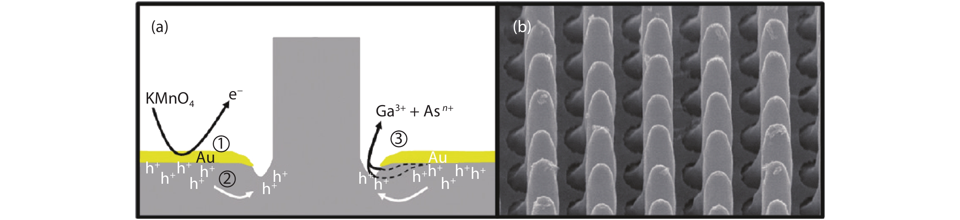
This part of the review will briefly introduce some NW fabrication techniques. Each technique has its own advantages and disadvantages. Basically, NW fabrication can be divided into two major categories, namely the “top–down” and the “bottom-up” approaches. The top–down approach means the NWs are fabricated from bulk materials and thin down the sizes and dimensionality. It is a simple and relatively straightforward method that involves material removal from a thin or thick film. Patterning is needed prior to the NW synthesis in order to define the NW position, shape and dimension. Material removal is performed by chemical etching or plasma etching. One example is metal-assisted chemical etching (MacEtch), which uses a patterned metal film as the catalyst to etch the substrate isotropically in order to create a high aspect-ratio structure[
![]()
Figure 1.(Color online) (a) Schematic illustrations of the formation mechanism of GaAs NWs. (b) SEM images of high aspect ratio GaAs NW produced from a 600 nm wide square Au mesh pattern in H2SO4 and KMnO4 solution at 40–45 °C. Reprinted from Ref. [
Bottom–up approach refers to the synthesis of NWs by employing their constituent atoms that grow anisotropically along the axial direction to obtain 1D single-crystalline structure. The ‘vapor–liquid–solid’ (VLS) method is a typical growth scheme that promotes seeding and oriented growth by introducing a catalytic liquid alloy phase, which can rapidly adsorb the vapor-phase precursor source to the supersaturation level, and then induce the precipitation of NWs and producing various types of semiconductor materials in a relatively large quantity[
Among all these methods, the VLS mechanism is most widely used in the growth of NWs due to its simplicity and versatility. Various techniques have been adopted to generate vapor-phase precursors, for example, by decomposition of the semiconductor reactants in chemical vapor deposition (CVD)[
Solution-mediated wet-chemical approaches are widely used for NWs growth due to the relative simplicity and economical potential[
![]()
Figure 2.(Color online) Illustration depicting the growth mechanism of a MAPbI3·DMF NW by in situ monitoring with an UV−Vis microspectrometer. Reprinted from Ref. [
2.2. Assembly method for flexible electronics
In the previous section, some NW fabrication techniques is introduced. To integrate them into photodetector, special transfer and assembly method in a controllable manner is crucial especially for flexible devices. For single NW devices, the NWs are randomly distributed on substrate by drop-casting method. However, it’s impossible to adopt this method with random and disordered NWs for large scale device arrays and mass production. For the fabrication of flexible NW detectors, typically there are two approaches: direct NW growth on flexible substrates and NW transfer to flexible substrates by different methods such as electrospinning method, contact printing, and peeling transfer method[
Recently, contact printing technique has attracted considerable attention, which can be utilized for large-scale assembly of NW parallel arrays on both rigid and mechanically flexible substrates followed by subsequent device fabrication. This approach can provide high performance and stable device operation at low cost[
![]()
Figure 3.(Color online) (a) Schematic of the process flow for contact printing of nanowire arrays. (b) Dark-field optical and (c) SEM images of Ge NWs (
As expected, the contact printing process can also be widely adopted for various semiconductor NWs, such as InAs, InGaAs and InGaSb NWs[
Spray coating technique is a simple method for the deposition of highly ordered and aligned NW arrays on different substrates, including silicon, glass, metals, and flexible plastics with controlled density[
![]()
Figure 4.(Color online) Schematic of the spray-coating process that involves a direct transfer of NW suspension to the receiver substrates. (a) Schematic and scanning electron microscopy (SEM) image of the NW sample used in this study. (b) Schematic of the NW suspension. (c) Schematic of the assembled apparatus used in this study. (d) Schematic and optical microscopy image of Si NW spray-coated on the SiO
Electrospinning is a facile, cheap and efficient technology to fabricate randomly oriented NWs on certain substrates. During the electrospinning process, the precursor liquid forms a Taylor cone at first and then turns into a charged jet under high electrostatic voltage. The charged jet will be further elongated and thinned under electrostatic force and Coulomb repulsion during travelling from outlet of injector to collector. With simple modification, such as field assisted method[
![]()
Figure 5.(Color online) Schematic of two-step all-printable process and materials characterization. (a) Printing setup schematic. (b, c) Electrospinning ejection from the tailored cone apex. (d, e) Optical images of the as-printed electrospun ZnAc/PVA nanofibres with 5 and 10 mm spacing, respectively. (f) SEM image of an as-calcinated ZnO GNW. (g) Transmission electron microscopy image of a GNW. Reprinted from Ref. [
Most transfer methods make NWs positioned horizontally on the substrate and the initial NW orientation cannot be maintained. Recently, an alternative transfer method yielding vertical NWs has gained a broad interest, which is based on NW embedding in a polymer layer followed by mechanical peeling of the membrane[
![]()
Figure 6.(Color online) (a) Schematic representation of the fabrication steps: encapsulation in PDMS and peel-off of the membrane; deposition of the back metal contact; deposition of the top transparent contact composed of a silver nanowire mesh. (b) Bird’s eye view SEM image of the top surface of the detector. (c) Top view SEM image of an individual nitride NW contacted with silver nanowires. (d) Device photo illustrating its flexibility. Reproduced from Ref. [
3. Nanowire-based flexible photodetector
Based on the optoelectrical properties, there are different group of 1D nanostructures that are capable to be integrated into photodetector. In this section, the recent development of NW-based flexible photodetectors is reviewed based on different material groups.
3.1. Group IV materials
3.1.1. Carbon nanotube
Carbon nanotube (CNT) is one of many allotropes of carbon, which is an interesting family that have intriguing optoelectronic properties depends on their molecular dimensionality[
In recent years, lots of research input is focus on the IR sensing based on CNT-based flexible photodetector. One of many motivations of developing CNT-based IR detector is the possibility of working in room temperature. Traditionally, IR-detector based on InGaAs and HgCdTe shows very good performance. However, those good performance can only be achieved when they are sufficiently cooled[
Although pure CNTs film can be used as the sensing materials, to further improve the photodetector performance, CNT-based heterostructures are also frequently studied. For example, CNT/other carbon allotropes based heterostructures can enhance the IR sensing. In a research of Park et al., fullerene (C60) was deposited on a bilayer of semiconducting single-walled CNT (sc-SWCNT)[
Another frequently studied CNT hybrid system is CNT/polymer system. On rigid sample, polymer like electrically and thermally insulating polycarbonate[
![]()
Figure 7.(Color online) (a) Scheme of the PVA/CNT flexible photodetector. (b)
It is worth mentioning that, despite this review mainly focus on the 1D nanostructure as the sensing material in the photodetector, conductive CNT film-based electrode is also being developed for optoelectronic devices due to its mechanical flexibility and the transparency[
3.1.2. Silicon nanowires
The advancement of the morden technology is mainly due to the development of silicon processing technology. Silicon has been extensively used in computer chip, solar cell and sensors. While being one of the most abundant elements on earth, which make it more affordable, easy to dope and forming stable oxide are the main reasons why silicon is widely used in microelectronic industry. Traditionally, silicon is rigid and bulk which is not usable for wearable and foldable electronics. Creating the nanostructures of silicon changes mechanical properties drastically and enhance its flexibility, which allows it to be integrated into wearable and foldable electronics[
The NW form of silicon is studied for photodetector applications. As the maturity of silicon NW fabrication from both top-down and bottom-up approaches, the assembly of Si NW on flexible substrate can be done by different methods. For example, large scale of Si NWs can be fabricated by a cost-effective MacEtch method on a silicon substrate[
Recently, Hossain et al. integrated the a single-crystalline percolative Si NW to a transparent and flexible photodetector (Fig. 8(a))[
![]()
Figure 8.(Color online) (a) Schematic of the measurement setup of the flexible percolative Si NW photodetector; (b) The transient photocurrent of the photocurrent. (c) The rise time and decay time, (d) the photoresponse at different frequency, (e) time-dependent photocurrent and dark current when the photodetector is bent or flat, and (f) the photocurrent and dark current of the flexible percolative Si NW photodetector as a function of bending cycles. Reproduced from Ref. [
3.2. III–V nanowires
With the excellent electrical and optoelectrical properties, III–V NWs are the ideal candidates for next-generation electronics and optoelectronics[
Single III–V NWs were explored for flexible photodetector integration[
Some special device structures have been demonstrated on flexible GaN NW photodetector. For example, Zhang et al. demonstrated to integrate the vertical GaN/InGaN NW array on a polymer membrane for UVA detection[
![]()
Figure 9.(Color online) (a) Schematic and (b) the band diagram of the transfer process of the GaN NW/graphene sandwich photodetector. Reproduced from Ref. [
Overall, the research input for III–V NWs as the sensing materials for flexible photodetector is still in infancy and the existing reports mainly focus on nitride-based or phosphorus-based III–V materials, which are mainly for UV–Vis photodetection. In group III–V family, III–As and III–Sb usually has small bandgap that can be used for short-wave IR (1–2.5 µm), mid-wave IR (3–5 µm) to long-wave IR (8–12 µm) sensing[
3.3. Metal oxide nanowires
Metal oxide is one of the most studied materials for various applications, from sensing to electronic component, to heavy metal ions filtering[
Despite remarkable progress has been achieved, the NW photodetector constructed by homojunction NW as the sensing materials have a lot of setback compares to their heterostructure counterpart. Recently, more efforts are put into fabricating metal oxide NW heterostructures. Here on, some recent examples about flexible photodetector based on metal oxide NWs-based heterostructures are introduced.
Surface decorating the surface of metal oxide NWs with QDs is one approach to enhance the device performance. For example, decorating the Zn2SnO4 NWs with ZnO QDs can enhance photocurrent and responsivity[
![]()
Figure 10.(Color online) (a)
Recently, metal oxide NW photodetector integrated on fiber-like substrates attracts some research interest for the application in smart textile[
3.4. Metal chalcogenide nanowires
Chalcogenide NW is a group of NWs that contain S, Se or Te as their anions. Some of these materials have direct bandgap and as their bandgap lie in the visible light region which makes them potential candidate for optoelectronic that works in Vis region. Metal chalcogenide materials include some II–VI semiconductors (like CdS and SnS) and materials like Sb2S3 and In2S3. Their NW form are frequently used to be integrated into rigid substrate-based photodetector[
Cadmium based II–VI NW like CdS and CdSe NWs were integrated into flexible photodetector. Branched CdS NWs were fabricated by Li et al. which exhibit high detectivity on rigid substrate[
Recently, the III–VI NWs have shown some promising result for flexible photodetector integration. Single crystalline In2S3 NWs have demonstrated a high on-off ratio (106)[
3.5. Perovskite nanowires
Hybrid organic-inorganic are recently attracting tremendous amount of research interest for solar cell and photodetector[
The stability of perovskite material against the surrounding environment has been a concern. For flexibility photodetector, as it would under bending and continuous bending cycles, the stability issues become more important to be considered. There are various reports focusing on how to improve the stability of the organic–inorganic perovskite NW on flexible photodetector. For example, single-crystalline CH3NH3PbI3 NWs based photodetector can remain stable after 45 days of storage due to the high crystal quality of the NW produced by the saturated vapor-assisted crystallization method[
As the fabrication of perovskite can be done in low temperature, it can be directly fabricated on the flexible substrate without the need of transfer. Zhou et al. growing the perovskite NWs using micro/nanofluidic fabrication technique and integrated them into flexible photodetector.[20] Using a DMF-mediated crystallization method, the initial growth site and the growth path of the MAPbI3 NWs can be guided by a micro/nano fluidic channel on flexible substrate. Deng et al. fabricated the CH3NH3PbI3 microwires array on PET substrate using blade coating method. The microwires array fabricated by this method not only has good crystallinity but can also be stored over 50 days with only a mild fluctuation.
One recent report employed ferroelectric poly(vinylidene-fluoride-trifluoroethylene) (P(VDF-TrFE)) and hybrid perovskite NW to construct a flexible self-powered photodetector that is also semi-transparent[
![]()
Figure 11.(Color online) (a) The rise time and decay time and (b) the responsivity and detectivity curves of the perovskite NW photodetector at 0 V. Reprinted from Ref. [
Apart from the organic-inorganic perovskite NWs, pure inorganic NWs are also investigated for high performance photodetector due to the better stability[
4. System integration of NW-based flexible photodetector
So far, the recent developments of the NW-based flexible photodetector are reviewed. However, individual photodetector is not enough for imaging applications but to integrated large amount of photodetector into photosesning matrix. On the other hand, extra power source is always needed for photodetecting devices. To take the full advantage of the flexibility and compactness of the flexible photodetector, self-powered photodetector is also an important development. These two developments will pave the way for flexible photodetector integration for different applications.
4.1. Image sensor
Image sensing is an important application of photodetector. The ability of sensing different wavelength gives rise to their unique applications. Infar-red sensing, for example, can be used in medical analysis, process monitoring and control, night vision, security and etc.[
As mentioned, CNT can be used for IR sensing. Zhang et al. developed a poly(vinyl alcohol) (PVA) and carbon nanotube (CNT) composite-based self-powered thermal detector for body thermal imaging[
![]()
Figure 12.(Color online) (a) Human fingertip radiation detection at different by the CNT/PVA image sensor. (b) (left) The thermal image of the human finger on the right. Reprinted from Ref. [
Li developed a flexible UV image sensors array based on ZnO QD decorated Zn2SnO4 NW heterojunction photodetector[
Several groups developed image sensor that work in visible light region. Flexible image sensor based on 3D perovskite NW array was built by Gu et al.[
Turning electrical signals into images is more complicated than just building a photodetector. The construction of individual NW array photodetector unit and the design of the electrodes is complicated. The size of the individual NW array and the electrodes affect the overall resolution of the image sensor. Also, the spacing between these individual units also limits how many pixels can be built on the substrate. The existing reports usually contain larger pixels and wide spacing. For real-life application, smaller pixel size and narrower spacing is necessary which will challenge some current assembly techniques
4.2. Self-powered photodetectors
Another development of NW based flexible photodetector toward practical application are developing self-powered photodetector or self-powered photosensing unit[
Building a built-in potential difference can be done by creating a p–n junction, creating a Schottky Junction by band alignment engineering[
Power source integration is another way to produce self-powered photodetector. The power source can be micro/nanosolar cell, nanogenerator or other energy-storage devices (capacitor). Flexible transparent nanogenerator (FTNG) was integrated into a UV sensing unit as the power source[
![]()
Figure 13.(Color online) (a) The schematic of the FTNG integrated UV detector. (b) Photoresponse of the UV detector with different UV intensity. (c) Plot of UV detector voltage against the UV intensity. Reprinted from Ref. [
One interesting report demonstrated the use of the wireless charging method to recharge the on-substrate capacitor. Yue et al.integrated a microsupercapacitor, a perovskite NW photodetector and a wireless charging coil on the same flexible substrate[
5. Conclusion and outlook
In this review, we have gone through the recent development of the NW-based flexible photodetector in terms of NW growth and assembly on flexible substrate, the development of individual materials group and the integration into a more complex system. Some material group shows substantial improvement in terms of NW growth, assembly and performance. Also, novel applications like image sensor and self-powered photodetector are demonstrated which are promising for the future use in different fields.
Despite all the positive research output, it is not hard to foresee that the development of the NW-based flexible photodetector still has a lot of room to grow. For example, some materials, like III–V NWs, are frequently grown under high-temperature process. A transfer step is necessary to applied on flexible substrate. However, the NWs alignment is usually not in perfect order and overlapped with each other. For some 1D nanostructure, like CNT and some metal oxide NW, the overlapped can be tolerated as they can form a NW network structure and still have good performance. But for some material systems, like III–V NWs, the bad alignment sometimes sabotages the performance because it complicates the charge transfer process. Especially when constraining the pixel size further toward smaller size, alignment fault will take a bigger role on the device performance. Therefore, better NW growth or NW array assembly technique is necessary to be developed.
Developing heterostructure is another point of emphasis that is having more and more attention in developing flexible photodetector. Combining NWs with other novel materials with excellent optoelectronic properties can enhance the device performance and the spectral absorption range. Non-1D nanostructure materials like C60[
Large area fabrication is another challenging issue that is faced by flexible photodetector production. Despite of the development of the NW assembly techniques, most of them have either high production cost or high production time. The homogeneity of the transfer NW array is also hard to control in large area. Assembly techniques like inkjet printing and spray coating might be the solution of these issues but they are still facing the resolution problem that limits the pixel size of the image sensor and the ink of some materials is not yet developed. Directly growing the NWs on the flexible substrate is another potential solution but some flexible substrate like the polymer substrate simply cannot tolerate the high temperature NW growth process.
There are some issues that are commonly faced by flexible electronics that still needs better solution for real-life applications. For example, the mechanical durability demonstrated in most reports is up to hundreds of cycles and has certain degree of performance degradation. When considering the application of soft robotic that might have a higher bending frequency, the demonstrated performance might not match the need for these applications. Better packaging process and device design is necessary. Other issues like the connection with the rigid data acquisition systems and long-term stability is still challenging[
Acknowledgments
We acknowledge the General Research Fund of the Research Grants Council of Hong Kong SAR, China (CityU 11211317), the National Natural Science Foundation of China (Grants 51672229), the Science Technology and Innovation Committee of Shenzhen Municipality (Grant JCYJ20170818095520778) and a grant from the Shenzhen Research Institute, City University of Hong Kong.
References
[1] P Cheong, K F Chang, Y H Lai et al. A ZigBee-based wireless sensor network node for ultraviolet detection of flame. IEEE Trans Ind Electron, 58, 5271(2011).
[2] S Yao, P Swetha, Y Zhu. Nanomaterial-enabled wearable sensors for healthcare. Adv Healthc Mater, 7(2018).
[3] H Elgala, R Mesleh, H Haas. Indoor optical wireless communication: Potential and state-of-the-art. IEEE Commun Mag, 49, 56(2011).
[4] M Zhang, J T W Yeow. Flexible polymer-carbon nanotube composite with high-response stability for wearable thermal imaging. ACS Appl Mater Interfaces, 10, 26604(2018).
[5] L Peng, L Hu, X Fang. Energy harvesting for nanostructured self-powered photodetectors. Adv Funct Mater, 24, 2591(2014).
[6] C Xie, C Mak, X Tao et al. Photodetectors based on two-dimensional layered materials beyond graphene. Adv Funct Mater, 27, 1603886(2017).
[7] M Buscema, J O Island, D J Groenendijk et al. Photocurrent generation with two-dimensional van der Waals semiconductors. Chem Soc Rev, 44, 3691(2015).
[8] Z Sun, H Chang. Graphene and graphene-like two-dimensional materials in photodetection: Mechanisms and methodology. ACS Nano, 8, 4133(2014).
[9] M Dejarld, J C Shin, W Chern et al. Formation of high aspect ratio GaAs nanostructures with metal-assisted chemical etching. Nano Lett, 11, 5259(2011).
[10] P K Mohseni, S H Kim, X Zhao et al. GaAs pillar array-based light emitting diodes fabricated by metal-assisted chemical etching. J Appl Phys, 114, 64909(2013).
[11] W Lu, C M Lieber. Semiconductor nanowires. J Phys D, 39, R387(2006).
[12] R Yan, D Gargas, P Yang. Nanowire photonics. Nat Photonics, 3, 569(2009).
[13] K A Dick, K Deppert, T Martensson et al. Failure of the vapor-liquid-solid mechanism in Au-assisted MOVPE growth of InAs nanowires. Nano Lett, 5, 761(2005).
[14] A Persson, M Larsson, S Stenstrom et al. Solid-phase diffusion mechanism for GaAs nanowire growth. Nat Mater, 3, 677(2004).
[15] A M Morales, C M Lieber. A laser ablation method for the synthesis of crystalline semiconductor nanowires. Science, 279, 208(1998).
[16] C Colombo, D Spirkoska, M Frimmer et al. Ga-assisted catalyst-free growth mechanism of GaAs nanowires by molecular beam epitaxy. Phys Rev B, 77, 155326(2008).
[17] N Han, F Wang, A T Hui et al. Facile synthesis and growth mechanism of Ni-catalyzed GaAs nanowires on non-crystalline substrates. Nanotechnology, 22, 285607(2011).
[18] A T Hui, F Wang, N Han et al. High-performance indium phosphide nanowires synthesized on amorphous substrates: from formation mechanism to optical and electrical transport measurements. J Mater Chem, 22, 10704(2012).
[19] Z X Yang, F Wang, N Han et al. Crystalline GaSb nanowires synthesized on amorphous substrates: From the formation mechanism to p-channel transistor applications. ACS Appl Mater Interfaces, 5, 10946(2013).
[20] Q Zhou, J G Park, R Nie et al. Nanochannel-assisted perovskite nanowires: from growth mechanisms to photodetector applications. ACS Nano, 12, 8406(2018).
[21] H Zhu, Y Fu, F Meng et al. Lead halide perovskite nanowire lasers with low lasing thresholds and high quality factors. Nat Mater, 14, 636(2015).
[22] B Gholipour, G Adamo, D Cortecchia et al. Organometallic perovskite metasurfaces. Adv Mater, 29, 1604268(2017).
[23] R M Maceiczyk, K Dumbgen, I Lignos et al. Microfluidic reactors provide preparative and mechanistic insights into the synthesis of formamidinium lead halide perovskite nanocrystals. Chem Mater, 29, 8433(2017).
[24] I Lignos, R M Maceiczyk, A J Demello. Microfluidic technology: uncovering the mechanisms of nanocrystal nucleation and growth. Acc Chem Res, 50, 1248(2017).
[25] H Zhang, X Dai, N Guan et al. Flexible photodiodes based on nitride core/shell p–n junction nanowires. ACS Appl Mater Interfaces, 8, 26198(2016).
[26] T Takahashi, K Takei, E Adabi et al. Parallel array InAs nanowire transistors for mechanically bendable, ultrahigh frequency electronics. ACS Nano, 4, 5855(2010).
[27] Z Fan, J C Ho, T Takahashi et al. Toward the development of printable nanowire electronics and sensors. Adv Mater, 21, 3730(2009).
[28] Z Fan, J C Ho, Z A Jacobson et al. Wafer-scale assembly of highly ordered semiconductor nanowire arrays by contact printing. Nano Lett, 8, 20(2008).
[29] J J Hou, N Han, F Wang et al. Synthesis and characterizations of ternary InGaAs nanowires by a two-step growth method for high-performance electronic devices. ACS Nano, 6, 3624(2012).
[30] D Li, C Lan, A Manikandan et al. Ultra-fast photodetectors based on high-mobility indium gallium antimonide nanowires. Nat Commun, 10, 1664(2019).
[31] O Assad, A Leshansky, B Wang et al. Spray-coating route for highly aligned and large-scale arrays of nanowires. ACS Nano, 6, 4702(2012).
[32] J Lee, D Shin, J Park. Fabrication of silver nanowire-based stretchable electrodes using spray coating. Thin Solid Films, 608, 34(2016).
[33] M Binda, D Natali, A Iacchetti et al. Integration of an organic photodetector onto a plastic optical fiber by means of spray coating technique. Adv Mater, 25, 4335(2013).
[34] S Park, S J Kim, J H Nam et al. Significant enhancement of infrared photodetector sensitivity using a semiconducting single-walled carbon nanotube/C60 phototransistor. Adv Mater, 27, 759(2015).
[35] G Konstantatos, J Clifford, L Levina et al. Sensitive solution-processed visible-wavelength photodetectors. Nat Photonics, 1, 531(2007).
[36] G Konstantatos, I Howard, A Fischer et al. Ultrasensitive solution-cast quantum dot photodetectors. Nature, 442, 180(2006).
[37] T Mueller, F Xia, P Avouris. Graphene photodetectors for high-speed optical communications. Nat Photonics, 4, 297(2010).
[38] F Xia, T Mueller, Y M Lin et al. Ultrafast graphene photodetector. Nat Nanotechnol, 4, 839(2009).
[39] Y Liu, F Wang, X Wang et al. Planar carbon nanotube–graphene hybrid films for high-performance broadband photodetectors. Nat Commun, 6, 8589(2015).
[40] J Xie, W Liu, M R Macewan et al. Neurite outgrowth on electrospun nanofibers with uniaxial alignment: the effects of fiber density, surface coating, and supporting substrate. ACS Nano, 8, 1878(2014).
[41] X Hu, X Zhang, L Liang et al. High-performance flexible broadband photodetector based on organolead halide perovskite. Adv Funct Mater, 24, 7373(2014).
[42] H Wu, Y Sun, D Lin et al. GaN Nanofibers based on electrospinning: facile synthesis, controlled assembly, precise doping, and application as high performance UV photodetector. Adv Mater, 21, 227(2009).
[43] Z Zheng, L Gan, T Zhai. Electrospun nanowire arrays for electronics and optoelectronics. Sci Chin Mater, 59, 200(2016).
[44] X Liu, L Gu, Q Zhang et al. All-printable band-edge modulated ZnO nanowire photodetectors with ultra-high detectivity. Nat Commun, 5, 4007(2014).
[45] D Li, Y Wang, Y Xia. Electrospinning nanofibers as uniaxially aligned arrays and layer-by-layer stacked films. Adv Mater, 16, 361(2004).
[46] X Dai, A Messanvi, H Zhang et al. Flexible light-emitting diodes based on vertical nitride nanowires. Nano Lett, 15, 6958(2015).
[47] M Richter, T Heumüller, G J Matt et al. Carbon photodetectors: the versatility of carbon allotropes. Adv Energy Mater, 7(2017).
[48] M Barkelid, V Zwiller. Photocurrent generation in semiconducting and metallic carbon nanotubes. Nat Photonics, 8, 47(2014).
[49] A J Siitonen, D A Tsyboulski, S M Bachilo et al. Dependence of exciton mobility on structure in single-walled carbon nanotubes. J Phys Chem Lett, 1, 2189(2010).
[50] K Chen, W Gao, S Emaminejad et al. Printed carbon nanotube electronics and sensor systems. Adv Mater, 28, 4397(2016).
[51] S Zhang, L Cai, T Wang et al. Fully printed flexible carbon nanotube photodetectors. Appl Phys Lett, 110(2017).
[52] A Rogalski, K Chrzanowski. Infrared devices and techniques. Metrol Meas Syst, 21, 565(2014).
[53] Y Liu, N Wei, Q Zeng et al. Room temperature broadband infrared carbon nanotube photodetector with high detectivity and stability. Adv Opt Mater, 4, 238(2016).
[54] Z Huang, M Gao, Z Yan et al. Flexible infrared detectors based on p–n junctions of multi-walled carbon nanotubes. Nanoscale, 8, 9592(2016).
[55] T Takahashi, Z Yu, K Chen et al. Carbon nanotube active-matrix backplanes for mechanically flexible visible light and X-ray imagers. Nano Lett, 13, 5425(2013).
[56] D Suzuki, S Oda, Y Kawano. A flexible and wearable terahertz scanner. Nat Photonics, 10, 809(2016).
[57] Y Liu, Y Liu, S Qin et al. Graphene-carbon nanotube hybrid films for high-performance flexible photodetectors. Nano Res, 10, 1880(2017).
[58] B Pradhan, K Setyowati, H Liu et al. Carbon nanotube-polymer nanocomposite infrared sensor. Nano Lett, 8, 1142(2008).
[59] W Hou, N J Zhao, D Meng et al. Controlled growth of well-defined conjugated polymers from the surfaces of multiwalled carbon nanotubes: photoresponse enhancement via charge separation. ACS Nano, 10, 5189(2016).
[60] B K Sarker, M Arif, S I Khondaker. Near-infrared photoresponse in single-walled carbon nanotube/polymer composite films. Carbon, 48, 1539(2010).
[61] S Pyo, W Kim, H Il Jung et al. Heterogeneous integration of carbon-nanotube–graphene for high-performance, flexible, and transparent photodetectors. Small, 13, 1700918(2017).
[62] J Du, S Pei, L Ma et al. Carbon nanotube- and graphene-based transparent conductive films for optoelectronic devices. Adv Mater, 26, 1958(2014).
[63] D H Kim, J H Ahn, M C Won et al. Stretchable and foldable silicon integrated circuits. Science, 320, 507(2008).
[64] Z Huang, N Geyer, P Werner et al. Metal-assisted chemical etching of silicon: A review. Adv Mater, 23, 285(2011).
[65] E Mulazimoglu, S Coskun, M Gunoven et al. Silicon nanowire network metal–semiconductor–metal photodetectors. Appl Phys Lett, 103, 083114(2013).
[66] D H Kim, W Lee, J M Myoung. Flexible multi-wavelength photodetector based on porous silicon nanowires. Nanoscale, 10, 17705(2018).
[67] M Hossain, G S Kumar, S N Barimar Prabhava et al. Transparent, flexible silicon nanostructured wire networks with seamless junctions for high-performance photodetector applications. ACS Nano, 12, 4727(2018).
[68] L Shen, E Y B Pun, J C Ho. Recent developments in III–V semiconducting nanowires for high-performance photodetectors. Mater Chem Front, 1, 630(2017).
[69] J Miao, W Hu, N Guo et al. Single InAs nanowire room-temperature near-infrared photodetectors. ACS Nano, 8, 3628(2014).
[70] N Han, Z X Yang, F Wang et al. High-performance GaAs nanowire solar cells for flexible and transparent photovoltaics. ACS Appl Mater Interfaces, 7, 20454(2015).
[71] Z Yang, N Han, M Fang et al. Surfactant-assisted chemical vapour deposition of high-performance small-diameter GaSb nanowires. Nat Commun, 5, 5249(2014).
[72] T Duan, C Liao, T Chen et al. Single crystalline nitrogen-doped InP nanowires for low-voltage field-effect transistors and photodetectors on rigid silicon and flexible mica substrates. Nano Energy, 15, 293(2015).
[73] T Luo, B Liang, Z Liu et al. Single-GaSb-nanowire-based room temperature photodetectors with broad spectral response. Sci Bull, 60, 101(2015).
[74] M Royo, M De Luca, R Rurali et al. A review on III–V core–multishell nanowires: growth, properties, and applications. J Phys D, 50, 143001(2017).
[75] S Han, S K Lee, I Choi et al. Highly efficient and flexible photosensors with GaN nanowires horizontally embedded in a graphene sandwich channel. ACS Appl Mater Interfaces, 10, 38173(2018).
[76] R R Lapierre, M Robson, K M Azizur-Rahman et al. A review of III-V nanowire infrared photodetectors and sensors. J Phys D, 50, 123001(2017).
[77] M Hua, S Zhang, B Pan et al. Heavy metal removal from water/wastewater by nanosized metal oxides: a review. J Hazard Mater, 211, 317(2012).
[78] Y Zou, Y Zhang, Y Hu et al. Ultraviolet detectors based on wide bandgap semiconductor nanowire: A review. Sensors, 18, 2072(2018).
[79] Y F Sun, S B Liu, F L Meng et al. Metal oxide nanostructures and their gas sensing properties: A review. Sensors, 12, 2610(2012).
[80] H S P Wong, H Y Lee, S Yu et al. Metal-oxide RRAM. Proc IEEE, 100, 1951(2012).
[81] Z Zheng, L Gan, J B Zhang et al. An enhanced UV-Vis-NIR an d flexible photodetector based on electrospun Zno nanowire array/PbS quantum dots film heterostructure. Adv Sci, 4, 1600316(2017).
[82] S Wang, H Sun, Z Wang et al. In situ synthesis of monoclinic β-Ga2O3 nanowires on flexible substrate and solar-blind photodetector. J Alloys Compd, 787, 133(2019).
[83] Z Liu, H Huang, B Liang et al. Zn2GeO4 and In2Ge2O7 nanowire mats based ultraviolet photodetectors on rigid and flexible substrates. Opt Express, 20, 2982(2012).
[84] B Mallampati, S V Nair, H E Ruda et al. Role of surface in high photoconductive gain measured in ZnO nanowire-based photodetector. J Nanoparticle Res, 17, 176(2015).
[85] F H Alsultany, Z Hassan, N M Ahmed. A high-sensitivity, fast-response, rapid-recovery UV photodetector fabricated based on catalyst-free growth of ZnO nanowire networks on glass substrate. Opt Mater, 60, 30(2016).
[86] X Zhao, F Wang, L Shi et al. Performance enhancement in ZnO nanowire based double Schottky-barrier photodetector by applying optimized Ag nanoparticles. RSC Adv, 6, 4634(2016).
[87] J Liu, R Lu, G Xu et al. Development of a seedless floating growth process in solution for synthesis of crystalline ZnO micro/nanowire arrays on graphene: Towards high-performance nanohybrid ultraviolet photodetectors. Adv Funct Mater, 23, 4941(2013).
[88] J M Wu, Y R Chen, Y H Lin. Rapidly synthesized ZnO nanowires by ultraviolet decomposition process in ambient air for flexible photodetector. Nanoscale, 3, 1053(2011).
[89] J Liu, W Wu, S Bai et al. Synthesis of high crystallinity ZnO nanowire array on polymer substrate and flexible fiber-based sensor. ACS Appl Mater Interfaces, 3, 4197(2011).
[90] Z Zheng, L Gan, H Li et al. A fully transparent and flexible ultraviolet-visible photodetector based on controlled electrospun ZnO–CdO heterojunction nanofiber arrays. Adv Funct Mater, 25, 5885(2015).
[91] A Manekkathodi, M Y Lu, C W Wang et al. Direct growth of aligned zinc oxide nanorods on paper substrates for low-cost flexible electronics. Adv Mater, 22, 4059(2010).
[92] L Li, L Gu, Z Lou et al. ZnO Quantum dot decorated Zn2SnO4 nanowire heterojunction photodetectors with drastic performance enhancement and flexible ultraviolet image sensors. ACS Nano, 11, 4067(2017).
[93] X Shen, L Duan, J Li et al. Enhanced performance of flexible ultraviolet photodetectors based on carbon nitride quantum dot/ZnO nanowire nanocomposites. Mater Res Express, 6, 045002(2019).
[94] L Li, Z Lou, G Shen. Flexible broadband image sensors with SnS quantum dots/Zn2SnO4 nanowires hybrid nanostructures. Adv Funct Mater, 28, 1705389(2018).
[95] Y Dong, Y Zou, J Song et al. Self-powered fiber-shaped wearable omnidirectional photodetectors. Nano Energy, 30, 173(2016).
[96] X Wang, B Liu, R Liu et al. Fiber-based flexible all-solid-state asymmetric supercapacitors for integrated photodetecting system. Angew Chemie, 53, 1849(2014).
[97] F Zhang, S Niu, W Guo et al. Piezo-phototronic effect enhanced visible/UV photodetector of a carbon-fiber/ZnO-CdS double-shell microwire. ACS Nano, 7, 4537(2013).
[98] S Wang, Y Zou, Q Shan et al. Nanowire network-based photodetectors with imaging performance for omnidirectional photodetecting through a wire-shaped structure. RSC Adv, 8, 3666(2018).
[99] H Sun, W Tian, F Cao et al. Ultrahigh-performance self-powered flexible double-twisted fibrous broadband perovskite photodetector. Adv Mater, 30, 1706986(2018).
[100] X Xie, G Shen. Single-crystalline In2S3 nanowire-based flexible visible-light photodetectors with an ultra-high photoresponse. Nanoscale, 7, 5046(2015).
[101] R Graham, C Miller, E Oh et al. Electric field dependent photocurrent decay length in single lead sulfide nanowire field effect transistors. Nano Lett, 11, 717(2011).
[102] L Li, Z Lou, G Shen. Hierarchical CdS nanowires based rigid and flexible photodetectors with ultrahigh sensitivity. ACS Appl Mater Interfaces, 7, 23507(2015).
[103] G Chen, W Wang, C Wang et al. Controlled synthesis of ultrathin Sb2Se3 nanowires and application for flexible photodetectors. Adv Sci, 2, 1500109(2015).
[104] Y Liang, Y Wang, J Wang et al. High-performance flexible photodetectors based on single-crystalline Sb2Se3 nanowires. RSC Adv, 6, 11501(2016).
[105] W Hu, W Huang, S Yang et al. High-performance flexible photodetectors based on high-quality perovskite thin films by a vapor–solution method. Adv Mater, 29, 1703256(2017).
[106] C Bao, W Zhu, J Yang et al. Highly flexible self-powered organolead trihalide perovskite photodetectors with gold nanowire networks as transparent electrodes. ACS Appl Mater Interfaces, 8, 23868(2016).
[107] W S Yang, B W Park, E H Jung et al. Iodide management in formamidinium-lead-halide-based perovskite layers for efficient solar cells. Science, 356, 1376(2017).
[108] Q Chen, N De Marco, Y Yang et al. Under the spotlight: The organic-inorganic hybrid halide perovskite for optoelectronic applications. Nano Today, 10, 355(2015).
[109] X Xu, X X Zhang, W Deng et al. Saturated vapor-assisted growth of single-crystalline organic-inorganic hybrid perovskite nanowires for high-performance photodetectors with robust stability. ACS Appl Mater Interfaces, 10, 10287(2018).
[110] I M Asuo, P Fourmont, I Ka et al. Highly efficient and ultrasensitive large-area flexible photodetector based on perovskite nanowires. Small, 15, 1804150(2019).
[111] B S Zhu, Z He, J S Yao et al. Potassium ion assisted synthesis of organic–inorganic hybrid perovskite nanobelts for stable and flexible photodetectors. Adv Opt Mater, 6, 1701029(2018).
[112] F Cao, W Tian, M Wang et al. Semitransparent, flexible, and self-powered photodetectors based on ferroelectricity-assisted perovskite nanowire arrays. Adv Funct Mater, 1901280(2019).
[113] Y Meng, C Lan, F Li et al. Direct vapor–liquid–solid synthesis of all-inorganic perovskite nanowires for high-performance electronics and optoelectronics. ACS Nano, 13, 6060(2019).
[114] Y Zhou, J Luo, Y Zhao et al. Flexible linearly polarized photodetectors based on all-inorganic perovskite CsPbI3 nanowires. Adv Opt Mater, 6, 1800679(2018).
[115]
[116] Y M Song, Y Xie, V Malyarchuk et al. Digital cameras with designs inspired by the arthropod eye. Nature, 497, 95(2013).
[117] T C Krauss, S C Warlen. The forensic science use of reflective ultraviolet photography. J Forensic Sci, 30, 262(1985).
[118] J E Fulton. Utilizing the ultraviolet (UV detect) camera to enhance the appearance of photodamage and other skin conditions. Dermatologic Surg, 23, 163(1997).
[119] T C Wilkes, A J S McGonigle, T D Pering et al. Ultraviolet imaging with low cost smartphone sensors: Development and application of a raspberry pi-based UV camera. Sensors, 16, 1649(2016).
[120] M Fingas, C Brown. Review of oil spill remote sensing. Mar Pollut Bull, 83, 9(2014).
[121] W Zhou, H Li, X Yi et al. A criterion for UV detection of AC corona inception in a rod-plane air gap. IEEE Trans Dielectr Electr Insul, 18, 232(2011).
[122] R Gade, T B Moeslund. Thermal cameras and applications: A survey. Mach Vis Appl, 25, 245(2014).
[123] Q Zhang, Y Lin, K H Tsui et al. 3D arrays of 1024-pixel image sensors based on lead halide perovskite nanowires. Adv Mater, 28, 9713(2016).
[124] Z Fan, R Kapadia, P W Leu et al. Ordered arrays of dual-diameter nanopillars for maximized optical absorption. Nano Lett, 10, 3823(2010).
[125] W Deng, X Zhang, L Huang et al. Aligned single-crystalline perovskite microwire arrays for high-performance flexible image sensors with long-term stability. Adv Mater, 28, 2201(2016).
[126] S Xu, Y Qin, C Xu et al. Self-powered nanowire devices. Nat Nanotechnol, 5, 366(2010).
[127] W Wu, S Bai, M Yuan et al. Lead zirconate titanate nanowire textile nanogenerator for wearable energy-harvesting and self-powered devices. ACS Nano, 6, 6231(2012).
[128] S Gu, Z Lou, L Li et al. Fabrication of flexible reduced graphene oxide/Fe2O3 hollow nanospheres based on-chip micro-supercapacitors for integrated photodetecting applications. Nano Res, 9, 424(2016).
[129] X Wang, B Liu, Q Wang et al. Three-dimensional hierarchical GeSe2 nanostructures for high performance flexible all-solid-state supercapacitors. Adv Mater, 25, 1479(2013).
[130] J Xu, G Shen. A flexible integrated photodetector system driven by on-chip microsupercapacitors. Nano Energy, 13, 131(2015).
[131] Y Yue, Z Yang, N Liu et al. A flexible integrated system containing a microsupercapacitor, a photodetector, and a wireless charging coil. ACS Nano, 10, 11249(2016).
[132] J C Costa, F Spina, P Lugoda et al. Flexible sensors—from materials to applications. Technologies, 7, 35(2019).


Set citation alerts for the article
Please enter your email address

© Copyright 2018-2021 | Chinese Laser Press. All Rights Reserved 沪ICP备15018463号-20