• Photonics Research
  • Vol. 8, Issue 5, 648 (2020)
Junjie Yu1、5、*, Chaofeng Miao1、2、3, Jun Wu4, and Changhe Zhou1、6、*
Author Affiliations
  • 1Laboratory of Information Optics and Opto-electronic Technology, Shanghai Institute of Optics and Fine Mechanics, Chinese Academy of Sciences, Shanghai 201800, China
  • 2School of Physical Science and Technology, ShanghaiTech University, Shanghai 201210, China
  • 3University of Chinese Academy of Sciences, Beijing 100049, China
  • 4Department of Physics, Zhejiang University of Science and Technology, Hangzhou 310023, China
  • 5e-mail: Junjiey@siom.ac.cn
  • 6e-mail: chazhou@mail.shcnc.ac.cn
  • show less
    DOI: 10.1364/PRJ.387527 Cite this Article Set citation alerts
    Junjie Yu, Chaofeng Miao, Jun Wu, Changhe Zhou. Circular Dammann gratings for enhanced control of the ring profile of perfect optical vortices[J]. Photonics Research, 2020, 8(5): 648 Copy Citation Text show less
    Schematic diagrams of the experimental scheme. (a) The proof-of-principle experimental setup. L1∼2 are lenses for expanding and collimation. L3 and L4 are a confocal lens pair, and L5 is the focusing lens; PBS1∼2 are polarizing beam splitter cubes; BS1 is a non-polarizing beam splitter; M is a reflective mirror; SLM denotes a spatial light modulator; P1∼2 denote polarizers; λ/4 denotes a quarter-wave plate. CMOS denotes a complementary metal-oxide semiconductor camera. (b) Phase distributions of a typical binary CDG, (c) a spiral phase, and (d) the CDG embedded with the spiral phase. The insets in the bottom-right corner indicate the enlarged portions in those rectangular areas in (b) and (d), respectively.
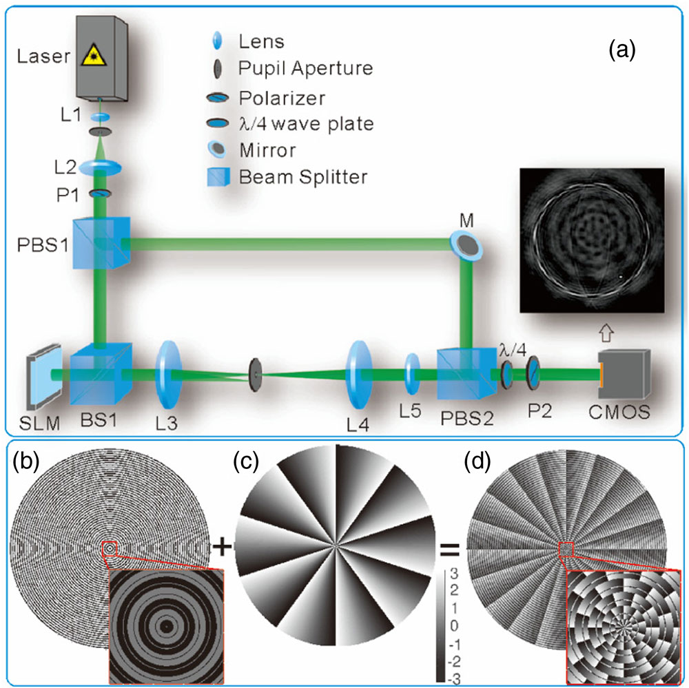
    Fig. 1. Schematic diagrams of the experimental scheme. (a) The proof-of-principle experimental setup. L12 are lenses for expanding and collimation. L3 and L4 are a confocal lens pair, and L5 is the focusing lens; PBS12 are polarizing beam splitter cubes; BS1 is a non-polarizing beam splitter; M is a reflective mirror; SLM denotes a spatial light modulator; P12 denote polarizers; λ/4 denotes a quarter-wave plate. CMOS denotes a complementary metal-oxide semiconductor camera. (b) Phase distributions of a typical binary CDG, (c) a spiral phase, and (d) the CDG embedded with the spiral phase. The insets in the bottom-right corner indicate the enlarged portions in those rectangular areas in (b) and (d), respectively.
    Simulation and experimental results of dark POVs generated by CDGs embedded with spiral phases with charges of (a) l=1, (b) −5, and (c) 15. In each box, the simulation results of the intensity distribution and interferograms are shown in the first and second rows; the experimental results of the intensity distribution and interferograms are shown in the third and fourth rows, respectively. The insets are enlarged portions of dark impulse rings in rectangular areas in those sub-images for intensity distribution. The scale bar denotes 300 μm.
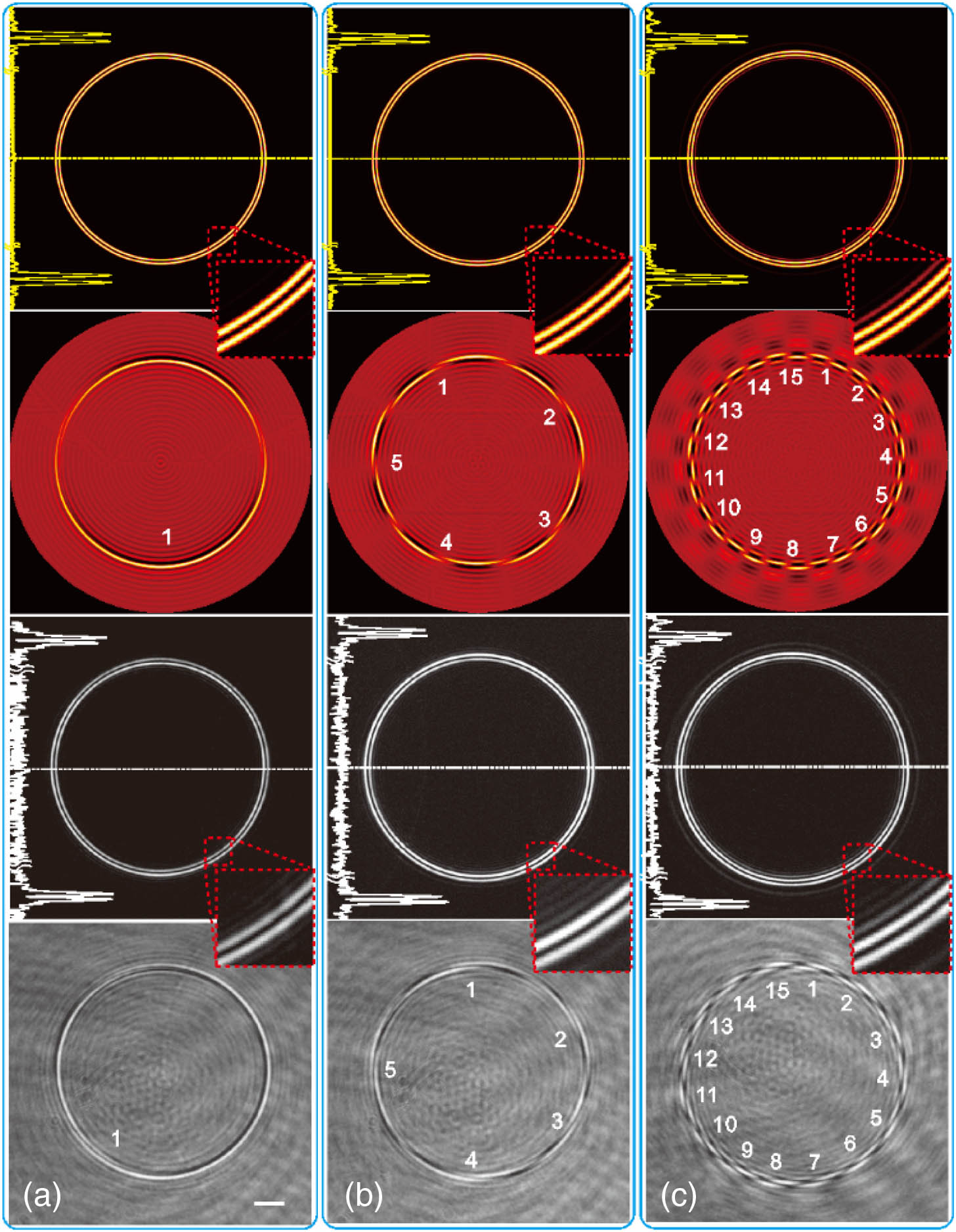
    Fig. 2. Simulation and experimental results of dark POVs generated by CDGs embedded with spiral phases with charges of (a) l=1, (b) 5, and (c) 15. In each box, the simulation results of the intensity distribution and interferograms are shown in the first and second rows; the experimental results of the intensity distribution and interferograms are shown in the third and fourth rows, respectively. The insets are enlarged portions of dark impulse rings in rectangular areas in those sub-images for intensity distribution. The scale bar denotes 300 μm.
    Simulation and experimental results of interferograms on defocused planes (with defocus distance Δd=10 mm) for dark POVs with charges of (a) l=10 and (b) −5. In each box, the simulation and experimental results are shown in the first and second rows, and the results on defocused planes before and after the focus are shown in the first and second columns, respectively. The scale bar denotes 300 μm.
    Fig. 3. Simulation and experimental results of interferograms on defocused planes (with defocus distance Δd=10  mm) for dark POVs with charges of (a) l=10 and (b) 5. In each box, the simulation and experimental results are shown in the first and second rows, and the results on defocused planes before and after the focus are shown in the first and second columns, respectively. The scale bar denotes 300 μm.
    Simulation and experimental results of phase distributions on defocused planes (with defocus distance Δd=25 mm) for dark POVs with charges of (a) l=10 and (b) l=−5. In each box, the simulation and the experimental results are shown in the first and second rows, and the results on defocused planes before and after the focus are shown in the first and second columns, respectively. The scale bar denotes 300 μm.
    Fig. 4. Simulation and experimental results of phase distributions on defocused planes (with defocus distance Δd=25  mm) for dark POVs with charges of (a) l=10 and (b) l=5. In each box, the simulation and the experimental results are shown in the first and second rows, and the results on defocused planes before and after the focus are shown in the first and second columns, respectively. The scale bar denotes 300 μm.
    Simulation and experimental results of bright POVs generated by CDGs embedded with spiral phases with charges of (a) l=1, (b) −5, and (c) 20. In each box, the simulation results of the intensity distributions and interferograms are shown in the first and second rows; the experimental results of the intensity distributions and interferograms are shown in the third and fourth rows, respectively. The insets are enlarged portions of bright impulse rings in rectangular areas in those sub-figures for intensity distribution. The scale bar denotes 300 μm.
    Fig. 5. Simulation and experimental results of bright POVs generated by CDGs embedded with spiral phases with charges of (a) l=1, (b) 5, and (c) 20. In each box, the simulation results of the intensity distributions and interferograms are shown in the first and second rows; the experimental results of the intensity distributions and interferograms are shown in the third and fourth rows, respectively. The insets are enlarged portions of bright impulse rings in rectangular areas in those sub-figures for intensity distribution. The scale bar denotes 300 μm.
    Simulation and experimental results of POVs with tunable ring profiles generated by CDGs (with period number of N=30 inside the aperture) embedded with spiral phase with charge of l=10. (a) The curve of the side-lobe ratio β as a function of the phase difference δϕ; a POV with side-lobe ratio of (b) 1/3 with a lobe ring outside, (c) 1/3 with a lobe ring inside, (d) 2/3 with a lobe ring inside, and (e) 2/3 with a lobe ring outside; (f) a POV with a bright ring profile (a bright POV with the smallest side-lobe ratio), and (g) denotes its interferogram on the focal plane; (h) a POV with a dark ring profile (a dark POV with unity side-lobe ratio), and (i) is its interferogram on the focal plane. The scale bar denotes 500 μm.
    Fig. 6. Simulation and experimental results of POVs with tunable ring profiles generated by CDGs (with period number of N=30 inside the aperture) embedded with spiral phase with charge of l=10. (a) The curve of the side-lobe ratio β as a function of the phase difference δϕ; a POV with side-lobe ratio of (b) 1/3 with a lobe ring outside, (c) 1/3 with a lobe ring inside, (d) 2/3 with a lobe ring inside, and (e) 2/3 with a lobe ring outside; (f) a POV with a bright ring profile (a bright POV with the smallest side-lobe ratio), and (g) denotes its interferogram on the focal plane; (h) a POV with a dark ring profile (a dark POV with unity side-lobe ratio), and (i) is its interferogram on the focal plane. The scale bar denotes 500 μm.
    Influences of topological charge and period number on performance parameters of POVs with bright and dark ring profiles generated by CDGs. (a) The ring radius, (b) the ring width, and (c) the side-lobe ratio as a function of the charge; (d) the ring radius, (e) the ring width, and (f) the side-lobe ratio versus the period number inside the aperture. In each sub-figure, the blue solid line denotes the simulation results of POVs with bright ring profiles (bright POVs) and the red broken line denotes the simulation results of POVs with dark ring profiles (dark POVs); the square denotes the experimental results of bright POVs, and the circle is the experimental results of dark POVs.
    Fig. 7. Influences of topological charge and period number on performance parameters of POVs with bright and dark ring profiles generated by CDGs. (a) The ring radius, (b) the ring width, and (c) the side-lobe ratio as a function of the charge; (d) the ring radius, (e) the ring width, and (f) the side-lobe ratio versus the period number inside the aperture. In each sub-figure, the blue solid line denotes the simulation results of POVs with bright ring profiles (bright POVs) and the red broken line denotes the simulation results of POVs with dark ring profiles (dark POVs); the square denotes the experimental results of bright POVs, and the circle is the experimental results of dark POVs.
    Junjie Yu, Chaofeng Miao, Jun Wu, Changhe Zhou. Circular Dammann gratings for enhanced control of the ring profile of perfect optical vortices[J]. Photonics Research, 2020, 8(5): 648
    Download Citation