Songyan Xue, Huace Hu, Yinuo Xu, Yingchen Wang, Jing Long, Binzhang Jiao, Yuncheng Liu, Xuhao Fan, Hui Gao, Leimin Deng, Wei Xiong. Research Progress and Application of Femtosecond Laser-Induced Patterned Growth of Nanomaterials[J]. Chinese Journal of Lasers, 2022, 49(12): 1202001
Search by keywords or author
- Chinese Journal of Lasers
- Vol. 49, Issue 12, 1202001 (2022)
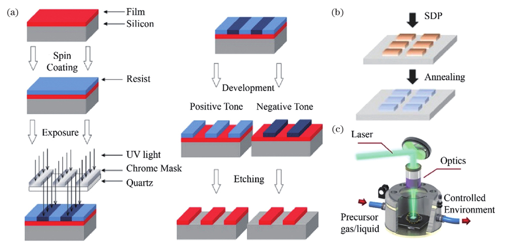
![Existing in situ synthesis methods of patterned nanomaterials[23,25-26]. (a) UV photolithography/E-beam lithography; (b) solution direct-patterning technology; (c) CW/long pulsed laser selectively induced synthesis](/richHtml/zgjg/2022/49/12/1202001/img_01.jpg)
Fig. 1. Existing in situ synthesis methods of patterned nanomaterials[23,25-26]. (a) UV photolithography/E-beam lithography; (b) solution direct-patterning technology; (c) CW/long pulsed laser selectively induced synthesis
![CW/long pulsed laser induced synthesis of metal, molybdenum sulfide, zinc oxide nanowires, and graphene[33,35-37]. (a) Cu nanoparticles synthesized by laser-induced photoreduction; (b)(c) AFM characterization results of synthesized molybdenum sulfide; (d)(e) Raman spectroscopy characterization results of synthesized molybdenum sulfide; (f) SEM image of synthesized zinc oxide nanowires; (g) TEM characterization result of synthesized zinc oxide nanowires; (h) optical micrograph of graphene synthesized by laser induced chemical vapor deposition; (i) Raman spectroscopy characterization result of graphene synthesized by laser induced chemical vapor deposition](/richHtml/zgjg/2022/49/12/1202001/img_02.jpg)
Fig. 2. CW/long pulsed laser induced synthesis of metal, molybdenum sulfide, zinc oxide nanowires, and graphene[33,35-37]. (a) Cu nanoparticles synthesized by laser-induced photoreduction; (b)(c) AFM characterization results of synthesized molybdenum sulfide; (d)(e) Raman spectroscopy characterization results of synthesized molybdenum sulfide; (f) SEM image of synthesized zinc oxide nanowires; (g) TEM characterization result of synthesized zinc oxide nanowires; (h) optical micrograph of graphene synthesized by laser induced chemical vapor deposition; (i) Raman spectroscopy characterization result of graphene synthesized by laser induced chemical vapor deposition
Fig. 3. Comparison of single-photon absorption and multi-photon absorption[51]. (a) Electron excitation processes;(b) spatial distribution of laser energy with threshold for reaction indicated by horizontal solid line
Fig. 4. Patterned metal micro-nano structures synthesized by femtosecond laser[62-66]. (a) SEM image of miniature 3D silver bridge; (b) schematic of patterned Au nanomaterials synthesized by femtosecond laser direct writing; (c) SEM image of miniature silver pillar with magnified image shown in inset; (d) SEM image of arrayed silver pyramids; (e) SEM image of four gold electrodes connected vertically by as-synthesized silver micro-nano structures
Fig. 5. Patterned SnO2 micro-nano structure synthesized by femtosecond laser[68]. (a) Chemical reaction in precursor preparation; (b) absorption spectra of precursor before and after femtosecond laser irradiation with schematic of processing shown in inset; (c) SEM image of helical product before high temperature annealing with magnified image shown in inset; (d) SEM image of helical product after high temperature annealing with magnified image shown in inset; (e) XRD characterization result of annealed product; (f) electric test result of product; (g) test result of humidity sensor
Fig. 6. Patterned TiO2/C micro-nano structure synthesized by femtosecond laser[72]. (a) Schematics of preparations of TiO2/C micro-nano structure and its pressure sensor; (b) SEM image of product with magnified image shown in inset; (c) Raman characterization results of precursors and products synthesized under different laser processing powers; (d) test results of pressure sensor; (e) principle diagrams of pressure sensor
Fig. 7. rGO-ZnO and its UV photodetector synthesized by femtosecond laser[73]. (a) Schematics of interdigitated electrode and active detection layer prepared by changing laser scanning speed and schematics of rGO-ZnO hybrid-based photodetector prepared by single-step FLDW process; (b) EDX characterization results of products
Fig. 8. SnO2 and its photo and gas detector synthesized by femtosecond laser[69]. (a) SEM image of line pattern; (b) SEM image of“HUST”pattern; (c) magnified image of dotted box area in Fig. 8(b); (d) optical micrograph of photo and gas detector; (e) detecting result of gas detector to H2S; (f) detecting result of photo detector
Fig. 9. ZnO and its UV photodetector synthesized by femtosecond laser[70]. (a) SEM image of linear product; (b) SEM image of“HUST”pattern; (c) magnified image of dotted box area in Fig. 9(b); (d) optical micrograph of UV photodetector; (e) current-voltage test result of UV photodetector; (f) time response test result of UV photodetector
Fig. 10. Patterned molybdenum sulfide nanomaterials synthesized by femtosecond laser [75]. (a) SEM image of product; (b) SEM image of patterned product; (c) AFM characterization result of product; (d) Raman test result of product; (e) optical micrograph of product; (f) Raman mapping of product
Fig. 11. Molybdenum sulfide micro-nano gas detector prepared by femtosecond laser[75]. (a) Optical micrograph of detector; (b) response of sensor to NO2 at room temperature; (c) response of sensor to NO2 with volume fraction of 0.5×10⁻⁶ at room temperature; (d) time response of sensor at 50 ℃;(e) response of sensor to H2S at room temperature; (f) response of sensor to NH3 at room temperature
Fig. 12. Patterned graphene nanomaterials synthesized by femtosecond laser[85,89]. (a) Processing schematic of femtosecond laser-induced patterned graphene on Ni/C thin films; (b) processing schematic of femtosecond laser-induced reduction of graphene oxide; (c) optical micrograph of patterned graphene product; (d) Raman mapping characterization of patterned graphene product; (e) optical micrograph of graphene spiral microcircuit structure; (f) optical micrograph of graphene comb-like microcircuit
Fig. 13. Laser-induced preparation of patterned graphene nanomaterials and graphene-based super-capacitors[91-92]. (a) Processing schematic of CW laser-induced preparation of graphene-based super-capacitor and its SEM images; (b) processing schematic of femtosecond laser-induced preparation of graphene-based super-capacitors; (c)-(g) optical micrographs of graphene-based super-capacitors prepared by femtosecond laser
|
Table 1. Summary of selectively induced synthesis of nanomaterials by CW/long pulsed laser[32-36,38,40-41]
|

Set citation alerts for the article
Please enter your email address


