Nanomaterials with small features and large surface-to-volume ratios have drawn tremendous research attention in various fields including energy devices, microelectronics, and biomedicine. By far, researchers have realized high-quality fabrication of various nanomaterials through solid-phase, liquid-phase, or vapor-phase method. However, the fabrication of nanomaterial-based functional devices usually requires subsequent material transfer and assembly processes. Therefore, to effectively realize the integration of nanomaterials and make full use of their unique properties, the transfer-free growth of patterned nanomaterials is very important.
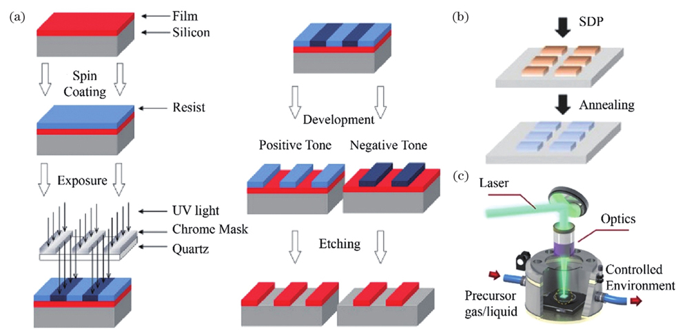
Although methods have been developed to realize the in-situ transfer-free patterned growth of nanomaterials, such as ultraviolet lithography, electron beam lithography, solution-based direct-patterning technique, and continuous wave/long pulsed laser selective induction, it is still difficult to meet the demands of customized patterning, precise processing, and in-situ heterogeneous integration of nanomaterials on thermal-sensitive, flexible, and curved substrates. The UV lithography and electron beam lithography techniques are cumbersome, time-consuming, and usually need a vacuum chamber. Besides, they are difficult to apply to curved substrates. The solution-based direct-patterning technique requires the subsequent high-temperature annealing process, which is difficult to apply to thermal sensitive substrates. The CW/long pulsed laser selective induction method is difficult to achieve high precision and highly localized growth due to the diffraction limit effect and the sizeable heat-affected zone.
Due to these drawbacks of the existing methods, researchers have attempted to use a femtosecond laser to realize the direct patterned growth of nanomaterials. As a "cold processing" method with a high peak power, the femtosecond laser direct writing is a promising tool to achieve the direct patterned growth of nanomaterials. The focus of a femtosecond laser can be regarded as a flexible, controllable and highly localized micro-reactor, which can realize the fixed-point growth of nanomaterials. At the same time, according to the pre-designed patterns, the laser focus position can be changed by the galvanometer, displacement stage or other equipment to realize the transfer-free patterned growth of nanomaterials. Compared with the current commonly used CW or long pulsed laser, a femtosecond laser has unique advantages in the transfer-free patterned growth of nanomaterials. First, due to its small heat-affected zone, it can be applied to thermal-sensitive substrates. Second, the ultra-high energy density of a femtosecond laser can induce nonlinear multi-photon absorption of precursors, which can realize the direct absorption of laser energy. Therefore, the femtosecond laser induced direct patterned growth of nanomaterials can be applied to transparent substrates without heat-absorbing layers. Third, the threshold effect of nonlinear absorption and the small heat-affected zone of a femtosecond laser can realize the high-precision growth of nanomaterials. Thus, the femtosecond laser induced patterned growth of nanomaterials has unique advantages and excellent prospects.
In this review, we first summarize the commonly used patterned synthesis methods of nanomaterials and their problems, including UV/electron beam lithography, solution-based direct patterning, and CW/long pulsed laser induced growth of nanomaterials. Then we discuss the unique advantages of the femtosecond laser-induced patterned growth method of nanomaterials, including high precision, highly localized growth, and high processing compatibility with thermal sensitive and transparent substrates. Next, the recent progress of the femtosecond laser induced direct patterned growth of nanomaterials and their applications are reviewed, including metal, metal oxide, metal sulfide, and carbon-based nanomaterials. For metal materials, researchers realized silver and gold patterned micro-nano structures with high conductivity [Fig.4(a)], which are comparable to the bulk materials. To grow more high-precision products, researchers realized silver nanostructures with a minimum feature size of only 180 nm with the help of surfactant [Fig.4(c)]. Researchers realized a stable 3D connection between two pairs of metal electrodes. As for metal oxides, researchers realized the patterned SnO2structure with the line width of about 150 nm through femtosecond laser direct writing (FLDW) and subsequent annealing process (Fig. 5). Our group realized the patterned growth of ZnO and SnO2 through femtosecond laser direct writing without subsequent annealing (Figs. 8 and 9). The minimum linewidth is about 800 nm. For metal sulfide, our group realized the patterned growth of MoS2 through femtosecond laser induced photochemical reaction (Fig. 10). For carbon-based nanomaterials, researchers realized the patterned growth of graphene through femtosecond laser induced reduction of graphene oxide [Fig.12(b)]. Researchers realized the patterned growth of graphene through FLDW of co-sputtering Ni/C films. The sheet resistivity of the products is about 205 Ω/sq [Fig.12(a)].
Compared with traditional methods, the femtosecond laser induced direct patterned growth technique has many unique advantages. Due to the extremely small heat-affected zone and the nonlinear multi-photon absorption effect of a femtosecond laser, the femtosecond laser induced direct patterned growth technique can realize the high precision, highly localized patterned growth of nanomaterials and has high processing compatibility with thermal sensitive and transparent substrates. Besides, the femtosecond laser induced direct patterned growth technique does not need a vacuum chamber or the high-temperature annealing process. Thus, it has drawn tremendous research attention around the world. Although the femtosecond laser induced direct patterned growth technique has made some progresses, several problems remain to be resolved. First, the products need to be expanded and the precursor needs to be optimized to reduce the required laser energy and take full use of the advantages of a femtosecond laser. Second, in term of the processing system, a Gaussian beam can be converted into a flat-top beam by beam shaping, thereby improving the uniformity of the products. The processing efficiency can be improved by employing scanning devices with high scanning frequency or adopting parallel processing strategies including multi-point scanning, line scanning , and plane projection. Finally, the application of this method needs to be explored, such as MEMS, soft electronics, metasurfaces, energy and catalytic devices.