• Advanced Photonics
  • Vol. 2, Issue 1, 014002 (2020)
Yang Yu1、†, Ting-Hui Xiao2、*, Yunzhao Wu2, Wanjun Li1, Qing-Guang Zeng1, Li Long3, and Zhi-Yuan Li3、*
Author Affiliations
  • 1Wuyi University, School of Applied Physics and Materials, Jiangmen, China
  • 2University of Tokyo, Department of Chemistry, Tokyo, Japan
  • 3South China University of Technology, School of Physics and Optoelectronics, Guangzhou, China
  • show less
    DOI: 10.1117/1.AP.2.1.014002 Cite this Article Set citation alerts
    Yang Yu, Ting-Hui Xiao, Yunzhao Wu, Wanjun Li, Qing-Guang Zeng, Li Long, Zhi-Yuan Li. Roadmap for single-molecule surface-enhanced Raman spectroscopy[J]. Advanced Photonics, 2020, 2(1): 014002 Copy Citation Text show less
    Plasmonic nanogaps with precise size control for single-molecule SERS. (a) Scanning electron microscope image of an optical antenna. Inner and outer radii of silver rings are 300 and 380 nm, respectively. Left-hand rod is 80 nm long and 70 nm wide. Right-hand rod is 68 nm long and 62 nm wide. (b) Representative Raman spectra of R6G-d0 and R6G-d4 single-molecule level events. The R6G-d4 spectrum is shifted in the vertical direction by 2000 counts for display purposes.47" target="_self" style="display: inline;">47 (c) Nanometer-scale silver-shell growth-based gap-engineering in the formation of the SERS-active GSND. (d) Raman spectra taken from Cy3-modified oligonucleotides (redline) and Cy3-free oligonucleotides (blackline) in NaCl-aggregated silver colloids.69" target="_self" style="display: inline;">69 (e) Schematic of the NP dimers assembled on the DNA origami platform. The NPs are coated with an ssDNA brush to prevent aggregation as well as facilitate attachment to the origami platform. (f) Measured Raman spectra of the ssDNA coating of 19 bases of thymine (sequence 1) on the NP dimers.70" target="_self" style="display: inline;">70 (g) SECARS enhancement map. (h) Three representative SECARS spectra showing a pure p-MA event (top), a pure adenine event (middle), and a mixed event (bottom).48" target="_self" style="display: inline;">48 Figures reprinted with permission: (a) and (b) Ref. 47, © 2013 by the American Chemical Society; (c) and (d) Ref. 69, © 2009 by the Nature Publishing Group; (e) and (f) Ref. 70, © 2014 by the Nature Publishing Group; and (g) and (h) Ref. 48, © 2014 by the Nature Publishing Group.
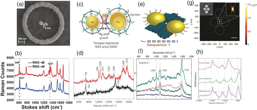
    Fig. 1. Plasmonic nanogaps with precise size control for single-molecule SERS. (a) Scanning electron microscope image of an optical antenna. Inner and outer radii of silver rings are 300 and 380 nm, respectively. Left-hand rod is 80 nm long and 70 nm wide. Right-hand rod is 68 nm long and 62 nm wide. (b) Representative Raman spectra of R6G-d0 and R6G-d4 single-molecule level events. The R6G-d4 spectrum is shifted in the vertical direction by 2000 counts for display purposes.47 (c) Nanometer-scale silver-shell growth-based gap-engineering in the formation of the SERS-active GSND. (d) Raman spectra taken from Cy3-modified oligonucleotides (redline) and Cy3-free oligonucleotides (blackline) in NaCl-aggregated silver colloids.69 (e) Schematic of the NP dimers assembled on the DNA origami platform. The NPs are coated with an ssDNA brush to prevent aggregation as well as facilitate attachment to the origami platform. (f) Measured Raman spectra of the ssDNA coating of 19 bases of thymine (sequence 1) on the NP dimers.70 (g) SECARS enhancement map. (h) Three representative SECARS spectra showing a pure p-MA event (top), a pure adenine event (middle), and a mixed event (bottom).48 Figures reprinted with permission: (a) and (b) Ref. 47, © 2013 by the American Chemical Society; (c) and (d) Ref. 69, © 2009 by the Nature Publishing Group; (e) and (f) Ref. 70, © 2014 by the Nature Publishing Group; and (g) and (h) Ref. 48, © 2014 by the Nature Publishing Group.
    Plasmonic sharp tips for single-molecule SERS. (a) An illustration of the FM-TERS system for simultaneous conductance and TERS measurement of single-molecule junctions. A gold (111) surface is preadsorbed with molecules. The distance between the gold tip and the gold (111) surface is then controlled by an STM equipped with a conductance-measuring circuit. The red contour indicates the distribution of electromagnetic field strength between the tip and the substrate. Wavy arrows indicate Raman scattering by the molecules. (b) The Raman band of 4bipy (1609 cm−1) is seen to change with the bias voltage. Inset: current versus bias curve for 4bipy obtained with a mechanical break-junction setup.72" target="_self" style="display: inline;">72 (c) Schematic of tunneling-controlled TERS in a confocal-type side-illumination configuration, in which Vb is the sample bias and It is the tunneling current. (d) The top panels show experimental TERS mapping of a single molecule for different Raman peaks (23×23, ∼0.16 nm per pixel), processed from all individual TERS spectra acquired at each pixel (120 mV, 1 nA, 0.3 s; image size: 3.6×3.6 nm2). The middle panels show the theoretical simulation of the TERS mapping. The left bottom panel shows a height profile of a line trace in the inset STM topograph (1 V, 20 pA). The right bottom panel shows a TERS intensity profile of the same line trace for the inset Raman map associated with the 817 cm−1 Raman peak.73" target="_self" style="display: inline;">73 (e) The hollow conical taper and the taper with spiral corrugations along the conical surface (top panel). The simulated E-field intensity distributions in the x-z plane for the two structures with x-polarized incident light at the wavelength of 800 nm (bottom panel). (f) The side-view SEM image of fabricated spiral taper (left panel) and the false-color image of focus pattern of gold-coated spiral taper under linearly polarized excitation with x-direction polarization (right panel).74" target="_self" style="display: inline;">74 Figures reprinted with permission: (a) and (b) Ref. 72, © 2011 by the Nature Publishing Group; (c) and (d) Ref. 73, © 2013 by the Nature Publishing Group; and (e) and (f) Ref. 74, © 2014 by Wiley-VCH Verlag.
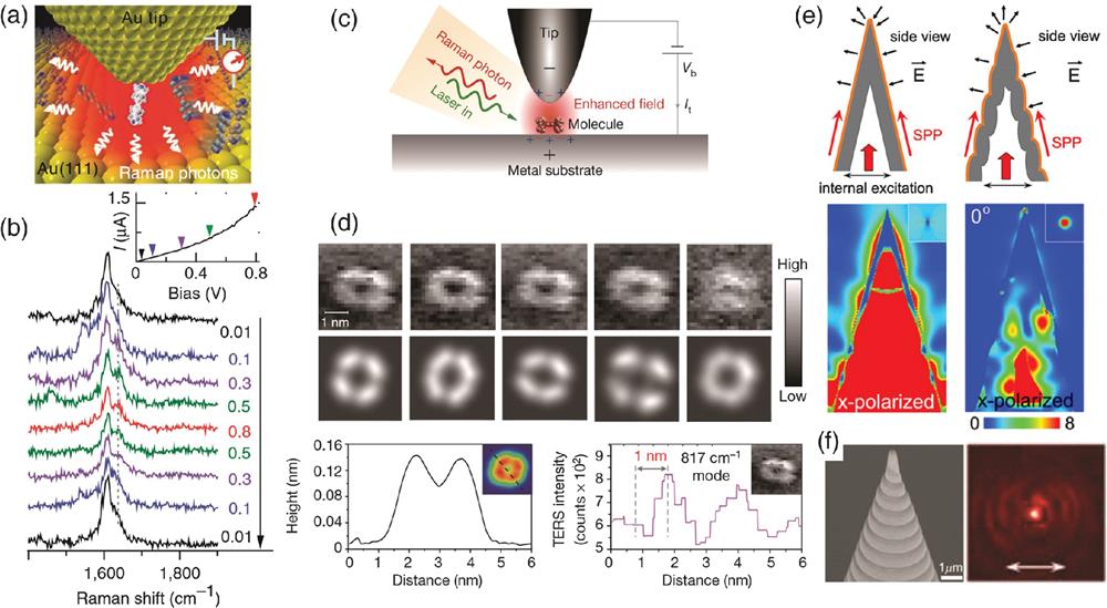
    Fig. 2. Plasmonic sharp tips for single-molecule SERS. (a) An illustration of the FM-TERS system for simultaneous conductance and TERS measurement of single-molecule junctions. A gold (111) surface is preadsorbed with molecules. The distance between the gold tip and the gold (111) surface is then controlled by an STM equipped with a conductance-measuring circuit. The red contour indicates the distribution of electromagnetic field strength between the tip and the substrate. Wavy arrows indicate Raman scattering by the molecules. (b) The Raman band of 4bipy (1609  cm1) is seen to change with the bias voltage. Inset: current versus bias curve for 4bipy obtained with a mechanical break-junction setup.72 (c) Schematic of tunneling-controlled TERS in a confocal-type side-illumination configuration, in which Vb is the sample bias and It is the tunneling current. (d) The top panels show experimental TERS mapping of a single molecule for different Raman peaks (23×23, 0.16  nm per pixel), processed from all individual TERS spectra acquired at each pixel (120 mV, 1 nA, 0.3 s; image size: 3.6×3.6nm2). The middle panels show the theoretical simulation of the TERS mapping. The left bottom panel shows a height profile of a line trace in the inset STM topograph (1 V, 20 pA). The right bottom panel shows a TERS intensity profile of the same line trace for the inset Raman map associated with the 817  cm1 Raman peak.73 (e) The hollow conical taper and the taper with spiral corrugations along the conical surface (top panel). The simulated E-field intensity distributions in the x-z plane for the two structures with x-polarized incident light at the wavelength of 800 nm (bottom panel). (f) The side-view SEM image of fabricated spiral taper (left panel) and the false-color image of focus pattern of gold-coated spiral taper under linearly polarized excitation with x-direction polarization (right panel).74 Figures reprinted with permission: (a) and (b) Ref. 72, © 2011 by the Nature Publishing Group; (c) and (d) Ref. 73, © 2013 by the Nature Publishing Group; and (e) and (f) Ref. 74, © 2014 by Wiley-VCH Verlag.
    Plasmonic complex nanostructures for single-molecule SERS. (a) Concept of a complex SERS substrate with the function of electrostatic precipitation for effective localized collection and identification of molecules. The inset is the scanning electron microscope image of the SERS substrate. (b) Raman intensity on the biased substrates is increased by a factor of 615.76" target="_self" style="display: inline;">76 (c) Schematic diagram of the setup for nanoslit SERS. The nanoslit chip is sealed in a flow cell, which separates the electrolyte solution into two compartments. The top chamber can accommodate a water-immersion objective lens. A 785-nm laser with 8 mW is focused on the gold nanoslit. Axon patch 200B amplifier is used to apply the transmembrane voltages and monitor the ionic currents between two Ag/AgCl electrodes. The inset shows a top-view SEM image of the nanoslit structure, consisting of an inverted prism nanoslit cavity with Bragg-mirror gratings. The scale bar is 1 μm. (d) The contour maps of SERS of a typical asynchronous blinking of the mixed isotopic adenines (top panel) and a typical fluctuation of the single adenine (bottom) recorded in 5 s, respectively, in single-molecule sensing.77" target="_self" style="display: inline;">77 (e) 3-D finite-difference time-domain simulations for a Ag nanoparticle on a warped Au substrate. A prominent field enhancement is demonstrated due to the effective gradient of permittivity. The right panel shows the SEM image of the substrate where the scale bar is 500 nm. (f) Typical spectra for bianalyte analysis.78" target="_self" style="display: inline;">78 Figures reprinted with permission: (a) and (b) Ref. 76, © 2013 by the Nature Publishing Group; (c) and (d) Ref. 77, © 2018 by the Nature Publishing Group; and (e) and (f) Ref. 78, © 2018 by the Nature Publishing Group.
    Fig. 3. Plasmonic complex nanostructures for single-molecule SERS. (a) Concept of a complex SERS substrate with the function of electrostatic precipitation for effective localized collection and identification of molecules. The inset is the scanning electron microscope image of the SERS substrate. (b) Raman intensity on the biased substrates is increased by a factor of 615.76 (c) Schematic diagram of the setup for nanoslit SERS. The nanoslit chip is sealed in a flow cell, which separates the electrolyte solution into two compartments. The top chamber can accommodate a water-immersion objective lens. A 785-nm laser with 8 mW is focused on the gold nanoslit. Axon patch 200B amplifier is used to apply the transmembrane voltages and monitor the ionic currents between two Ag/AgCl electrodes. The inset shows a top-view SEM image of the nanoslit structure, consisting of an inverted prism nanoslit cavity with Bragg-mirror gratings. The scale bar is 1  μm. (d) The contour maps of SERS of a typical asynchronous blinking of the mixed isotopic adenines (top panel) and a typical fluctuation of the single adenine (bottom) recorded in 5 s, respectively, in single-molecule sensing.77 (e) 3-D finite-difference time-domain simulations for a Ag nanoparticle on a warped Au substrate. A prominent field enhancement is demonstrated due to the effective gradient of permittivity. The right panel shows the SEM image of the substrate where the scale bar is 500 nm. (f) Typical spectra for bianalyte analysis.78 Figures reprinted with permission: (a) and (b) Ref. 76, © 2013 by the Nature Publishing Group; (c) and (d) Ref. 77, © 2018 by the Nature Publishing Group; and (e) and (f) Ref. 78, © 2018 by the Nature Publishing Group.
    Chemical enhancement for single-molecule SERS. (a) A typical energy diagram of a substrate–molecule hybrid system consisting of a metal SERS substrate and an adsorbed molecule.80" target="_self" style="display: inline;">80 (b) Scanning electron microscopy image for W18O49 sample. Inset in (b): high-resolution transmission electron microscopy image on one single nanowire illustrating clear lattice fringe of 0.38 nm, which suggested that the nanowire growth was along the [010] direction. (c) Improved SERS properties of W18O49 samples after Ar/H2 annealing treatment. Raman signals of R6G molecule on pristine W18O49 and the samples after annealing treatment (in Ar/H2 for 1 h). The tested concentration of R6G was 1×10⁻⁶ M. (d) A comparison of Raman EF for the two respective vibration modes P1 and P3. Data reported in this histogram resulted from Raman spectra acquired over 30 different regions per sample and provide an indication of the EF for each Raman mode. The H2-treated sample shows the greatest enhancement at band P1, the EF for which was evaluated to be 3.4×105.8" target="_self" style="display: inline;">8 (e) Raman spectra collected for oxygen-incorporated MoS2 sample annealed for 40 min at four different concentrations, 10−4, 10−5, 10−6, and 10−7 M, suggesting the detection limit was as low as 10−7 M. (f) SERS spectra on the oxygen-incorporated MoS2 samples with different annealing temperatures. (g) and (h) SERS spectra of R6G on a series of other semiconductor materials WS2 and MoSe2 respectively.23" target="_self" style="display: inline;">23 Figures reprinted with permission: (a) and (b) Ref. 80, © 1986 by the American Institute of Physics; (c) and (d) Ref. 8, © 2015 by the Nature Publishing Group; (e)–(h) Ref. 23, © 2015 by the Nature Publishing Group.
    Fig. 4. Chemical enhancement for single-molecule SERS. (a) A typical energy diagram of a substrate–molecule hybrid system consisting of a metal SERS substrate and an adsorbed molecule.80 (b) Scanning electron microscopy image for W18O49 sample. Inset in (b): high-resolution transmission electron microscopy image on one single nanowire illustrating clear lattice fringe of 0.38 nm, which suggested that the nanowire growth was along the [010] direction. (c) Improved SERS properties of W18O49 samples after Ar/H2 annealing treatment. Raman signals of R6G molecule on pristine W18O49 and the samples after annealing treatment (in Ar/H2 for 1 h). The tested concentration of R6G was 1×10⁶  M. (d) A comparison of Raman EF for the two respective vibration modes P1 and P3. Data reported in this histogram resulted from Raman spectra acquired over 30 different regions per sample and provide an indication of the EF for each Raman mode. The H2-treated sample shows the greatest enhancement at band P1, the EF for which was evaluated to be 3.4×105.8 (e) Raman spectra collected for oxygen-incorporated MoS2 sample annealed for 40 min at four different concentrations, 104, 105, 106, and 107  M, suggesting the detection limit was as low as 107  M. (f) SERS spectra on the oxygen-incorporated MoS2 samples with different annealing temperatures. (g) and (h) SERS spectra of R6G on a series of other semiconductor materials WS2 and MoSe2 respectively.23 Figures reprinted with permission: (a) and (b) Ref. 80, © 1986 by the American Institute of Physics; (c) and (d) Ref. 8, © 2015 by the Nature Publishing Group; (e)–(h) Ref. 23, © 2015 by the Nature Publishing Group.
    Potential strategy for single-molecule SERS enabled by Rayleigh scattering-assisted Raman enhancement theory. Schematic configuration of TERS system used for Raman mapping of molecule (a) with and (b) without molecule selfinteraction. (c) The excitation process in classical Raman physics, where the incident light is scattered by the Ag tip–substrate nanogap to form highly localized plasmonic gap mode with greatly enhanced electric field intensity. E0 and Es (yellow arrows) are the incident and scattering electric fields, summing up to the local field E. (d) The radiation process in classical Raman physics, where the Raman signal emitted by the molecule is scattered by the Ag–substrate gap to have greatly enhanced far-field intensity. G0·μ and Gs·μ (blue arrows) are the direct Raman radiation of molecule (described by the dipole moment μ) and greatly enhanced scattering Raman radiation by the tip–substrate nanogap, where G0 and Gs are free-space and scattering dyadic Green’s function. (e) The excitation process in the extended Raman physics considering the molecule selfinteraction with the Ag tip–substrate gap through multiple elastic scattering (white arrows, abbreviated by E.S.) for the incident light. Em,s is the modified excitation field due to the E.S. mechanism and p is the induced dipole moment. (f) The radiation process in the extended Raman physics when considering the molecule selfinteraction. The multiple E.S. mechanism (white arrows) strongly modifies the molecule dipole moment to a value μN,R.90" target="_self" style="display: inline;">90 (a)–(f) Figures reprinted with permission from Ref. 90, © 1986 by the American Chemical Society.
    Fig. 5. Potential strategy for single-molecule SERS enabled by Rayleigh scattering-assisted Raman enhancement theory. Schematic configuration of TERS system used for Raman mapping of molecule (a) with and (b) without molecule selfinteraction. (c) The excitation process in classical Raman physics, where the incident light is scattered by the Ag tip–substrate nanogap to form highly localized plasmonic gap mode with greatly enhanced electric field intensity. E0 and Es (yellow arrows) are the incident and scattering electric fields, summing up to the local field E. (d) The radiation process in classical Raman physics, where the Raman signal emitted by the molecule is scattered by the Ag–substrate gap to have greatly enhanced far-field intensity. G0·μ and Gs·μ (blue arrows) are the direct Raman radiation of molecule (described by the dipole moment μ) and greatly enhanced scattering Raman radiation by the tip–substrate nanogap, where G0 and Gs are free-space and scattering dyadic Green’s function. (e) The excitation process in the extended Raman physics considering the molecule selfinteraction with the Ag tip–substrate gap through multiple elastic scattering (white arrows, abbreviated by E.S.) for the incident light. Em,s is the modified excitation field due to the E.S. mechanism and p is the induced dipole moment. (f) The radiation process in the extended Raman physics when considering the molecule selfinteraction. The multiple E.S. mechanism (white arrows) strongly modifies the molecule dipole moment to a value μN,R.90 (a)–(f) Figures reprinted with permission from  Ref. 90, © 1986 by the American Chemical Society.
    Process monitoring of chemical catalysis by single-molecule SERS. (a) SERS spectra of 10−7 MpNTP excited at 3, 15, and 30 mW laser power, respectively. (b) SERS spectra of 10−8 MpNTP excited at 0.015, 0.15, and 1.5 mW laser power, respectively. (c) From top to bottom: Time-dependent SERS spectra of reacting pNTP (c=10−9 M) at 3 mW laser at 2, 6, and 30 min; normal SERS spectra of TP and pNTP, respectively.29" target="_self" style="display: inline;">29 (d) Selfassembled 80-nm nanoparticle-on-mirror geometry used to elicit field enhancements required for single-molecule spectroscopy. (e) Short (0.9 s) segment from NPoM time scan showing the reduction and oxidation processes.30" target="_self" style="display: inline;">30 (f) Schematic diagram showing the configuration of an L-GNP/S-GNP dimer linked with 1,6-hexanedithiol. (g) (top) Schematic illustration showing the S-GNP catalyzed reduction of 4-NTP in the presence of borohydride. (bottom) Color-coded intensity map of time-dependent single-NP SERS spectra after borohydride addition, with a range of Raman shifts between 900 and 1800 cm−1 for a 1 s integration time, taken every 5 s at 638 nm.31" target="_self" style="display: inline;">31 Figures reprinted with permission: (a)–(c) Ref. 29, © 2015 by the Royal Society of Chemistry; (d) and (e) Ref. 30, © 2017 by the Nature Publishing Group; and (f) and (g) Ref. 31, © 2019 by the Royal Society of Chemistry.
    Fig. 6. Process monitoring of chemical catalysis by single-molecule SERS. (a) SERS spectra of 107  MpNTP excited at 3, 15, and 30 mW laser power, respectively. (b) SERS spectra of 108  MpNTP excited at 0.015, 0.15, and 1.5 mW laser power, respectively. (c) From top to bottom: Time-dependent SERS spectra of reacting pNTP (c=109  M) at 3 mW laser at 2, 6, and 30 min; normal SERS spectra of TP and pNTP, respectively.29 (d) Selfassembled 80-nm nanoparticle-on-mirror geometry used to elicit field enhancements required for single-molecule spectroscopy. (e) Short (0.9 s) segment from NPoM time scan showing the reduction and oxidation processes.30 (f) Schematic diagram showing the configuration of an L-GNP/S-GNP dimer linked with 1,6-hexanedithiol. (g) (top) Schematic illustration showing the S-GNP catalyzed reduction of 4-NTP in the presence of borohydride. (bottom) Color-coded intensity map of time-dependent single-NP SERS spectra after borohydride addition, with a range of Raman shifts between 900 and 1800  cm1 for a 1 s integration time, taken every 5 s at 638 nm.31 Figures reprinted with permission: (a)–(c) Ref. 29, © 2015 by the Royal Society of Chemistry; (d) and (e) Ref. 30, © 2017 by the Nature Publishing Group; and (f) and (g) Ref. 31, © 2019 by the Royal Society of Chemistry.
    Imaging of vibrational modes by single-molecule SERS. (a) Schematic of STM-controlled TERS in a confocal-type side-illumination configuration on Ag (111) using Ag tips. (b) TERS spectra acquired above ZnTPP or H2TBPP molecular islands (0.1 V, 1 nA, 30 s). For comparison, powder Raman spectra and Raman spectra calculated via DFT are also shown. The brown spectrum was taken on bare Ag (111) (0.1 V, 1 nA, 30 s) and the black spectrum was measured on top of a molecular island but with the tip retracted 5 nm from the surface (0.1 V, 30 s).32" target="_self" style="display: inline;">32 (c), (d) TERS images reconstructed based on single-peak analysis for the Raman peaks at ∼701 cm−1 (c, integrated over 687 to 736 cm−1) and ∼918 cm−1 (d, integrated over 890 to 959 cm−1). (e) STM image of two adjacent porphyrin molecular domains (−1 V, 5 pA). (f) STM image simultaneously acquired during TERS imaging of the area denoted by the dashed square in (e) (–0.1 V, 1 nA, 7 nm×7 nm, 32×32 pixels, 1 s per pixel). The boundary between the molecular domains is highlighted by a yellow line. (g) TERS spectra, averaged over the blue and green squares (3×3 pixels) shown in (f), extracted from the datacube for ZnTPP and H2TBPP molecules, respectively.33" target="_self" style="display: inline;">33 (h) Diagram of the system to detect the distribution of the electrostatic fields of single molecules. (i) Electrostatic field surface obtained by color-coding the Stark on the STM CH topography. The common image size is 23 ⏧×23 ⏧. The set point is 0.1 nA, 1.2 V. (j) Electrostatic field mapped on the isosurface of local density of states. The common image size is 27 ⏧×27 ⏧. The set point is 0.1 nA, 1.2 V.34" target="_self" style="display: inline;">34 Figures reprinted with permission: (a) and (b) Ref. 32, © 2015 by the Nature Publishing Group; (c)–(g) Ref. 33, © 2017 by the Nature Publishing Group; (h)–(j) Ref. 34, © 2018 by the American Association for the Advancement of Science.
    Fig. 7. Imaging of vibrational modes by single-molecule SERS. (a) Schematic of STM-controlled TERS in a confocal-type side-illumination configuration on Ag (111) using Ag tips. (b) TERS spectra acquired above ZnTPP or H2TBPP molecular islands (0.1 V, 1 nA, 30 s). For comparison, powder Raman spectra and Raman spectra calculated via DFT are also shown. The brown spectrum was taken on bare Ag (111) (0.1 V, 1 nA, 30 s) and the black spectrum was measured on top of a molecular island but with the tip retracted 5 nm from the surface (0.1 V, 30 s).32 (c), (d) TERS images reconstructed based on single-peak analysis for the Raman peaks at 701  cm1 (c, integrated over 687 to 736  cm1) and 918  cm1 (d, integrated over 890 to 959  cm1). (e) STM image of two adjacent porphyrin molecular domains (1  V, 5 pA). (f) STM image simultaneously acquired during TERS imaging of the area denoted by the dashed square in (e) (–0.1 V, 1 nA, 7 nm×7 nm, 32×32  pixels, 1 s per pixel). The boundary between the molecular domains is highlighted by a yellow line. (g) TERS spectra, averaged over the blue and green squares (3×3  pixels) shown in (f), extracted from the datacube for ZnTPP and H2TBPP molecules, respectively.33 (h) Diagram of the system to detect the distribution of the electrostatic fields of single molecules. (i) Electrostatic field surface obtained by color-coding the Stark on the STM CH topography. The common image size is 23  ×23  . The set point is 0.1 nA, 1.2 V. (j) Electrostatic field mapped on the isosurface of local density of states. The common image size is 27×27. The set point is 0.1 nA, 1.2 V.34 Figures reprinted with permission: (a) and (b) Ref. 32, © 2015 by the Nature Publishing Group; (c)–(g) Ref. 33, © 2017 by the Nature Publishing Group; (h)–(j) Ref. 34, © 2018 by the American Association for the Advancement of Science.
    Observation of charge transfer in nanoelectronics by single-molecule SERS. (a) Raman analysis of C60 in an electromigrated junction. (Main plot) Example of a SERS spectrum of C60 in an electromigrated junction. Surrounding diagrams illustrate examples of the complicated displacements associated with Raman-active modes, calculated for an isolated, symmetric, gas-phase molecule. Each such mode is fivefold degenerate in the absence of symmetry breaking. (Inset) Scanning electron microscopic image of an electromigrated junction. (b) Raman response of device 3 as a function of bias (x axis) and Raman shift (y axis). The sudden change in the intensity at around 0.1 V is the result of blinking. (c) Vibrational energy shift as a function of bias for three particular modes: 1258 and 1592 cm−1. The discretized Raman shift data result from pixilation of the detector.35" target="_self" style="display: inline;">35 (d), (e) SERS spectra of 4-MBA in the different TiO2–MBA–Au NR assemblies at excitation wavelengths of (d) 633 nm and (e) 785 nm. The numbers on the left side in each figure indicate the SP absorption peaks of the TiO2–MBA–Au NR assemblies. (f) Main physical mechanisms involved in plasmon-assisted charge transfer.36" target="_self" style="display: inline;">36 Figures reprinted with permission: (a)–(c) Ref. 35, © 2014 by the National Academy of Sciences; (d)–(f) Ref. 36, © 2018 by the Royal Society of Chemistry.
    Fig. 8. Observation of charge transfer in nanoelectronics by single-molecule SERS. (a) Raman analysis of C60 in an electromigrated junction. (Main plot) Example of a SERS spectrum of C60 in an electromigrated junction. Surrounding diagrams illustrate examples of the complicated displacements associated with Raman-active modes, calculated for an isolated, symmetric, gas-phase molecule. Each such mode is fivefold degenerate in the absence of symmetry breaking. (Inset) Scanning electron microscopic image of an electromigrated junction. (b) Raman response of device 3 as a function of bias (x axis) and Raman shift (y axis). The sudden change in the intensity at around 0.1 V is the result of blinking. (c) Vibrational energy shift as a function of bias for three particular modes: 1258 and 1592  cm1. The discretized Raman shift data result from pixilation of the detector.35 (d), (e) SERS spectra of 4-MBA in the different TiO2–MBA–Au NR assemblies at excitation wavelengths of (d) 633 nm and (e) 785 nm. The numbers on the left side in each figure indicate the SP absorption peaks of the TiO2–MBA–Au NR assemblies. (f) Main physical mechanisms involved in plasmon-assisted charge transfer.36 Figures reprinted with permission: (a)–(c) Ref. 35, © 2014 by the National Academy of Sciences; (d)–(f) Ref. 36, © 2018 by the Royal Society of Chemistry.
    Combination of single-molecule SERS with other techniques. (a) Ag colloids premixed with a suitable combination of bianalyte SERS partners (RH6G and NB at 2- to 5-nM concentration) are deposited on a working electrode (Ag) in an open-frame electrochemical cell (with a wide-area Pt counter electrode and a Ag/AgCl reference electrode). (b) Many molecule and SM-SERS intensity cases for NB. The varied durations of the signals in the “on” (oxidized) state reveal the different redox potentials for that particular molecule. (c) Variations in redox properties for two consecutive cycles, as determined from the SERS intensity of the 590 cm−1 peak of NB along two voltammetric cycles: single molecule; many molecules.96" target="_self" style="display: inline;">96 (d) Schematic of the MCBJ-SERS setup and the molecular structures of BDT and dimeric-BDT. (e) SERS spectra collected when the molecular junction was mechanically controlled at the regimes of high conductance (red), low conductance (green), and breakage (gray), respectively. An ordinary Raman spectrum of BDT powder (brown) is displayed for comparison. Laser excitation: 785 nm. (f) The distributions of the conductance deviations from the master curve within the high conductance (red) and low conductance (green) regimes. Bin size: 0.02. (g) The hypothesized evolution of the microscopic configuration as the conductance evolves from high conductance to low conductance.97" target="_self" style="display: inline;">97 (h) Schematic illustration of the simultaneous plasmonic assembly of nanoparticles and SERS. Black arrows indicate the direction of 532 nm laser (green beam) used for SPP excitation of the metal film deposited over glass coverslip. Gray spheres are the metal nanoparticles dispersed in the water medium and red dots indicate the SERS-active molecules. Inset on the right shows the TEM image of Ag core–Au shell nanoparticle used in this experiment. Scale bar is 20 nm. (i) Schematic representation of dual assembly of Ag nanoparticles on Au film coupled to a prism: green lines are the two laser beams of 532 nm introduced at two opposite ends of the prism. Black arrows indicate the direction of the laser beams.98" target="_self" style="display: inline;">98 Figures reprinted with permission: (a)–(c) Ref. 96, © 2010 by the American Chemical Society; (d)–(g) Ref. 97, © 2018 by the Royal Society of Chemistry; and (h) and (i) Ref. 98, © 2014 by the Nature Publishing Group.
    Fig. 9. Combination of single-molecule SERS with other techniques. (a) Ag colloids premixed with a suitable combination of bianalyte SERS partners (RH6G and NB at 2- to 5-nM concentration) are deposited on a working electrode (Ag) in an open-frame electrochemical cell (with a wide-area Pt counter electrode and a Ag/AgCl reference electrode). (b) Many molecule and SM-SERS intensity cases for NB. The varied durations of the signals in the “on” (oxidized) state reveal the different redox potentials for that particular molecule. (c) Variations in redox properties for two consecutive cycles, as determined from the SERS intensity of the 590  cm1 peak of NB along two voltammetric cycles: single molecule; many molecules.96 (d) Schematic of the MCBJ-SERS setup and the molecular structures of BDT and dimeric-BDT. (e) SERS spectra collected when the molecular junction was mechanically controlled at the regimes of high conductance (red), low conductance (green), and breakage (gray), respectively. An ordinary Raman spectrum of BDT powder (brown) is displayed for comparison. Laser excitation: 785 nm. (f) The distributions of the conductance deviations from the master curve within the high conductance (red) and low conductance (green) regimes. Bin size: 0.02. (g) The hypothesized evolution of the microscopic configuration as the conductance evolves from high conductance to low conductance.97 (h) Schematic illustration of the simultaneous plasmonic assembly of nanoparticles and SERS. Black arrows indicate the direction of 532 nm laser (green beam) used for SPP excitation of the metal film deposited over glass coverslip. Gray spheres are the metal nanoparticles dispersed in the water medium and red dots indicate the SERS-active molecules. Inset on the right shows the TEM image of Ag core–Au shell nanoparticle used in this experiment. Scale bar is 20 nm. (i) Schematic representation of dual assembly of Ag nanoparticles on Au film coupled to a prism: green lines are the two laser beams of 532 nm introduced at two opposite ends of the prism. Black arrows indicate the direction of the laser beams.98 Figures reprinted with permission: (a)–(c) Ref. 96, © 2010 by the American Chemical Society; (d)–(g) Ref. 97, © 2018 by the Royal Society of Chemistry; and (h) and (i) Ref. 98, © 2014 by the Nature Publishing Group.
    Yang Yu, Ting-Hui Xiao, Yunzhao Wu, Wanjun Li, Qing-Guang Zeng, Li Long, Zhi-Yuan Li. Roadmap for single-molecule surface-enhanced Raman spectroscopy[J]. Advanced Photonics, 2020, 2(1): 014002
    Download Citation