• Photonics Research
  • Vol. 8, Issue 8, 1381 (2020)
Luca Sulmoni1、*, Frank Mehnke1, Anna Mogilatenko2、3, Martin Guttmann1, Tim Wernicke1, and Michael Kneissl1、2
Author Affiliations
  • 1Institut für Festkörperphysik, Technische Universität Berlin, 10623 Berlin, Germany
  • 2Ferdinand-Braun-Institut, Leibniz-Institut für Höchstfrequenztechnik, 12489 Berlin, Germany
  • 3Institut für Physik, Humboldt Universität zu Berlin, 12489 Berlin, Germany
  • show less
    DOI: 10.1364/PRJ.391075 Cite this Article Set citation alerts
    Luca Sulmoni, Frank Mehnke, Anna Mogilatenko, Martin Guttmann, Tim Wernicke, Michael Kneissl. Electrical properties and microstructure formation of V/Al-based n-contacts on high Al mole fraction n-AlGaN layers[J]. Photonics Research, 2020, 8(8): 1381 Copy Citation Text show less
    Contact resistivity and voltage evaluated at 0.1 kA/cm2 as a function of the annealing temperature for n-contacts on (a) n‐Al0.75Ga0.25N and on (b) n‐Al0.9Ga0.1N. The insets show the experimental IV curves at an electrode distance of 8 μm for different annealing temperatures.
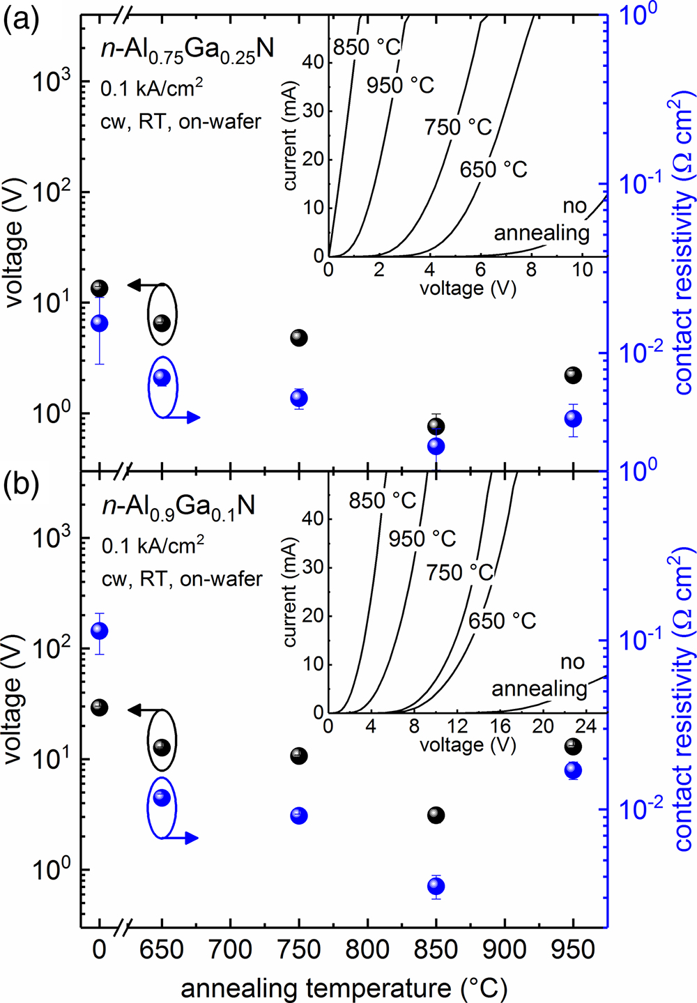
    Fig. 1. Contact resistivity and voltage evaluated at 0.1  kA/cm2 as a function of the annealing temperature for n-contacts on (a) nAl0.75Ga0.25N and on (b) nAl0.9Ga0.1N. The insets show the experimental IV curves at an electrode distance of 8 μm for different annealing temperatures.
    Experimental IV curves and contact resistivity evaluated at 0.1 kA/cm2 for n-contacts annealed at 800°C on n‐AlxGa1−xN as a function of the Al mole fraction at an electrode distance of 8 μm.
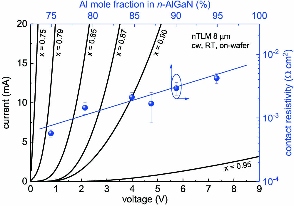
    Fig. 2. Experimental IV curves and contact resistivity evaluated at 0.1  kA/cm2 for n-contacts annealed at 800°C on nAlxGa1xN as a function of the Al mole fraction at an electrode distance of 8 μm.
    HAADF STEM images for n-contacts on (a) n‐Al0.75Ga0.25N and on (b) n‐Al0.9Ga0.1N annealed at 850°C. The inset in (a) shows a magnified image of the M/S interface with a thin interfacial AlN layer. (c) Exemplary EDXS line scan across the M/S interface marked by an arrow in (a) for n‐Al0.75Ga0.25N. The dashed line indicates the M/S position. (d) Exemplary EELS spectra for N-K and O-K edges measured at the M/S interface for n‐Al0.75Ga0.25N and for n‐Al0.9Ga0.1N.
    Fig. 3. HAADF STEM images for n-contacts on (a) nAl0.75Ga0.25N and on (b) nAl0.9Ga0.1N annealed at 850°C. The inset in (a) shows a magnified image of the M/S interface with a thin interfacial AlN layer. (c) Exemplary EDXS line scan across the M/S interface marked by an arrow in (a) for nAl0.75Ga0.25N. The dashed line indicates the M/S position. (d) Exemplary EELS spectra for N-K and O-K edges measured at the M/S interface for nAl0.75Ga0.25N and for nAl0.9Ga0.1N.
    HRTEM images of the M/S interface for (a) n‐Al0.75Ga0.25N and for (b) n‐Al0.9Ga0.1N annealed at 850°C. The lower images (c)–(f) show the FFTs of the respective marked areas in the HRTEM micrographs. The M/S interface is indicated by dashed lines.
    Fig. 4. HRTEM images of the M/S interface for (a) nAl0.75Ga0.25N and for (b) nAl0.9Ga0.1N annealed at 850°C. The lower images (c)–(f) show the FFTs of the respective marked areas in the HRTEM micrographs. The M/S interface is indicated by dashed lines.
    Experimental LIV, EQE, and WPE curves measured on-wafer for a 0.15 mm2 LED emitting at 232 nm under cw operation. The inset shows the spectral power density at 20 mA.
    Fig. 5. Experimental LIV, EQE, and WPE curves measured on-wafer for a 0.15mm2 LED emitting at 232 nm under cw operation. The inset shows the spectral power density at 20 mA.
    Luca Sulmoni, Frank Mehnke, Anna Mogilatenko, Martin Guttmann, Tim Wernicke, Michael Kneissl. Electrical properties and microstructure formation of V/Al-based n-contacts on high Al mole fraction n-AlGaN layers[J]. Photonics Research, 2020, 8(8): 1381
    Download Citation