Abstract
The electrical and structural properties of V/Al-based n-contacts on with an Al mole fraction ranging from to are investigated. Ohmic n-contacts are obtained up to with a contact resistivity of whereas for higher Al mole fraction the IV characteristics are rectifying. Transmission electron microscopy reveals a thin crystalline AlN layer formed at the metal/semiconductor interface upon thermal annealing. Compositional analysis confirmed an Al enrichment at the interface. The interfacial nitride-based layer in n-contacts on is partly amorphous and heavily contaminated by oxygen. The role and resulting limitations of Al in the metal stack for n-contacts on n-AlGaN with very high Al mole fraction are discussed. Finally, ultraviolet C (UVC) LEDs grown on and emitting at 232 nm are fabricated with an operating voltage of 7.3 V and an emission power of 120 μW at 20 mA in cw operation.1. INTRODUCTION
The formation of ohmic contacts on n-type group-III-nitride semiconductor materials is well established, especially for -GaN [1]. The basic mechanism involves the reaction of the metal contact (typically Ti or Al) with the n-type III-nitride material upon thermal annealing: N is extracted from the semiconductor layer and a continuous thin crystalline nitride-based layer (typically TiN or AlN) is formed at the metal/semiconductor (M/S) interface [2–4]. In many publications, the reduction of the contact resistivity and the subsequent onset of the ohmic behavior were attributed to the formation of this nitride-based layer [5]. As N vacancies act as donor states in n-type III-nitrides, a thin but heavily n-doped semiconductor layer is generated underneath the metal and the net carrier concentration at the interface is increased [2,6–8]. Consequently, the probability of tunneling for carriers through the thin space charge region (SCR) at the M/S interface increases as the contact resistance decreases exponentially with the doping [9].
At a higher Al mole fraction, however, the formation of ohmic contacts on n-AlGaN becomes more challenging as it is more difficult to reduce the potential barrier at the M/S interface. First, the electron affinity of AlGaN decreases with the Al mole fraction from 3.18 eV for GaN to 1.01 eV for AlN [10]. Due to the lack of appropriate low work-function metals, the Schottky barrier at the M/S interface will therefore increase with the Al mole fraction. In addition, AlGaN is more energetically stable with higher Al mole fraction, thus inhibiting the extraction of N and the formation of the heavily n-doped layer upon thermal annealing [4]. Due to the need for a transparent current spreading layer, sub-240-nm UVC LEDs require an layer with an Al molar fraction higher than [11]. Achieving ohmic n-contacts with low contact resistivities on high Al mole fraction n-AlGaN is therefore essential in order to improve the wall-plug efficiency (WPE) of deep UV LEDs. These devices are particularly interesting for applications such as gas sensing and detection of heavy metals and nitrates in natural waters and wastewaters [12–14].
Ti/Al-based metallization schemes have shown to form ohmic contacts with n-AlGaN only up to an Al molar fraction of [15]. Given the low formation enthalpy of TiN (), Ti strongly reacts with the n-AlGaN layer [5]. When increasing the Al mole fraction, Ti will then substitutionally replace Ga in the alloy leading to (i) the formation of highly defected Al-Ti-N phases, (ii) voids, and (iii) TiN protrusion islands (preferentially formed along dislocations) at the M/S interface, thus hindering the development of a uniform contact area [4,5,15,16]. Recently, Nagata et al. reported ohmic contacts on n-AlGaN up to an Al molar fraction of by using V/Al/Ni/Au-based electrodes [17]. V/Al-based metallizations have proven to provide lower contact resistivities at lower annealing temperatures compared to Ti/Al-based ones for Al mole fractions higher than 0.4 partly due to a very limited reaction with the semiconductor [15,18,19]. In this case, the generation of the heavily n-doped thin layer at the M/S interface is driven by the aluminum in the metallization scheme while the vanadium acts as an indiffusion barrier [18].
Sign up for Photonics Research TOC. Get the latest issue of Photonics Research delivered right to you!Sign up now
In this paper, the electrical and structural properties of V/Al-based n-contacts on n-AlGaN with Al molar fraction of have been systematically studied as a function of the annealing temperature. Furthermore, a model explaining the formation of n-contacts on n-AlGaN with very high Al mole fraction will be discussed.
2. EXPERIMENT
Single n-doped AlGaN layers as well as UVC LED heterostructures were grown by metalorganic vapor phase epitaxy on (0001) epitaxially laterally overgrown AlN/sapphire with dislocation densities of [20]. The heterostructure design is described in more detail elsewhere [11]. Note that the n-AlGaN layers have an optimized doping concentration in the range of as determined by secondary ion mass spectrometry for different aluminum compositions in order to reduce the layer resistivity [21]. All n-AlGaN layers have been exposed to plasma etching in an inductively coupled plasma reactive-ion-etching reactor with a pure chemistry. The n-contacts were fabricated by thermally evaporating a V/Al/Ni/Au (15/90/20/30 nm) metal stack followed by an annealing step of 1 min in an SSI Solaris 100 rapid thermal processor at annealing temperatures ranging from 650°C to 950°C. Note that the furnace is not operated under vacuum conditions, and a flowing atmosphere purges the chamber during the thermal annealing process. The contact characteristics were determined using the linear transmission line method (TLM). As the evaluation of a rectifying contact using the TLM depends on the operating point, a fixed current density of has been chosen in order to compare the different n-contacts. For ohmic contacts, the evaluated contact resistivities are evidently independent of the operating point. Finally, UVC LEDs were fabricated by thermally evaporating a Pd/Au (50/300 nm) metal stack as p-contact. The LEDs were characterized on-wafer without any active cooling by electroluminescence spectroscopy using a calibrated UV enhanced Si-photodiode and a calibrated compact optical fiber spectrometer. For cross-sectional transmission electron microscopy (TEM) analysis, single n-layer samples and were prepared using a focused ion beam technique and investigated in a JEOL 2200FS microscope equipped with an in-column energy filter. High-resolution TEM using broad parallel beam illumination (HRTEM) and high-angle annular dark-field scanning TEM (HAADF STEM) in combination with energy-dispersive X-ray spectroscopy (EDXS) and electron energy loss spectroscopy (EELS) were performed to reveal the structure and the compositional uniformity of the M/S interface after annealing and to relate microstructure with electrical characteristics.
3. RESULTS AND DISCUSSION
Figure 1 shows the contact resistivity and voltage evaluated at and averaged across each wafer as a function of the annealing temperature for n-contacts on [Fig. 1(a)] and on [Fig. 1(b)] single layers. For both Al mole fractions, a minimum in contact resistivity is reached around 850°C, i.e., for and for . Annealing at higher temperatures results in a degradation of the contacts. The experimental IV curves for different annealing temperatures are displayed in the insets of Fig. 1. The as-deposited n-contacts (no annealing) are clearly rectifying. By increasing the annealing temperature, the IV characteristics are less rectifying, reach a minimum in terms of contact resistivity and voltage around 850°C, and then increase again the rectifying behavior for higher temperatures. Note that the IV characteristics of are linear after annealing at 850°C as the n-contacts are ohmic, whereas the n-contacts on still exhibit a moderate Schottky behavior. This suggests that the ohmic contact formation mechanism occurs at the same temperature of 850°C for both Al mole fractions. Since a higher Al mole fraction implies a higher potential barrier at the interface, this observation supports the idea that carrier tunneling through a thin potential barrier due to a heavily n-doped thin semiconductor layer is the underlying mechanism of n-contact formation in n-type III-nitrides upon thermal annealing [22].
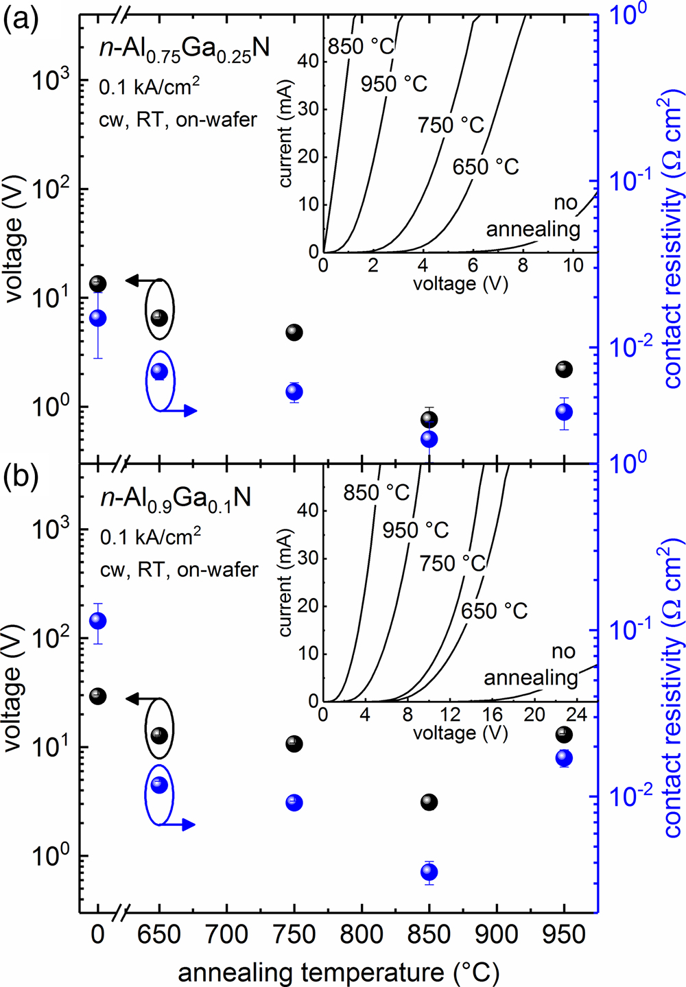
Figure 1.Contact resistivity and voltage evaluated at as a function of the annealing temperature for n-contacts on (a) and on (b) . The insets show the experimental IV curves at an electrode distance of 8 μm for different annealing temperatures.
By carefully adjusting the surface treatment of the plasma-etched n-layers and the thermal annealing recipe of the deposited electrodes, it was possible to further reduce the contact resistivities and to obtain less rectifying n-contacts even at lower annealing temperatures. In Fig. 2, the electrical characteristics of optimized n-contacts on with Al mole fractions ranging from up to are summarized. N-contacts on are ohmic after annealing at 800°C. When increasing the Al mole fraction, the rectifying behavior increases and the current level decreases accordingly. The voltage evaluated at is 0.15 V for and increases rapidly up to 6.2 V for . The contact resistivity evaluated at undergoes proportionally a smaller increase from for up to for . Typically, the reported values of contact resistivities for ohmic contacts on n-AlGaN are in the range of up to an Al molar fraction of 0.7 and increase drastically to on n-AlN [17].

Figure 2.Experimental IV curves and contact resistivity evaluated at for n-contacts annealed at 800°C on as a function of the Al mole fraction at an electrode distance of 8 μm.
This raises the question why the rectifying behavior increases so sharply with the Al mole fraction. In case of thermionic emission, an increase in Al mole fraction would lead to an increase in the Schottky barrier height and thus to an increase in the n-electrode resistance, whereas for tunneling emission, an increase in Al mole fraction would not lead to an increase in the n-contact resistance as carrier tunneling is virtually independent of the potential barrier height at the M/S interface. According to Grabowski et al., the decrease in electron affinity for AlGaN with an Al mole fraction of up to is rather modest (i.e., ) and therefore can only partly explain the large increase in the rectifying behavior observed in Fig. 2 [23]. Our experimental observation suggests that the formation of n-contacts on n-AlGaN is due to a reduction of the SCR allowing for efficient carrier tunneling. In this case, the potential barrier thickness strongly depends on the doping concentration near the interface [9]. The increasingly rectifying behavior observed with increasing Al mole fraction indicates then that N-vacancy formation becomes less efficient. This prevents the formation of a heavily n-doped thin semiconductor layer underneath the electrode. Since N atoms create a more stable compound with Al than with Ga due to the lower formation enthalpy of AlN () in comparison to GaN (), Al in the metal stack no longer reacts extensively with the underlying n-AlGaN layers [3,5]. This is in agreement with reports showing that the dissociation of nitrides from the semiconductor surface occurs at higher activation energies for AlN (4.4 eV) than for GaN (3.8 eV) [24].
In order to reveal the underlying mechanism of contact formation, exemplary HAADF STEM images of annealed n-contacts on and on are shown in Fig. 3. The phase formation in both n-contacts is very similar and the M/S interface is smooth with no protrusions or metal indiffusion into the AlGaN layer. On the microscale, EDXS analysis reveals three different phases that are not in direct contact with the n-AlGaN surface: Au-Al, Ni-Al, and V-Al-Au. On the nanoscale, however, a thin interfacial layer is observed at the M/S interface. Note that some inhomogeneities in the composition and structure of the interfacial layer can be observed in both samples. Three regions with different materials appearing in contact to the AlGaN semiconductor were observed: (i) regions with a thin (0.5–5 nm) AlN layer; (ii) regions with a thick Al(O)N layer (5–20 nm); (iii) regions with a Au-containing phase. For , most of the interfacial area () shows a thin AlN layer that due to its small thickness is magnified in the inset of Fig. 3(a). The amount of thick Al(O)N area increases drastically with increasing Al mole fraction. For , about 50% of the interfacial area is covered by a thick, partly amorphous Al(O)N layer and only 10% by a thin AlN layer as depicted by the discontinuous dark interfacial layer in Fig. 3(b). Note that no clear correlation is observed between the presence of the interfacial AlN layer and one of the three metallic phases Au-Al, Ni-Al, and V-Al-Au.
Figure 3.HAADF STEM images for n-contacts on (a) and on (b) annealed at 850°C. The inset in (a) shows a magnified image of the M/S interface with a thin interfacial AlN layer. (c) Exemplary EDXS line scan across the M/S interface marked by an arrow in (a) for . The dashed line indicates the M/S position. (d) Exemplary EELS spectra for N-K and O-K edges measured at the M/S interface for and for .
An EDXS line scan across the M/S interface shows an increasing Al-K edge intensity in the thin AlN layer, whereas the intensity of other metal peaks decreases in this region [Fig. 3(c)]. These results prove the generally discussed model of Al consumption from the metal stack through the V barrier and N extraction from n-AlGaN to form a thin interfacial AlN layer. Luther et al. also observed a stronger Al signal near the interface consistent with the presence of a 2–3 nm thick pseudomorphic AlN layer under tensile strain [2]. In this interfacial region, V and Au signals decrease down to the detection limit. No Ga outdiffusion has occurred; the small Ga-K signal detected outside of the n-AlGaN in Fig. 3(c) is an artifact due to semiconductor resputtering during the sample preparation for TEM investigations. Comparable EDXS line scans were observed for thicker interfacial layers on but with a higher O-K edge intensity as depicted by the EELS spectra in Fig. 3(d). Similar Al(O)N regions have been previously published for V/Al/V/Au n-contacts on [15]. Note that some oxidation takes place also in 5-nm-thick AlN regions on ; however, it decreases with decreasing thickness of the interfacial layer according to EDXS and EELS analyses. Most likely, only a thin interfacial AlN layer may provide good contact properties. A possible initial presence of a surface oxide on the more Al-rich layer can facilitate the Al(O)N formation. However, no clear oxygen signal was detected on as-deposited metal stacks using EELS analysis, indicating that the oxygen concentration is well below 1 at. %. Our previous X-ray photoelectron spectroscopy studies showed an enhanced oxygen contamination on plasma-etched surfaces after thermal annealing under atmosphere prior to the deposition of metal layers [25]. This suggests that the thermal annealing atmosphere acts as an external oxygen source and is therefore the dominant oxidation process. When the Al mole fraction in the n-AlGaN layer increases, the reaction of Al in the metal stack with the AlGaN layers is hindered due to a less effective N-vacancy formation, thus leaving the interfacial layer more exposed to oxidation upon thermal annealing. The larger thickness of the interfacial layer on is then attributed rather to a stronger oxidation during the contact annealing process resulting in the formation of defective Al(O)N and in a persistent rectifying behavior despite the minimum in contact conductivity shown in Fig. 1.
HRTEM images in Fig. 4 show the presence of a well-aligned interfacial AlN layer with a thickness of about 5 nm on [Fig. 4(a)] and of a highly defective Al(O)N layer with a thickness of about 10 nm on [Fig. 4(b)]. As for the HAADF STEM images, the transition from the semiconductor to the metal is smooth, in good agreement with the limited reaction of V-based n-contacts on reported by Miller et al. [15]. The fast Fourier transforms (FFTs) of the image areas (c, d, e, f) framed in Figs. 4(a) and 4(b) indicate the higher crystal quality of the interfacial AlN layer on matching the lattice plane pattern of the AlGaN layer underneath. In comparison, the FFTs of the thick Al(O)N layer on show the appearance of additional spatial frequencies [Fig. 4(e)], suggesting the possible formation of a superstructure. This can be formed either due to an enhanced, although ordered, incorporation of oxygen atoms and/or to a spatial ordering of point defects [26]. With increasing Al(O)N thickness, the ordered atom arrangement is lost and the upper layer regions appear nearly amorphous, which is visible from a diffuse intensity ring in Fig. 4(f). This indicates that the oxygen contamination is likely to originate from the thermal annealing atmosphere rather than from the underlying n-AlGaN layers, as previously discussed. As HRTEM images of the as-deposited metal stack exhibit only vanadium in contact with the semiconductor surface (not shown here), we conclude that the reaction of Al and n-AlGaN, forming a thin crystalline AlN layer at the interface and a highly N-deficient AlGaN layer inside the semiconductor, accompanies the reduction of the rectifying behavior and of the contact resistivity upon thermal annealing observed in Fig. 1. This is in agreement with the observations of Wang et al. attributing the transition to ohmic behavior with the formation of a 2-nm-thick interfacial TiN layer for Ti/Al/Mo/Au metallization on while analyzing cross-sectional TEM images at various annealing temperatures ranging from 400°C up to 950°C [16].
Figure 4.HRTEM images of the M/S interface for (a) and for (b) annealed at 850°C. The lower images (c)–(f) show the FFTs of the respective marked areas in the HRTEM micrographs. The M/S interface is indicated by dashed lines.
A few considerations can be made regarding this heavily n-doped layer. First of all, the n-AlGaN samples employed for the present study have a Si-doping concentration of and hence the N-vacancy annealing-induced doping is expected to lead to a much higher donor concentration [21]. In Fig. 4(a), an extremal case is shown, in which the thickness of the interfacial layer locally reaches its maximum of about 5 nm. More commonly, the thickness of the interfacial AlN layer is and all N atoms in this layer need to come from the n-AlGaN underneath. The density of atoms in ideal wurtzite AlN is , which means a density of N atoms of [27]. Assuming a 1% N depletion (i.e., donors), the heavily n-doped layer would be around 100 nm thick. This is an extreme case as the crystal structure of AlGaN will be probably severely damaged if 1% of the total number of atoms turns into N vacancies. Motayed et al. assumed a donor concentration of extending around 10 nm inside n-GaN generated by only a few monolayers of TiTaN after annealing Ta/Ti/Ni/Au n-contacts [8]. However, it is very likely that both the N depletion thickness and the amount of donors are overestimated due to (i) imperfectly balanced stoichiometry between Al and N atoms of the binary compound AlN (some M/S regions are also oxygen contaminated), (ii) spatially inhomogeneous thickness of the interfacial layer (some M/S regions do not contain the interfacial layer), and (iii) formation of N vacancy complexes with a different electrical behavior (e.g., divacancies) [28]. Moreover, as suggested by Luther et al., probably the interfacial AlN layer is highly defective, thus favoring carrier tunneling through the n-contact [2].
In conclusion, the poor electrical properties of n-contacts when increasing the Al mole fraction in the n-AlGaN layers are due to the difficulty to generate a sufficient density of donors at the M/S interface necessary for the field emission in a tunneling contact. This is caused by material limitations as well as limitations in epitaxy and microfabrication process. On the material side, the electron affinity decreases and drops down to 1.01 eV for AlN leading to a higher Schottky barrier for electrons [10]. On the epitaxial side, self-compensation effects of the Si dopant limit the number of available Si-based donors leading to a thicker Schottky barrier for electrons [29,30]. This drastically reduces the charge carrier density available at the interface. In fact, Mehnke et al. observed a sharp increase in sheet resistivity when increasing the Al mole fraction in n-AlGaN from up to and for -AlN, similar to the increase in contact resistance shown in Fig. 2 and reported in Refs. [17,29,30]. On the microfabrication side, the development of a heavily n-doped layer at the interface upon thermal annealing is limited by (i) stronger N bond in AlGaN hindering the N vacancy formation and by (ii) less favorable formation energy of donor-like N vacancies leading also to a thicker Schottky barrier for electrons. As a consequence of mechanism (i), an additional barrier is introduced at the M/S interface by the formation of a thick defective Al(O)N layer. Regarding mechanism (ii), it was reported recently that nitrogen vacancies in AlN behave as amphoteric defects changing from donor to acceptor without a stable neutral state: from first-principles calculations the charge switch occurs at very shallow Fermi level positions within the bandgap, i.e., close to the conduction band, where the Fermi level is expected for n-AlGaN with high Al mole fraction [31,32]. Therefore, the most effective mechanism to thin the Schottky barrier at the M/S interface (i.e., formation of donor-like N vacancies) in III-nitride-based devices is no longer active for such high Al mole fractions.
Finally, UVC LEDs with an emission wavelength of 232 nm are fabricated to investigate the reliability and performance of these optimized n-contacts in terms of operating voltage. Full transparency to the emitted light toward the substrate while preserving high sheet conductivity and low contact resistivity is ensured with an current spreading layer [11]. The n-contact resistivity and voltage evaluated by TLM at are and 2.1 V, respectively. Light crrent voltage (LIV) curves measured on-wafer for a device are shown in Fig. 5 under cw operation without active cooling. The operating voltage and emission power are 7.3 V and 120 μW, respectively, at 20 mA and increase up to 9.9 V and 420 μW at 100 mA close to the thermal rollover due to Joule heating. The maximum external quantum efficiency (EQE) and WPE are 0.12% and 0.08%, respectively, measured on-wafer. Previously, Moe et al. reported 10.4 V at 100 mA for Ti/Al/Ni/Au n-contacts on in 233 nm LEDs grown on AlN bulk substrates [33].
Figure 5.Experimental LIV, EQE, and WPE curves measured on-wafer for a LED emitting at 232 nm under cw operation. The inset shows the spectral power density at 20 mA.
4. CONCLUSION
In summary, we have shown how the contact characteristics on n-AlGaN with high Al mole fraction are intimately related to the formation of a thin crystalline AlN layer at the M/S interface upon thermal annealing. It was possible to achieve ohmic n-contacts on n-AlGaN up to an Al mole fraction of 0.75. For higher Al mole fractions, the rectifying behavior prevails, and the interfacial AlN layer becomes more amorphous and heavily oxygen-contaminated. By carefully optimizing the annealing conditions, we fabricated UVC LEDs emitting at 232 nm grown on with an operating voltage of 7.3 V and an emission power of 120 μW at 20 mA in cw operation. We have shown how it becomes increasingly difficult to achieve highly conductive n-layers and n-contacts on wide-bandgap semiconductors such as n-AlGaN with high Al content typically used for very deep UV LEDs. The limited number of available donors due to several material limitations is the reason behind the high operating voltages. On the microfabrication process side, the lack of an efficiently heavily doped n-layer created upon thermal annealing at the M/S interface inhibits the thinning of the potential barrier, thus hindering carrier injection. This is in fact a specific material limitation of n-AlGaN layers with high Al mole fraction: on one side, an element (preferably highly conductive as a metal) able to form more energetically favorable nitrides than TiN or AlN is required; on the other side, a new physical mechanism able to form higher donor concentrations than the N-vacancy one needs to discover.
Acknowledgment
Acknowledgment. The authors would like to thank Sylvia Hagedorn (Ferdinand-Braun-Institut, Leibniz-Institut für Höchstfrequenztechnik, Berlin) for providing ELO AlN/sapphire templates and Markus Weyers (Ferdinand-Braun-Institut, Leibniz-Institut für Höchstfrequenztechnik, Berlin) for critically reading the manuscript.
References
[1] G. Greco, F. Iucolano, F. Roccaforte. Ohmic contacts to gallium nitride materials. Appl. Surf. Sci., 383, 324-345(2016).
[2] B. P. Luther, J. M. DeLucca, S. E. Mohney, R. F. Karlicek. Analysis of a thin AlN interfacial layer in Ti/Al and Pd/Al ohmic contacts to n-type GaN. Appl. Phys. Lett., 71, 3859-3861(1997).
[3] S. Ruvimov, Z. Liliental-Weber, J. Washburn, D. Qiao, S. S. Lau, P. K. Chu. Microstructure of Ti/Al ohmic contacts for n-AlGaN. Appl. Phys. Lett., 73, 2582-2584(1998).
[4] B. V. Daele, G. V. Tendeloo, W. Ruythooren, J. Derluyn, M. R. Leys, M. Germain. The role of Al on ohmic contact formation on n-type GaN and AlGaN/GaN. Appl. Phys. Lett., 87, 061905(2005).
[5] L. Wang, F. M. Mohammed, I. Adesida. Differences in the reaction kinetics and contact formation mechanisms of annealed Ti/Al/Mo/Au ohmic contacts on n-GaN and AlGaN/GaN epilayers. J. Appl. Phys., 101, 013702(2007).
[6] C. G. Van de Walle, C. Stampfl, J. Neugebauer, M. D. McCluskey, N. M. Johnson. Doping of AlGaN alloys. MRS Int. J. Nitride Semicond. Res., 4, 890-901(1999).
[7] A. Motayed, R. Bathe, M. C. Wood, O. S. Diouf, R. D. Vispute, S. N. Mohammad. Electrical, thermal, and microstructural characteristics of Ti/Al/Ti/Au multilayer ohmic contacts to n-type GaN. J. Appl. Phys., 93, 1087-1094(2002).
[8] A. Motayed, K. A. Jones, M. A. Derenge, M. C. Wood, D. N. Zakharov, Z. Liliental-Weber, D. J. Smith, A. V. Davydov, W. T. Anderson, A. A. Iliadis, S. Noor Mohammad. Electrical, microstructural, and thermal stability characteristics of Ta/Ti/Ni/Au contacts to n-GaN. J. Appl. Phys., 95, 1516-1524(2004).
[9] M. Grundmann. The Physics of Semiconductors: An Introduction Including Devices and Nanophysics(2006).
[10] P. G. Moses, M. Miao, Q. Yan, C. G. Van de Walle. Hybrid functional investigations of band gaps and band alignments for AlN, GaN, InN, and InGaN. J. Chem. Phys., 134, 084703(2011).
[11] F. Mehnke, L. Sulmoni, M. Guttmann, T. Wernicke, M. Kneissl. Influence of light absorption on the performance characteristics of UV LEDs with emission between 239 and 217 nm. Appl. Phys. Express, 12, 012008(2019).
[12] F. Mehnke, M. Guttmann, J. Enslin, C. Kuhn, C. Reich, J. Jordan, S. Kapanke, A. Knauer, M. Lapeyrade, U. Zeimer, H. Krüger, M. Rabe, S. Einfeldt, T. Wernicke, H. Ewald, M. Weyers, M. Kneissl. Gas sensing of nitrogen oxide utilizing spectrally pure deep UV LEDs. IEEE J. Sel. Top. Quantum Electron., 23, 29-36(2017).
[13] M. Yaman, S. Bakirdere. Identification of chemical forms of lead, cadmium and nickel in sewage sludge of waste water treatment facilities. Microchim. Acta, 141, 47-54(2003).
[14] O. Thomas, S. Gallot, N. Mazas. Ultraviolet multiwavelength absorptiometry (UVMA) for the examination of natural waters and wastewaters. Fresenius J. Anal. Chem., 338, 238-240(1990).
[15] M. A. Miller, B. H. Koo, K. H. A. Bogart, S. E. Mohney. Ti/Al/Ti/Au and V/Al/V/Au contacts to plasma-etched n-Al0.58Ga0.42N. J. Electron. Mater., 37, 564-568(2008).
[16] L. Wang, F. M. Mohammed, I. Adesida. Formation mechanism of ohmic contacts on AlGaN/GaN heterostructure: electrical and microstructural characterizations. J. Appl. Phys., 103, 093516(2008).
[17] N. Nagata, T. Senga, M. Iwaya, T. Takeuchi, S. Kamiyama, I. Akasaki. Reduction of contact resistance in V-based electrode for high AlN molar fraction n-type AlGaN by using thin SiNx intermediate layer. Phys. Status Solidi C, 14, 1600243(2016).
[18] M. Lapeyrade, A. Muhin, S. Einfeldt, U. Zeimer, A. Mogilatenko, M. Weyers, M. Kneissl. Electrical properties and microstructure of vanadium-based contacts on ICP plasma etched n-type AlGaN:Si and GaN:Si surfaces. Semicond. Sci. Technol., 28, 125015(2013).
[19] K. Mori, K. Takeda, T. Kusafuka, M. Iwaya, T. Takeuchi, S. Kamiyama, I. Akasaki, H. Amano. Low-ohmic-contact-resistance V-based electrode for n-type AlGaN with high AlN molar fraction. Jpn. J. Appl. Phys., 55, 05FL03(2016).
[20] G. Kusch, M. Nouf-Allehiani, F. Mehnke, C. Kuhn, P. R. Edwards, T. Wernicke, A. Knauer, V. Kueller, G. Naresh-Kumar, M. Weyers, M. Kneissl, C. Trager-Cowan, R. W. Martin. Spatial clustering of defect luminescence centers in Si-doped low resistivity Al0.82Ga0.18N. Appl. Phys. Lett., 107, 072103(2015).
[21] G. Kusch, F. Mehnke, J. Enslin, P. R. Edwards, T. Wernicke, M. Kneissl, R. W. Martin. Analysis of doping concentration and composition in wide bandgap AlGaN:Si by wavelength dispersive x-ray spectroscopy. Semicond. Sci. Technol., 32, 035020(2017).
[22] X. A. Cao, H. Piao, S. F. LeBoeuf, J. Li, J. Y. Lin, H. X. Jiang. Effects of plasma treatment on the ohmic characteristics of Ti/Al/Ti/Au contacts to n-AlGaN. Appl. Phys. Lett., 89, 082109(2006).
[23] S. P. Grabowski, M. Schneider, H. Nienhaus, W. Mönch, R. Dimitrov, O. Ambacher, M. Stutzmann. Electron affinity of AlxGa1-xN (0001) surfaces. Appl. Phys. Lett., 78, 2503-2505(2001).
[24] J. Hong, J. W. Lee, J. D. MacKenzie, S. M. Donovan, C. R. Abernathy, S. J. Pearton, J. C. Zolper. Comparison of GaN, InN and AlN powders for susceptor-based rapid annealing of group III nitride materials. Semicond. Sci. Technol., 12, 1310-1318(1997).
[25] M. Lapeyrade, S. Alamé, J. Glaab, A. Mogilatenko, R.-S. Unger, C. Kuhn, T. Wernicke, P. Vogt, A. Knauer, U. Zeimer, S. Einfeldt, M. Weyers, M. Kneissl. Effect of Cl2 plasma treatment and annealing on vanadium based metal contacts to Si-doped Al0.75Ga0.25N. J. Appl. Phys., 122, 125701(2017).
[26] S. Mohn, N. Stolyarchuk, T. Markurt, R. Kirste, M. P. Hoffmann, R. Collazo, A. Courville, R. D. Felice, Z. Sitar, P. Vennéguès, M. Albrecht. Polarity control in group-III nitrides beyond pragmatism. Phys. Rev. Appl., 5, 054004(2016).
[27] M. Kneissl, J. Rass. III-Nitride Ultraviolet Emitters—Technology and Applications, 227(2016).
[28] M. A. Reshchikov, H. Morkoç. Luminescence properties of defects in GaN. J. Appl. Phys., 97, 061301(2005).
[29] F. Mehnke, T. Wernicke, H. Pingel, C. Kuhn, C. Reich, V. Kueller, A. Knauer, M. Lapeyrade, M. Weyers, M. Kneissl. Highly conductive n-AlxGa1-xN layers with aluminum mole fractions above 80%. Appl. Phys. Lett., 103, 212109(2013).
[30] F. Mehnke, X. T. Trinh, H. Pingel, T. Wernicke, E. Janzén, N. T. Son, M. Kneissl. Electronic properties of Si-doped AlxGa1-xN with aluminum mole fractions above 80%. J. Appl. Phys., 120, 145702(2016).
[31] D. F. Hevia, C. Stampfl, F. Viñes, F. Illas. Microscopic origin of n-type behavior in Si-doped AlN. Phys. Rev. B, 88, 085202(2013).
[32] Q. Yan, A. Janotti, M. Scheffler, C. G. Van de Walle. Origins of optical absorption and emission lines in AlN. Appl. Phys. Lett., 105, 111104(2014).
[33] C. G. Moe, S. Sugiyama, J. Kasai, J. R. Grandusky, L. J. Schowalter. AlGaN light-emitting diodes on AlN substrates emitting at 230 nm. Phys. Status Solidi A, 215, 1700660(2018).

