• Journal of Semiconductors
  • Vol. 43, Issue 3, 032701 (2022)
Zhe Yin1, Min Hu1, Jun Liu2、3, Hao Fu1, Zhijie Wang2、3、4, and Aiwei Tang1
Author Affiliations
  • 1Key Laboratory of Luminescence and Optical Information, Ministry of Education, School of Science, Beijing Jiaotong University, Beijing 100044, China
  • 2Key Laboratory of Semiconductor Materials Science, Institute of Semiconductors, Chinese Academy of Sciences, Beijing 100083, China
  • 3Beijing Key Laboratory of Low Dimensional Semiconductor Materials and Devices, Institute of Semiconductors, Chinese Academy of Sciences, Beijing 100083, China
  • 4College of Materials Science and Opto-Electronic Technology, University of Chinese Academy of Sciences, Beijing 100049, China
  • show less
    DOI: 10.1088/1674-4926/43/3/032701 Cite this Article
    Zhe Yin, Min Hu, Jun Liu, Hao Fu, Zhijie Wang, Aiwei Tang. Tunable crystal structure of Cu–Zn–Sn–S nanocrystals for improving photocatalytic hydrogen evolution enabled by copper element regulation[J]. Journal of Semiconductors, 2022, 43(3): 032701 Copy Citation Text show less
    (Color online) (a) Schematic illustration of one-pot synthesis of CZTS nanocrystals. XRD patterns of CZTS nanocrystals obtained at (b) low Cu content, (c) high Cu content. (d) TEM images of hexagonal wurtzite CZTS. The inset is an enlarged view. (e) SAED pattern of hexagonal wurtzite CZTS. (f) HRTEM images of hexagonal wurtzite CZTS nanocrystals in (002) crystal plane and (g) in (101) crystal plane.
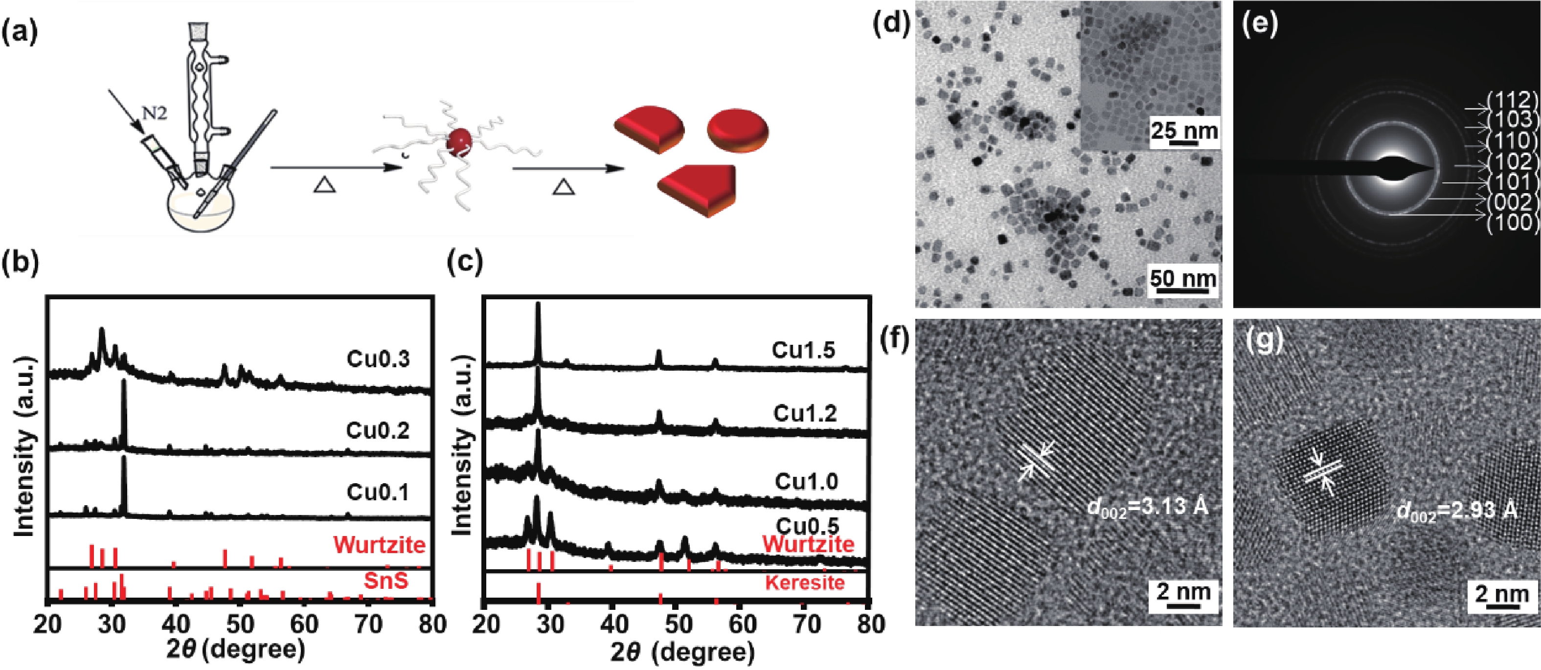
    Fig. 1. (Color online) (a) Schematic illustration of one-pot synthesis of CZTS nanocrystals. XRD patterns of CZTS nanocrystals obtained at (b) low Cu content, (c) high Cu content. (d) TEM images of hexagonal wurtzite CZTS. The inset is an enlarged view. (e) SAED pattern of hexagonal wurtzite CZTS. (f) HRTEM images of hexagonal wurtzite CZTS nanocrystals in (002) crystal plane and (g) in (101) crystal plane.
    (Color online) (a) SEM-EDS element distribution diagram of hexagonal wurtzite CZTS nanocrystals. (b) The cation percentages of CTZS nanocrystals obtained from EDS results. XPS signals of (c) Cu, (d) Sn, (e) Zn, and (f) S elements in hexagonal wurtzite CZTS nanocrystals.
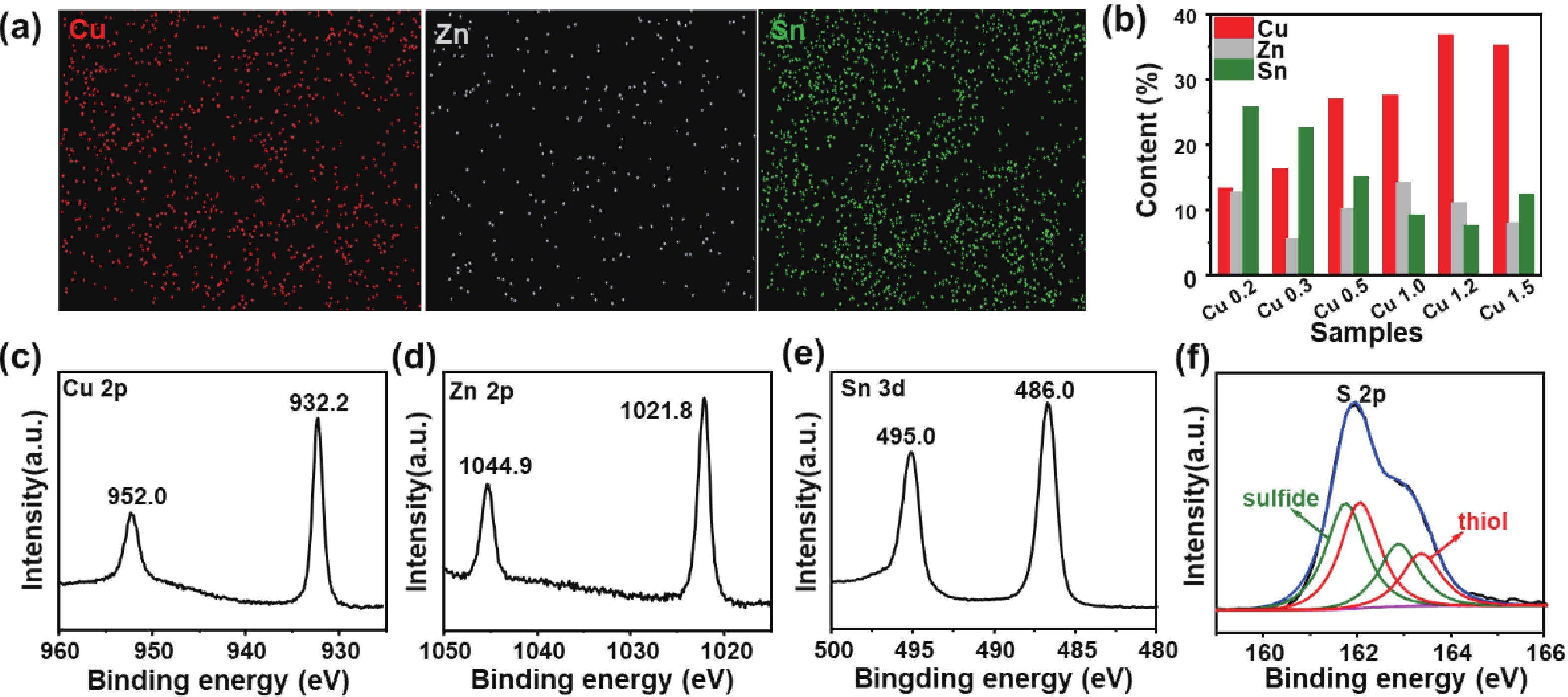
    Fig. 2. (Color online) (a) SEM-EDS element distribution diagram of hexagonal wurtzite CZTS nanocrystals. (b) The cation percentages of CTZS nanocrystals obtained from EDS results. XPS signals of (c) Cu, (d) Sn, (e) Zn, and (f) S elements in hexagonal wurtzite CZTS nanocrystals.
    (Color online) (a) Diffuse reflectance spectra and (b) the plots of (αhv)2 versus the photon energy of CZTS nanocrystals with different Cu content. UPS spectra of (c) high-binding energy secondary-electron cutoff and (d) valence-band edge regions of hexagonal wurtzite CZTS nanocrystals. (e) Energy level structure diagram of hexagonal wurtzite CZTS nanocrystals.
    Fig. 3. (Color online) (a) Diffuse reflectance spectra and (b) the plots of (αhv)2 versus the photon energy of CZTS nanocrystals with different Cu content. UPS spectra of (c) high-binding energy secondary-electron cutoff and (d) valence-band edge regions of hexagonal wurtzite CZTS nanocrystals. (e) Energy level structure diagram of hexagonal wurtzite CZTS nanocrystals.
    (Color online) (a) Photocurrent of CZTS nanocrystals with different Cu content. (b) Impedance spectra of CZTS nanocrystals with different Cu content. (c) Photocatalytic hydrogen evolution for hydrogen amount variation with time. (d) Photocatalytic hydrogen production rates.
    Fig. 4. (Color online) (a) Photocurrent of CZTS nanocrystals with different Cu content. (b) Impedance spectra of CZTS nanocrystals with different Cu content. (c) Photocatalytic hydrogen evolution for hydrogen amount variation with time. (d) Photocatalytic hydrogen production rates.
    SampleEcut-off(eV) Eonset(eV) VBM (eV) Band gap (eV) CBM (eV)
    Wurtzite CZTS17.681.284.821.743.08
    Table 1. Summary of the energy level information of wurtzite CZTS nanocrystals.
    Zhe Yin, Min Hu, Jun Liu, Hao Fu, Zhijie Wang, Aiwei Tang. Tunable crystal structure of Cu–Zn–Sn–S nanocrystals for improving photocatalytic hydrogen evolution enabled by copper element regulation[J]. Journal of Semiconductors, 2022, 43(3): 032701
    Download Citation