
Zhe Yin, Min Hu, Jun Liu, Hao Fu, Zhijie Wang, Aiwei Tang. Tunable crystal structure of Cu–Zn–Sn–S nanocrystals for improving photocatalytic hydrogen evolution enabled by copper element regulation[J]. Journal of Semiconductors, 2022, 43(3): 032701
- Journal of Semiconductors
- Vol. 43, Issue 3, 032701 (2022)
Abstract
1. Introduction
Hydrogen energy is a sustainable and clean energy source because it only produces water with no harmful emission for applications[
In this paper, we presented the controllable synthesis of quaternary CZTS semiconductor nanocrystals and demonstrated its applications in the photocatalytic evolution, with emphasis on the regulation of Cu content for improving photocatalytic performance. Pure hexagonal wurtzite CZTS nanocrystals were successfully synthesized through regulating the Cu content, the surface ligand, and reaction temperature. The photoelectrical and photocatalytic properties of the CZTS nanocrystals with different crystal phases for hydrogen production were compared and studied in depth. Specifically, the effects of Cu content on the band gap of CZTS nanocrystals and the photocatalytic hydrogen evolution performance were concluded.
2. Experimental methods
2.1. Synthesis
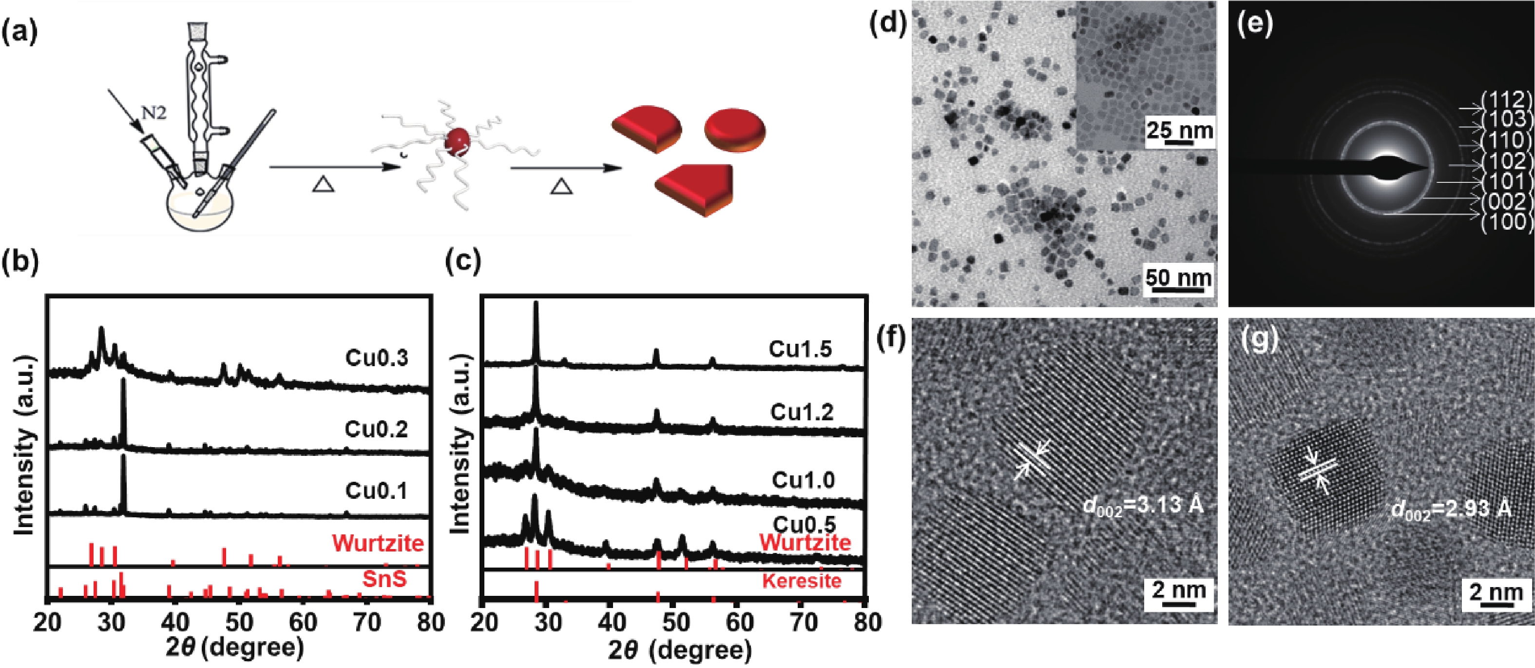
A series of quaternary CZTS nanocrystals were synthesized by a one-pot method as shown in Fig. 1(a). Firstly, the precursors (Cu(acac)2 and Zn(acac)2) were dispersed in the oleylamine (OM), and then the reaction mixture was purged with nitrogen under magnetic stirring. Afterward, the reaction mixture was heated to 130 °C slowly and then kept at this temperature for 30 min till the precursor was fully dissolved. Then, a mixed solvent containing anhydrous SnCl4 and dodecanethiol (DDT) was injected into the system, and the reaction system was continuously stirred for 30 min to realize the full dissolving of precursors. Subsequently, the system started to heat up with the reaction temperature of 240 °C. After reaching the target reaction temperature, the system was kept for 120 min. Finally, after the reaction was over, the system was naturally cooled to room temperature under the protection of nitrogen after the removal of the heating source. Post-treatment of the reaction product was as follows: the as-obtained CIZS NCs were precipitated through the addition of dichloromethane and ethanol by a centrifuge. The above procedure was repeated four times for purification and then the precipitate was collected. At last, the sample was dissolved in dichloromethane to obtain a liquid sample, and then it was treated with a freeze dryer for 24 h to obtain a solid powder.
![]()
Figure 1.(Color online) (a) Schematic illustration of one-pot synthesis of CZTS nanocrystals. XRD patterns of CZTS nanocrystals obtained at (b) low Cu content, (c) high Cu content. (d) TEM images of hexagonal wurtzite CZTS. The inset is an enlarged view. (e) SAED pattern of hexagonal wurtzite CZTS. (f) HRTEM images of hexagonal wurtzite CZTS nanocrystals in (002) crystal plane and (g) in (101) crystal plane.
2.2. Photocatalytic hydrogen reaction
2.2.1. Pretreatment of CZTS nanocrystals
The nanocrystal solution was dropped to the 3-mercaptopropionic acid solution (3%), and then it was kept stirring for 10 h in dark for transferring the samples from the oil phase to the aqueous phase. The mixture was centrifuged at high speed, and then the as-obtained samples were dissolved in ethanol. After that, methanol was added to precipitate the samples and the solution was centrifuged again. The above process was repeated 5 times. Then the precipitation was dissolved in water and centrifuged, which was repeated 3 times. Finally, the precipitation was dissolved in deionized water and lyophilized for 24 h to obtain the powder.
2.2.2. Photocatalytic test
A photocatalytic hydrogen reaction was conducted in glassware from Perfectlight Inc and the hydrogen measurements were carried out on a Shimadzu GC2014 under PM 100D xenon lamp of 500 W. The cavitation sacrificial agent (0.3 M Na2S∙9H2O and 0.3 M Na2SO3) was added to 100 mL deionized water and it was stirred for 20 min. Next, 20 mg of the powder was ultrasonically dissolved in this solution. All air was exhausted to ensure that the entire photocatalytic system was in vacuum. The temperature of the system was kept at 5 ± 0.1 °C by circulating cooling water. A 500 W xenon lamp (PM 100D) was used to simulate the sunlight. When the xenon lamp was turned on to illuminate the system, the timing was started. The photocatalytic hydrogen evolution continued for 4 h. The hydrogen production was collected every 0.5 h automatically, and it was measured by gas chromatography (Shimadzu GC2014).
2.3. Characterization
X-ray diffraction (XRD) patterns were recorded on a Bruker D8X diffractometer using a Cu Kα radiation source (λ = 1.54056 Å). Transmission electron microscopy (TEM) images were obtained from a JEM-1400 transmission electron microscope with a voltage of 80 kV. High-resolution TEM (HRTEM) images and selected area electron diffraction (SAED) were recorded on a JEM-2010. Scanning electron microscopy-energy dispersive X-ray spectroscopy (SEM-EDS) was recorded on a Hitachi S4800 with a voltage of 15 kV. X-ray photoelectron spectroscopy (XPS) was recorded on a Thermo ESCALAB 250Xi spectrometer with a 300 W Al Kα radiation source. All binding energies for different elements were calibrated to the C 1s line at 284.8 eV. The XPS results were analyzed by XPSPEAK41 software. UV–Vis diffuse reflectance spectroscopy was recorded on a Varian 5000 spectrophotometer with BaSO4 as a reference. Ultraviolet photoemission spectroscopy (UPS) was recorded on an Axis Ultra DLD spectrometer. Photocurrent and electrochemical impedance spectroscopy (EIS) was recorded on a CHI 660D electrochemical workstation.
3. Results and discussion
3.1. Crystal structure with regulated Cu content
The Cu content in the synthesis process is important for controlling its crystal phase, thus improving its photoelectric performance. Kesterite and hexagonal wurtzite phases are the most common phases of CZTS nanocrystals. The stability of the phase is closely related to its component content, especially Cu content. Researchers usually adjusted the composition of nanocrystals by changing the type or concentration of precursors, which would influence their crystal structure and morphology as well[
Fig. 1(c) shows the XRD pattern of the samples with high Cu content, with Cu0.5, Cu1.0, Cu1.2, and Cu1.5 samples. Comparing with the standard powder diffraction file, it is found that the Cu0.5 and Cu1.0 samples are hexagonal wurtzite CZTS nanocrystals without other impurity phases. As the Cu content continues to increase, the diffraction peaks of the kesterite gradually increase. When the Cu content reaches 1.5 mmol, the crystal phase changes from the main phase of hexagonal wurtzite to the main kesterite phase. The Cu1.5 sample has mixed phases of kesterite and wurtzite, in which the kesterite phase is the main phase. At the same time, its XRD diffraction peaks are regular and flat, which is caused by the gradual increase in the size of the crystal grains and the gradual completeness of the kesterite phase as the Cu content increases.
The TEM image of the hexagonal wurtzite CZTS nanocrystals is shown in Fig. 1(d). The hexagonal wurtzite CZTS nanocrystals were synthesized in an OM ligand solvent with good monodispersity and uniform size. From the enlarged view of TEM, it can be seen that most of the particles are hat-shaped. The average length of the hat-shaped nanocrystals is 10.9 ± 1.6 nm and the average width is 8.2 ± 1.2 nm. The SAED pattern in Fig. 1(e) shows that the characteristic diffraction rings corresponding to the (002) and (110) are brighter, indicating that these two crystal planes are the dominant growth crystal planes for nanocrystals. The HRTEM image in Fig. 1(f) shows the lattice stripes of hexagonal wurtzite phase nanocrystals with a lattice space of 3.13 Å, which corresponds to the (002) crystal plane of the hexagonal wurtzite phase CZTS nanocrystal. Fig. 1(g) shows the HRTEM images of the lower bottom surfaces of the hexagonal wurtzite phase CZTS nanocrystals with a lattice space of 2.93 Å, corresponding to the (101) crystal plane. It is found that the upper and lower surfaces of the synthesized hexagonal wurtzite CZTS nanocrystals are mainly exposed (101) crystal planes. It can be concluded that the (101) crystal plane is the most exposed on the horizontal plane, while the (002) crystal plane is the most exposed on the vertical plane, which are the dominant growth direction of the synthesized hexagonal wurtzite phase CZTS nanocrystals. It can be speculated that the OM effectively regulates the morphology of the nanocrystals and inhibits the growth in other directions. With partial growth, a hat shape was finally formed.
Through the analysis of the XRD and TEM results, it can be found that pure hexagonal wurtzite CZTS nanocrystals only exist within appropriate Cu content. When the Cu content is low, it is hard to synthesize CZTS nanocrystals, and the as-obtained samples coexist with irregular morphology and larger size. When the Cu component is too high, multiple phases coexist in the nanocrystals, and the particles are also easier to agglomerate. Therefore, when the Cu content is appropriate, that is, when the dosage of Cu is 1.0 mmol in our experiment, the nanocrystals are pure hexagonal wurtzite phase CZTS nanocrystals with good dispersity. And the morphology is regular hat-shaped.
3.2. Composition of hexagonal wurtzite CZTS nanocrystals
In order to further confirm the element composition ratio and valence state of hexagonal wurtzite phase CZTS nanocrystals, XPS, and SEM-EDS techniques were used for analysis. The SEM-EDS element distribution of the hexagonal wurtzite phase CZTS nanocrystals is shown in Fig. 2(a), where the elements of Cu, Zn, and Sn are evenly distributed on the surface of the nanocrystals. The Cu, Zn, Sn, and S atomic percentages of the CZTS nanocrystals with different Cu content are shown in Fig. 2(b). For the Cu1.0 sample, the Cu, Zn, Sn, and S atomic percentages are 26.90%, 10.20%, 15.08%, and 47.04%, respectively. Figs. 2(c)–2(f) show the XPS spectra results of the hexagonal wurtzite structure CZTS. Fig. 2(c) shows the 2p peak of Cu, which correlated to Cu(I). Fig. 2(d) shows the 2p peak of the Zn element, which correlated to Zn2+. Fig. 2(e) shows the 3d peak of the Sn element, which correlated to Sn4+. Fig. 2(f) shows 2p characteristic peaks of S. After peak fitting, it is found that S in CZTS nanocrystals has two states, corresponding to the sulfur in the lattice of the nanocrystals and the ligand thiol on the surface[
![]()
Figure 2.(Color online) (a) SEM-EDS element distribution diagram of hexagonal wurtzite CZTS nanocrystals. (b) The cation percentages of CTZS nanocrystals obtained from EDS results. XPS signals of (c) Cu, (d) Sn, (e) Zn, and (f) S elements in hexagonal wurtzite CZTS nanocrystals.
3.3. Optical properties and energy level structure
The optical properties and energy level structure of CZTS nanocrystals prepared with different Cu dosages were explored. Typically, samples Cu0.2, Cu1.0, and Cu1.5 were selected as the research objects. The absorption spectra of CZTS nanocrystals were obtained by converting solid diffuse reflectance spectra, which were shown in Fig. 3(a). The CZTS nanocrystals with three different Cu content have a similar absorption range with different intensity. When the Cu dosage is low (Cu0.2), the light absorption intensity is the weakest in the wavelength range of 350–750 nm; when the Cu dosage is increased, the light absorption intensity increases. Compared to Cu1.5, the light absorption intensity of Cu1.0 is higher. When the dosage of Cu reaches 1.0 mmol, the light absorption intensity of nanocrystals is the highest. Therefore, the appropriate Cu dosage has a key effect on the absorption intensity of the nanocrystal in the wavelength range of 350–750 nm. The Tauc formula was used to convert the absorption spectrum data into a Tauc plot curve, and the optical band gaps of CZTS nanocrystals prepared with different Cu dosages were calculated. As shown in Fig. 3(b), the optical band gap of Cu0.2, Cu1.0, and Cu1.5 is 2.04, 1.74, and 1.91 eV, respectively. The results show that the band gap of CZTS nanocrystals firstly becomes smaller, and then becomes larger with the gradual increase of Cu content. Nanocrystals with a smaller band gap have a higher utilization rate of visible light.
![]()
Figure 3.(Color online) (a) Diffuse reflectance spectra and (b) the plots of (
Furthermore, the UPS energy spectrum test was performed on the Cu1.0 sample to determine the energy level structure of the hexagonal wurtzite CZTS nanocrystals (Figs. 3(c) and3(d)). The incident photon energy is 21.22 eV, the secondary electron cut-off (Ecut-off) is 17.68 eV (shown in Fig. 3(c)), and the onset energy (Eonset) is 1.28 eV versus the vacuum level (shown in Fig. 3(d)). Based on the equation of valence band maximum (VBM) = 21.22 − (Ecut-off − Eonset), the VBM position of CZTS is calculated to be 4.82 eV below the vacuum level. The conduction band minimum (CBM) level can be determined by the optical band gaps and the VBM level. The optical band gap of Cu1.0 is 1.74 eV, which is calculated from the absorption results. Therefore, the CBM is 3.08 eV below the vacuum level. The potentials for the reduction and oxidation reactions of water are –4.44 and –5.67 eV versus the vacuum level (or −0.41 V and 0.82 V vs. NHE at pH 7 in aqueous solution), respectively[
3.4. Photocatalytic hydrogen evolution performance
Fig. 4 shows the photocatalytic performance of CZTS nanocrystals with different Cu content. Fig. 4(a) shows the photoelectric response test results with a constant voltage of −0.6 V under a xenon light source with a power of 100 mW/cm 2. Fig. 4(a) depicts the photoelectric response intensity of nanocrystals with different Cu contents under four cycles with the light on/off. We found that the Cu0.2 sample had the weakest photocurrent, followed by the Cu1.5 sample, and the Cu 1.0 sample performs best. The highest current density of Cu1.0 is about 0.5 μA/cm2. After stabilization, the photocurrent of Cu1.0 is about twice the value of Cu1.5. This result proves that hexagonal wurtzite CZTS nanocrystals with appropriate Cu content can promote the separation of photo-generated electron–hole pairs, and thus shows higher photoelectric responsivity. To further investigate the carrier mobility of CZTS with different Cu content, electrochemical impedance spectroscopy (EIS) tests were performed (Fig. 4(b)). Comparing the impedance maps of the three CZTS nanocrystals, it can be found that the semicircular ring diameter of impedance in Cu0.2 and Cu1.5 nanocrystals is larger, while that of Cu1.0 nanocrystals is smaller. This result shows that the CZTS nanocrystals with appropriate Cu content have lower electrical resistance, which is beneficial for the effective transfer of carriers. Therefore, Cu1.0 has better photoelectric responsivity.
![]()
Figure 4.(Color online) (a) Photocurrent of CZTS nanocrystals with different Cu content. (b) Impedance spectra of CZTS nanocrystals with different Cu content. (c) Photocatalytic hydrogen evolution for hydrogen amount variation with time. (d) Photocatalytic hydrogen production rates.
The results for photocatalytic hydrogen evolution are shown in Figs. 4(c) and 4(d). Fig. 4(c) shows the results of the hydrogen production of CZTS nanocrystals prepared with different Cu content over time. The amount of hydrogen produced by Cu1.0 is the highest in our experiment. Fig. 4(d) depicts the corresponding hydrogen production rate. The hydrogen production rate of Cu1.0 sample is the highest, compared with Cu0.2 and Cu1.5. But there is little difference between the other two values. The calculated results show that the Cu1.0 has the highest hydrogen production rate, which is 825.6 µmol/(g·h). This rate is 2.6 times that of Cu0.2 and 1.5 times that of Cu1.5. The hydrogen production rate of CZTS nanocrystals with a Cu dosage of 0.2 mmol is the lowest. The test result further confirms that too much or too little Cu element content of the nanocrystals will weaken the light absorption capacity of the CZTS nanocrystals, which leads to lower photocatalytic hydrogen amount. In this research, the light absorption capacity of Cu1.0 is the strongest, which corresponds to the best photocatalytic performances.
4. Summary
In conclusion, hexagonal wurtzite CZTS nanocrystals have been developed by regulating the Cu content via a one-pot synthesis, which show great potential in photocatalytic hydrogen evolution. In our experimental system, the optimal Cu dosage is 1.0 mmol and it helps to form a pure hexagonal wurtzite structure with the best photocatalytic performance. When the Cu content is too low, the nanocrystals are mainly SnS, which has poor photocatalytic hydrogen evolution performance. When the Cu content is too high, the nanocrystals are the mixed phase of kesterite and hexagonal wurtzite, or kesterite with poor photocatalytic performance. Hexagonal wurtzite CZTS nanocrystals show higher photoelectric response and lower electrochemical impedance than other samples, exhibiting the best hydrogen production rate of 825.6 µmol/(g·h). This work may provide a great foundation for further optimization of cadmium-free multinary copper-based chalcogenide photocatalysis.
Acknowledgements
This work was supported by the National Natural Science Foundation of China (Nos. 61974009, 62075005, and 62105019).
References
[1] Y B Huang, J Liu, Y C Deng et al. The application of perovskite materials in solar water splitting. J Semicond, 41, 011701(2020).
[2] M R Hoffmann, S T Martin, W Choi et al. Environmental applications of semiconductor photocatalysis. Chem Rev, 95, 69(1995).
[3] W Q Wei, S X Ouyang, T R Zhang. Perylene diimide self-assembly: From electronic structural modulation to photocatalytic applications. J Semicond, 41, 091708(2020).
[4] A Fujishima, K Honda. Electrochemical photolysis of water at a semiconductor electrode. Nature, 238, 37(1972).
[5] T Hisatomi, J Kubota, K Domen. Recent advances in semiconductors for photocatalytic and photoelectrochemical water splitting. Chem Soc Rev, 43, 7520(2014).
[6] A Fujishima, X Zhang, D A Tryk. Heterogeneous photocatalysis: from water photolysis to applications in environmental cleanup. Int J Hydrogen Energ, 32, 2664(2007).
[7] S Chen, T Takata, K Domen. Particulate photocatalysts for overall water splitting. Nat Rev Mater, 2, 17050(2017).
[8] J Low, J Yu, M Jaroniec et al. Heterojunction photocatalysts. Adv Mater, 29, 1601694(2017).
[9] Y Huang, J Liu, D Cao et al. Separation of hot electrons and holes in Au/LaFeO3 to boost the photocatalytic activities both for water reduction and oxidation. Int J Hydrogen Energ, 44, 13242(2019).
[10] H Wang, Z Wu, Y Liu et al. The characterization of ZnO-anatase-rutile three-component semiconductor and enhanced photocatalytic activity of nitrogen oxides. J Mater Chem C, 287, 176(2008).
[11] D Logvinovich, L Bocher, D Sheptyakov et al. Microstructure, surface composition and chemical stability of partly ordered LaTiO2N. Solid State Sci, 11, 1513(2009).
[12] N Bao, L Shen, T Takata et al. Self-templated synthesis of nanoporous CdS nanostructures for highly efficient photocatalytic hydrogen production under visible light. Chem Mater, 20, 110(2008).
[13] Z Liu, K Zhao, A Tang et al. Solution-processed high-efficiency cadmium-free Cu-Zn-In-S-based quantum-dot light-emitting diodes with low turn-on voltage. Org Electron, 36, 97(2016).
[14] C Coughlan, M Ibanez, O Dobrozhan et al. Compound copper chalcogenide nanocrystals. Chem Rev, 117, 5865(2017).
[15] J Chang, E R Waclawik. Colloidal semiconductor nanocrystals: controlled synthesis and surface chemistry in organic media. RSC Adv, 4, 23505(2014).
[16] D Aldakov, A Lefrançois, P Reiss. Ternary and quaternary metal chalcogenide nanocrystals: synthesis, properties and applications. J Mater Chem C, 1, 3756(2013).
[17] Z Liu, A Tang, M Wang et al. Heating-up synthesis of cadimum-free and color-tunable quaternary and five-component Cu-In-Zn-S-based semiconductor nanocrystals. J Mater Chem C, 3, 10114(2015).
[18] H Fu, A Tang. Rational design of multinary copper chalcogenide nanocrystals for photocatalytic hydrogen evolution. J Semicond, 41, 91706(2020).
[19] X B Fan, S Yu, F Zhan et al. Nonstoichiometric Cu
[20] S S Schmidt, D Abou-Ras, T Unold et al. Effect of Zn incorporation into CuInS2 solar cell absorbers on microstructural and electrical properties. J Appl Phys, 110, 64515(2011).
[21] Y Li, G Chen, Q Wang et al. Hierarchical ZnS-In2S3-CuS nanospheres with nanoporous structure: Facile synthesis, growth mechanism, and excellent photocatalytic activity. Adv Funct Mater, 20, 3390(2010).
[22] D Zhu, H Ye, Z Liu et al. Seed-mediated growth of heterostructured Cu1.94S–MS (M = Zn, Cd, Mn) and alloyed CuNS2 (N = In, Ga) nanocrystals for use in structure-and composition-dependent photocatalytic hydrogen evolution. Nanoscale, 12, 6111(2020).
[23] P L Saldanha, R Brescia, M Prato et al. Generalized one-pot synthesis of copper sulfide, selenide-sulfide, and telluride-sulfide nanoparticles. Chem Mater, 26, 1442(2014).
[24] D Zhu, A Tang, Q Kong et al. Roles of sulfur sources in the formation of alloyed Cu2–
[25] T Kuzuya, Y Hamanaka, K Itoh et al. Phase control and its mechanism of CuInS2 nanoparticles. J Colloid Interf Sci, 388, 137(2012).
[26] Z Liu, J Liu, Y Huang et al. From one-dimensional to two-dimensional wurtzite CuGaS2 nanocrystals: non-injection synthesis and photocatalytic evolution. Nanoscale, 11, 158(2019).
[27] Z Liu, A Tang, J Liu et al. Non-injection synthesis of L-shaped wurtzite Cu–Ga–Zn–S alloyed nanorods and their advantageous application in photocatalytic hydrogen evolution. J Mater Chem A, 6, 18649(2018).

Set citation alerts for the article
Please enter your email address
© Copyright 2018-2021 | Chinese Laser Press. All Rights Reserved 沪ICP备15018463号-20