Dezhen Lu, Xinwei Wang, Songtao Fan, Jun He, Yan Zhou, Yuliang Liu. ns-scaled time-coding method for real-time 3D super-resolution range-gated imaging[J]. Chinese Optics Letters, 2015, 13(8): 081102
Copy Citation Text
We present a method of time coding with ABAB synchronization timing control for real-time 3D super-resolution range-gated imaging (3DSRGI). To meet the high precision of time delay and pulse width in ABAB synchronization time sequencing, phase shift is implemented to achieve ns-scaled delay and width accuracy without restoring to high clock frequencies. Theoretical analysis and experiments prove that 1 ns delay and width precision is obtained by our timing control unit based on a single field-programmable gate array with 5 ns clock cycle. Finally, a prototype experiment of 3DSRGI is demonstrated at a 10 Hz video rate with .
High-resolution real-time 3D imaging is urgently need for spatial navigation[1], spacecraft landing and docking[2], and topographic surveying and mapping[3]. However, the widely investigated 3D flash LIDAR has a low resolution that cannot satisfy some high-resolution applications in dynamic environments. For instance, NASA’s Autonomous Precision Landing and Hazard Detection and Avoidance Technologies (ALHAT) project has determined that a single frame of a 3D image generated by the current state-of-the-art 3D flash LIDAR may not be sufficient to build a landing site digital elevation map with acceptable spatial resolution, precision, and area coverage[2]. 3D range-gated imaging (3DRGI) is a new prominent technique of remote sensing with a higher resolution than 3D flash LIDAR[4]. The current 3DRGI has been mainly developed with two approaches: time sliding and super-resolution. For the method of time sliding, 3D scene reconstruction is achieved in a post-processing procedure using hundreds of sliding gated delay time 2D images[5,6], which has bad performance in real time. 3D super-resolution range-gated imaging (3DSRGI) can reconstruct 3D images from a minimum number of two 2D range-gated images[7–11], which has potential for real-time 3D imaging. In this Letter, we propose a time-coding method to realize real-time 3DSRGI where the range-gated imaging system is synchronized by an ABAB synchronization timing control. However, the current time delay and pulse width precision are governed by the clock frequency of a field-programmable gate array (FPGA)[12–14], which is the preferred option used to realize the synchronization timing for reliability, independence, and system integration reasons. To overcome the synchronization problems, we propose a phase-shift method to improve the time delay and pulse width precision to a ns-scale by a single FPGA. Computer modeling experiments and prototype field tests are conducted to confirm the improvement of synchronous control precision and real-time performance of time coding 3DSRGI.
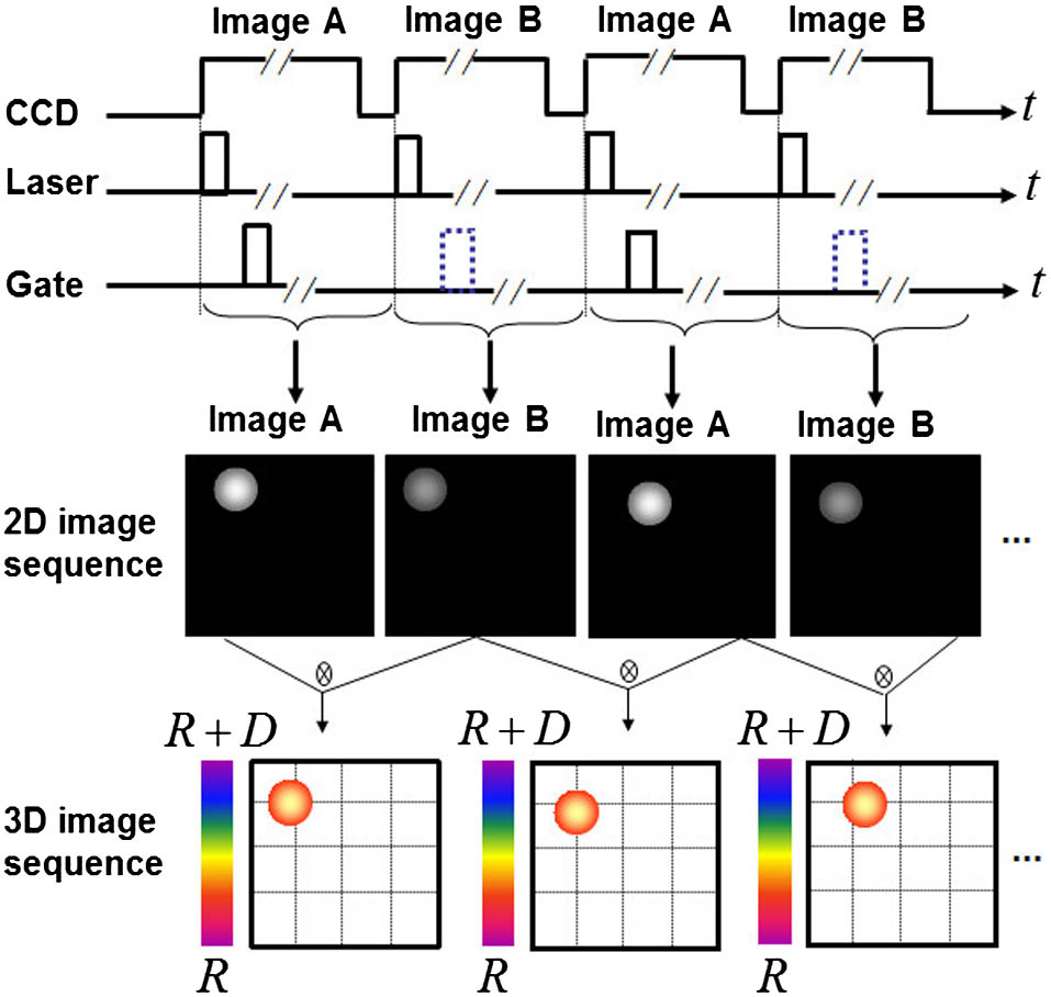
In 3DSRGI, each laser pulse triggers a camera with a highly sensitive gate, so that a number of laser pulses are integrated on a CCD and a CCD eventually produces a 2D gate image. As depicted in Fig. 1, to realize real-time 3DSRGI, sequences of time coding 2D images (ABAB…) are recorded by a synchronization timing of ABAB mode which is generated by a timing control unit (TCU) to synchronize the laser and the gate as well as the CCD. Under the ABAB synchronization timing sequence the corresponding time-coding images of targets are output and the two consequent frames inevitably contain a gate image A and a gate image B. So target 3D information can always be reconstructed by the current frame and the previous frame, and thus the range-gated imaging can output 3D images at video rates corresponding to the CCD[9,10].
Figure 1.Principle of the time-coding method in 3DSRGI.
When the time-coding 3DSRGI is being operated, the pulsed laser,gate, and camera are fed the frequency and duration time by the TCU. Before each new gate image, the gate is fed with the new delay time by the TCU automatically. During this period, the camera is closed and the emitted laser pulses are ignored. After a CCD image is output, the image is marked with image A or image B and the image frames are counted to make sure the previous image existed, thus 3D reconstruction can be done after the current frame and the previous frame are checked out. Laser and camera settings can be changed online by a computer that is convenient to operators. The operation flowchart of the time coding method is illustrated in Fig. 2.
Sign up for Chinese Optics Letters TOC. Get the latest issue of Chinese Optics Letters delivered right to you!Sign up now
Figure 2.Flow chart of the time-coding real-time 3DSRRGI.
The ABAB mode timing sequence is illustrated in Fig. 3, in which the delay or is triggered by the emission of the laser pulse, i.e., the gate is onset by the time the center of the pulse width laser pulse is emitted from the laser. The subscript numbers the pulses recorded by the gate image A or B, thus we can exploit the high frequency of the laser pulse by collecting a large number of pulses on a gate image. At the delay time or , the camera opens for exposure of the gate time. Thus, when the pulsed laser, gate, and CCD are electrically triggered by the ABAB synchronization timing generated by the TCU, the timecoding 2D images (ABAB…) are recorded.
The key requirement in time-coding 3DSRGI is that the relationship between the laser pulse width and the gate exposure time should be [7] or [15]. A pulsed laser with a 33 ns pulse width means the gate exposure time should be 33 or 66 ns. Higher time delay precision also means high system resolution[16]. So the ABAB synchronization timing generated by the TCU should have a high precision of the time delay and pulse width, and when the pulsed laser, gate, and CCD are electronically triggered by the ABAB synchronization timing, high precision of the time delay between the laser pulse and its corresponding gate exposure time and high precision duration time of the laser pulse and gate can be obtained. The preferred option used to generate the synchronization timing is FPGA for reliability, independence, and system integration reasons. However, the synchronous control precision is limited by the minimum 5 ns clock cycle of the FPGA and the 5 ns precision of the time delay and pulse width is achieved with currently available FPGAs[12–14]. As the laser pulse width is usually fixed, thus delay time and gate width variations shorter than the clock cycle cannot be achieved. For example, a 66 ns gate exposure time cannot be achieved when the clock cycle is 5 ns because the width control step is 5 ns, which can only obtain gate exposure time integer multiples of 5 ns. The phase-shift method described below is used to improve the synchronous control precision without resorting to very high clock frequencies of the FPGA.
At first, the external input clock is multiplied and phase shifted into (a positive integer) signals with the same frequency by a digital clock manager (DCM) of the FPGA. The zero phase-shifted signal is called FPGA’s global clock and the delay step between two adjacent signals is : that is, . These phase-shifted signals are processed to develop signals with a width (a positive integer) times the global clock and frequency of by a designed frequency and pulse module of FPGA, which mathematically can be described as where is the amplitude of the signals, and is the step signal that can be expressed as Then signal delayed (a positive integer) and (a positive integer) times the global clock, respectively, which can be given as When choosing one signal from and choosing another one from , then adding them up to develop the final output signal gives Equation (7) demonstrates the final output signal is delayed with a width of , where the delay and width precision are . By applying the phase-shift method, the precision of the time delay and width are improved to the level of of the global clock, which is equivalent to using a global clock to do the synchronization control. When the pulsed laser and gate are electronically triggered by the final output signal , the delay and gate width accuracy of the imaging system are improved to of the FPGA’s global clock cycle. What is more, because is a positive integer that can be set freely, the delay and width precision can meet a wide range of accuracy requirements in theory. The principle of the precision improvement of time delay and pulse width by the phase-shift method is shown in Fig. 4.
A TCU with a Spartan 6 FPGA is being designed to confirm the improvement of the-phase shift method and the results are presented in Table 1, Table 2, and Fig. 5. An external 50-MHz initial clock produced by the hardware is multiplied and phase shifted into 5 signals with the same frequency of 200 MHz by a DCM of the FPGA. The delay step between two adjacent signals of the 5 signals is 1 ns; that is, 0, 1, 2, 3, and 4 ns. The laser pulse is produced with a width of 50 ns, which is ten times that of the global clock. To test the delay precision improvement by the phase-shift method, and are designed with the parameters , , , 1, 2, 3, 4, , and . Referring to Eq. (8), the gate pulse was generated with a time duration of 50 ns and delayed 50, 51, 52, 53, and 54 ns with respect to the laser pulse. To test the pulse width precision improvement by the phase-shift method, and were designed with the parameters , , , , and , 1, 2, 3, 4. Referring to Eq. (8), the gate pulse wass generated with a time duration of 50, 51, 52, 53, and 54 ns. The experimental results were been measured by an oscilloscope with an error of 100 ps. In Fig. 5, the yellow one is the laser pulse and the red one is the gate pulse; the comparison of the theoretical values and experimental values of the time delay between the laser pulse and its corresponding gate pulse and the gate pulse width are shown in Tables 1 and 2, and the respective delay time of 54 ns and gate pulse width 51 ns oscilloscope test results are shown in Fig. 5.
Figure 5.Improvement of delay and width precision using the phase-shift method: (a) the delay time between the laser pulse and gate pulse is 54 ns; (b) the time duration of the gate pulse is 51.009 ns.
Table 1 illustrates that the delay time between the laser pulse and gate pulse can be changed with a step of 1 ns, approximately, which coincides with the theoretical results. In theory, the delay times between the laser pulse and the gate pulse are 50, 51, 52, 53, and 54 ns, but the experimental results are 52.9, 54, 55.2, 56.0, and 57.1 ns. Considering the measurement error caused by the oscilloscope and the 170.063 ns phase error which is stimulated by the ISE14.7 edition, we can conclude that the experimental results have an inherent delay of 3 ns respect to the theoretical results. The increased 3 ns can be explained by the signal layout path delay that takes a signal some time to transmit to the output port and can be solved by preset parameters. The result of 1 ns delay step is five times higher than the global clock cycle 5 ns referring to 200 MHz.
The results in Table 2 show that the experimental results of gate duration time were 49.707, 51.009, 51.550, 52.811, and 53.442 ns. The experimental data is incremented in line with the theoretical data 50, 51, 52, 53, and 54 ns. However, the difference of each experimental result and its corresponding theoretical results has no regularity. Analysis of this phenomenon can be summarized as the phase shift error and peak-to-peak jitter as well as the circuit of the signal output and the signal output interface. We can get that the 200 MHz phase shifted 5 signals have a maximum phase error of 170.053 ps, and the gate pulse was obtained by two transistor-transistor logical signals, and , superposition; both have 173.685 ps maximum peak-to-peak jitter by the ISE14.7 edition stimulation. Taking the measurement error caused by the oscilloscope into consideration, the maximum error would be 443.738 ps. What is more, the width of the pulse is also affected by the circuit of the signal output and the signal output interface, which is easily distracted by environmental factors. It is worth pointing out that, by the phase-shift method, we can achieve a pulse width precision close to 1 ns, which is less than the global clock cycle 5 ns referring to 200 MHz.
All of the above analysis confirms the improvement of the delay and width precision to 1 ns or close to 1 ns by the phase-shift method compared with 5 ns achieved by the conventional method[12–14].
To prove the ns-scaled time-coding method for 3DSRGI described in this Letter, a prototype measurement system was developed. A TCU designed by a microcontroller unit (MCU) and a FPGA is used to realize the communication between the imaging system and ABAB synchronization timing control. The system control and image processing software is designed in C++, the FPGA is written by Verilog, and the MCU is developed in C. The experiments were done with an outdoor imaging system consisting of a pulse laser wavelength of 808 nm with a 100 mW average power and a digital camera coupled to a GEN 2.5 intensifier on a night with all road lamps off. Two persons were separated by 5 m standing face to face along the road with a distance of 200 m from the nearer person to the imaging system. During the experiments, the system was driven with a pulsed laser and gated camera that is electronically driven by a TCU to emit laser pulses of 40 ns pulse width and control gate pulses of 40 ns duration time. The image A has a delay time of 1139 ns and the image B has a delay time of 1179 ns, respectively. A CCD sensor records an 8-bit gray-level image at a video rate of 10 Hz with a resolution of . Figures 6(a)–6(d) recorded a process of a person throwing a basketball, and Figs. 6(e)–6(h) reconstructed the process with a depth accuracy less than 0.5 m at 1 0 Hz. The experimental results illustrated in Fig. 6 demonstrate that the ns-scaled time-coding method for 3DSRGI can achieve real-time 3D imaging.
Figure 6.Real-time gate viewing images and super-resolution 3D reconstruction: (a)–(d) ns-scaled time coding 2D images; (e)–(h) super-resolution 3D reconstruction images.
In conclusion, we present analytical formulas and experimental proof of the ns-scaled time-coding method for 3DSRGI. By using the time-coding method, the active imaging system can achieve real-time 3D imaging in dynamic environments, and the phase-shift method we promoted was proved to increase the timing synchronization control precision to 1 ns with a single FPGA of 5 ns clock cycle. This work is beneficial to the improvement of the high-precision synchronous timing control and real-time working ability of range-gated imaging systems.