
Yuxi Wang, Zhaokun Wang, Xing Feng, Ming Zhao, Cheng Zeng, Guangqiang He, Zhenyu Yang, Yu Zheng, Jinsong Xia. Dielectric metalens-based Hartmann–Shack array for a high-efficiency optical multiparameter detection system[J]. Photonics Research, 2020, 8(4): 482
- Photonics Research
- Vol. 8, Issue 4, 482 (2020)
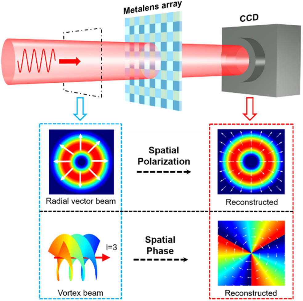
Fig. 1. Schematic shows the dielectric metalens-based Hartmann–Shack array for a high-efficiency optical multiparameter detection system. The system can simultaneously measure the spatial polarization and phase profiles of optical beams. The colors are only used to enhance the clarity of the image and to distinguish metalenses with different polarization sensitivities in the array.
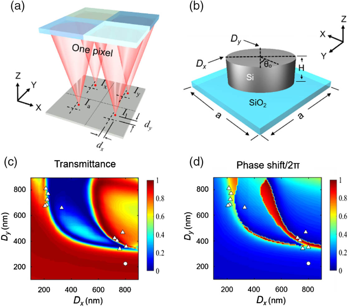
Fig. 2. Schematic and design of metalenses. (a) Scheme for one pixel of a metalens array. (The colors indicate different polarizations.) The dotted crosses on the focal plane correspond to the centers of particular metalenses. (b) Scheme for one unit element of a metalens; (c), (d) simulation results for intensity transmittance and phase shifts of unit elements under normal incidence of y x y D x = 800 nm , D y = 224 nm l
Fig. 3. Scanning electron micrographs and intensity distributions of a manufactured metalens array. (a) Local scanning electron micrograph of a fabricated metalens array. The white rectangle indicates one pixel of the array. (b) Corresponding magnified scanning electron micrograph of one pixel, where the polarization bases are denoted by letters for each metalens; (c)–(d) oblique view of the selected parts of the metalenses; (e)–(f) intensity profiles along the x y l
Fig. 4. Experimental validation of SOP detection with one pixel. (a) Optical setup for polarization detection. LP, linear polarization; λ / 4 λ / 2 20 × x y a b l r S 1 S 2 S 3 Data File 1 ).
Fig. 5. Detection and reconstruction of two vector beams. (a), (b) Intensity distributions for two vector beams. The blue arrows denote the local SOPs. (c), (d) Raw data of measured focal points for two vector beams; (e), (f) reconstructed polarization profiles. The black arrows correspond to the measured local polarization vectors, and the red arrows correspond to the theoretical predictions. The dashed gray lines are drawn to identify individual pixels.
Fig. 6. Detection and reconstruction of the vortex beam. (a) Schematic of the optical setup. L1, L2, L3, L4, lens; A, aperture; P, polarizer; SP, splitter prism; SLM, spatial light modulator; and OL, objective lens. (b) Intensity distribution for the vortex beam; (c) raw data of measured focal points for the vortex beam; (d) phase gradients (pink arrows denote theoretical results, and black arrows denote experimental results) and reconstructed wavefront (false-color scale) of the vortex beam. The dashed lines are drawn in above images to distinguish individual pixels of the metalens array. The length of the reference arrow is 0.4 rad/μm.

Set citation alerts for the article
Please enter your email address
© Copyright 2018-2021 | Chinese Laser Press. All Rights Reserved 沪ICP备15018463号-20