
Yang Li, Chao Liang, Gaopeng Wang, Jielei Li, Shi Chen, Shihe Yang, Guichuan Xing, Hui Pan. Two-step solvent post-treatment on PTAA for highly efficient and stable inverted perovskite solar cells[J]. Photonics Research, 2020, 8(10): A39
- Photonics Research
- Vol. 8, Issue 10, A39 (2020)
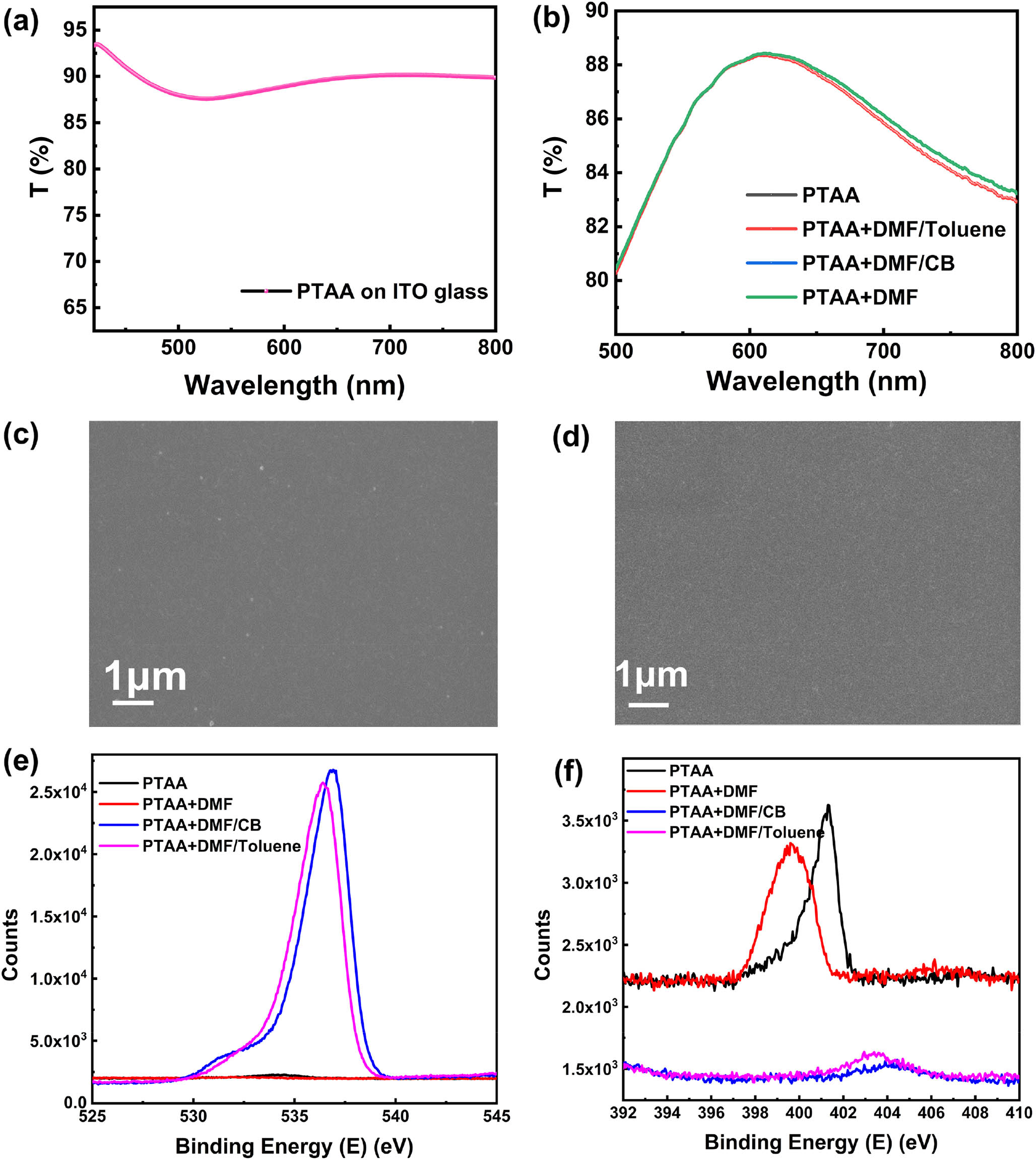
Fig. 1. Transmittance of PTAA on (a) ITO glass and on (b) electronic grade pure glass; SEM (scale bar = 1 μm
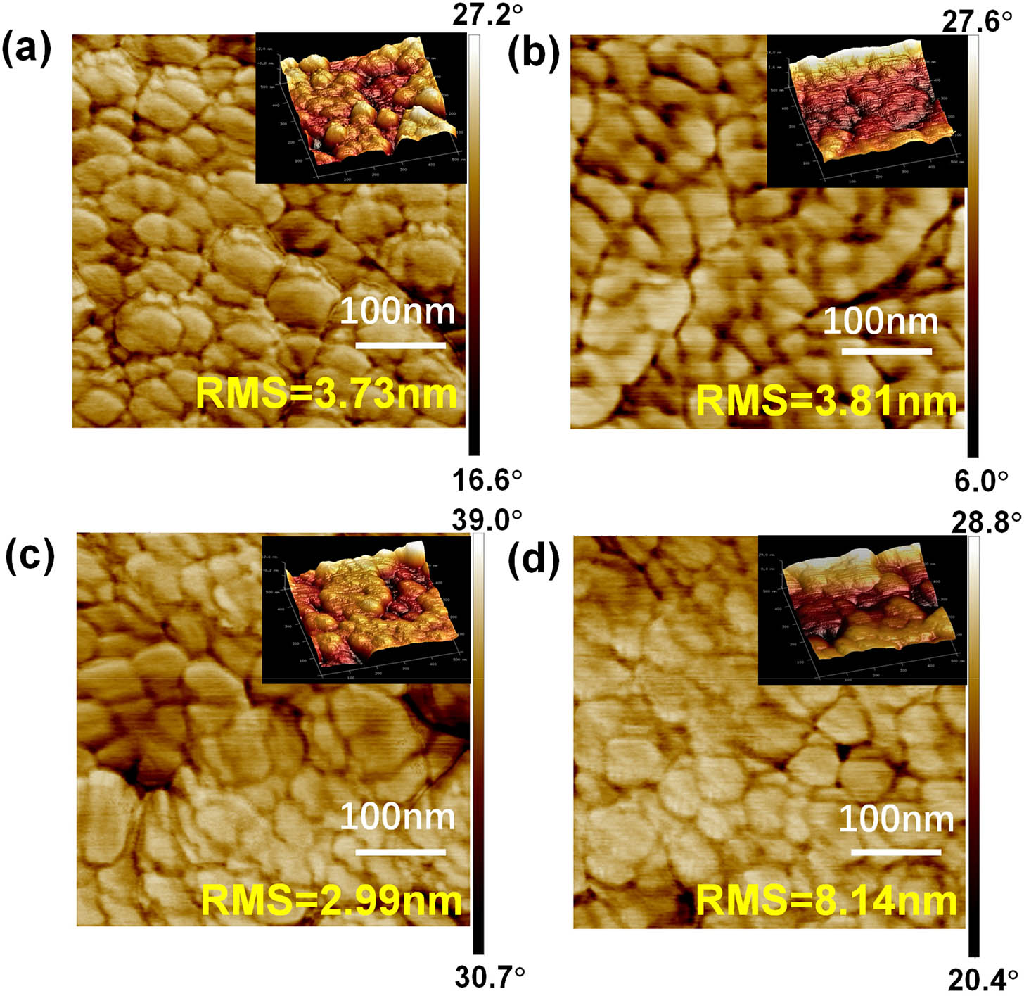
Fig. 2. AFM phase images (500 nm × 500 nm
Fig. 3. (a)–(c) Cross-sectional SEM images for devices with PTAA, PTAA/DMF/CB, and PTAA/DMF/toluene as HTLs, respectively. (d)–(h) Top-view SEM images of perovskite film on glass/PTAA, glass, glass/PTAA/DMF/toluene, glass/PTAA/DMF, and glass/PTAA/DMF/CB. (Red circles show pin holes.) (i)–(l) Contact angles for (i) PTAA; (j) PTAA/DMF; (k) PTAA/DMF/CB, and (l) PTAA+DMF/toluene on glass.
Fig. 4. Top-view AFM images (1 μm × 1 μm
Fig. 5. (a) XRD patterns and (b) UV-vis absorption spectra for PTAA/PSK, PTAA/DMF/PSK, PTAA/DMF/CB/PSK, and PTAA/DMF/toluene/PSK on ITO substrates. (c) Steady-state PL and (d) TRPL spectra for PSCs corresponding to the films in (a) and (b).
Fig. 6. (a) J-V curve under 1.5G sunlight through a solar simulator by reverse scan for PSCs using PTAA with different concentrations (device structure: ITO/PTAA/PSK/PCBM/BCP/Ag). (b) Best device based on toluene-treated PTAA. (c) to (g) J-V curves for devices based on different PTAA substrates by reverse and forward scans: (d) PTAA without any treatment; (e) PTAA treated with DMF; (f) PTAA treated with DMF/CB. The active area for the above cells is 0.05 cm 2
Fig. 7. (a) Device structure. (b) Enlarged drawing of toluene between PTAA and perovskite. (c) Energy-level diagram of each layer in the device. (d) Fabrication process of PSCs based on DMF/toluene-treated PTAA. (e) J-V curves (by reverse scan) for the devices in this research. (f) Nyquist plot for PSCs with pristine PTAA and PTAA treated by DMF, DMF/CB, and DMF/toluene, respectively (bias voltage = 0.6 V
Fig. 8. Data difference analysis for 36 PSCs by using toluene-treated PTAA as hole transport material in inverted structure.
Fig. 9. Photovoltaic parameters of the best device (with DMF/toluene modified PTAA as HTL) newly prepared as well as after storage in N 2 J sc V oc
|
Table 1. Film Thickness Measurement Result by a Step Profiler
|
Table 2. Contact Angle Measurement Results Corresponding to PTAA with Different Solvent Treatmenta
|
Table 3. TRPL Time Decay Analysis Through Double Exponential Fitting Method
|
Table 4. Long-Term Stability for Devices with Pristine PTAA Compared with PTAA Treated by DMF, DMF/Toluene, and DMF/CB, with Different Storage Times
| |||||||||||||||||||||||||||||||||||||||||
Table 5. Photovoltaic Parameters of the Best Solar Cell with Toluene-Treated PTAA as HTL at Different Storage Times (Measured 21 Times, 30 s Once Under Continuous 1.5G Sunlight Without Encapsulation)

Set citation alerts for the article
Please enter your email address
© Copyright 2018-2021 | Chinese Laser Press. All Rights Reserved 沪ICP备15018463号-20