Abstract
Modifying the surface of poly[bis(4-phenyl)(2,4,6-trimethylphenyl)amine] (PTAA) with toluene during the high-speed spin-coating process of dimethylformamide considerably improves the wettability and morphology of PTAA and results in improvement of the crystallinity and absorption of perovskite film. The hole mobility and ohm contact have also been improved accordingly. Combined with these improved parameters, inverted perovskite solar cells with high efficiency of 19.13% and long-term stability could be achieved, which are much better than those with untreated PTAA. Importantly, our devices can keep 88.4% of the initial power conversion efficiency after 30 days of storage in ambient air.
1. INTRODUCTION
Organic–inorganic hybrid metal-halide perovskites have been considered as leading materials in solar-energy harvesting for their long carrier diffusion length, strong light absorption, and suitable bandgap [1]. Impressively, the efficiency of perovskite solar cells (PSCs) improved dramatically from 3% to 25.2% within 10 years [2,3]. However, their long-term stability remains a bottleneck for commercial application [4,5]. In order to improve their efficiency and stability simultaneously, various techniques have been developed recently [6,7]. For example, morphology engineering through self-assembled monolayers (SAMs) has been developed as an effective way to achieve this target [8]. Recently, researchers have also fabricated highly efficient PSCs by surface modification of poly(3-hexylthiophene) film with a certified efficiency of 22.7% [9]. It is believed that adjusting the film thickness with post-treatment of the hole transport layer (HTL) is a good way for fabricating highly efficient PSCs [10].
The structures of planar PSCs nowadays mainly include two types, i.e., n-i-p (conventional structure) and p-i-n (inverted structure) [11]. Particularly, the inverted PSCs show higher stability than conventional PSCs because they avoid using synonyms, i.e., -Tetrakis[N, N-di(4-methoxyphenyl)amino]--spirobifluorene (Spiro-MeOTAD), which is sensitive to water [12]. Importantly, the HTL plays a critical role in the high efficiency of inverted PSCs [13]. Various HTLs, such as poly[bis(4-phenyl)(4-butylphenyl)amine](Poly-TPD) [14], CuSCN [15], CuO [16], poly(3,4-ethylenedioxythiophene)-poly(styrenesulfonate) (PEDOT:PSS) [17], and , have been widely investigated. Among them, PTAA-based PSCs have received great attention in recent years. The PTAA doped with [(2,3,5,6-tetrafluoro-2,5-cyclohexadiene-1,4-diylidene)dimalononitrile,7,7,8,8-tetracyano-2,3,5,6-tetrafluoroquinodimethane] (F4-TCNQ) or -tris[phenyl (m-tolyl)amino]triphenylamine was first used as HTL in p-i-n devices by Prof. Huang, which showed an efficiency of up to 18.3% [18,19]. Recently, Zhu et al. reported that the inverted PSCs with the same HTL achieved an efficiency of up to 21% through a simple solution-processed secondary growth technique [20]. In 2017, n-i-p PSCs based on PTAA recorded maximum efficiency of 22.1% through iodide management [21], surpassing the normal tyrant, -tetrakis[N,N-di(4-methoxyphenyl)amino]--spirobifluorene (Spiro-MeOTAD) at one point. Additionally, PTAA can also be used in conventional PSCs for improving stability due to its hydrophobic properties [22]. However, the intrinsic hydrophobic property of PTAA makes the perovskite precursor difficult to spread out on its surface. Since PTAA is smooth and does not wet DMF and DMSO, the perovskite precursor is hardly spun on top of it. Many scientists have tried interfacial engineering via surface modification to increase the surface activity of PTAA toward perovskites to solve this problem [23,24]. However, these methods need a large amount of perovskite precursors to cover the surface of PTAA, which aggrandizes the cost of PSCs, thus hindering the commercialization of PSCs.
Herein, we report, for the first time to our knowledge, a novel strategy to fabricate efficient and stable inverted PSCs with pure PTAA (without any dopant) as an HTL by two-step solvent post-treatment and thickness control of PTAA film in an all-solution and low-temperature process. It shows that the efficiency of our device with toluene-treated PTAA can be up to 19.13%, which is better than 17.2% for the untreated sample. Interestingly, our device without any encapsulation shows high stability with an efficiency of 94.5% after 20 days in ambient air and 88.4% after 30 days. The enhanced efficiency and improved stability are attributed to (1) the greatly enhanced hydrophilicity and improvement of PTAA by surface modification through toluene and DMF and (2) the improved ohm contact, reduced impedance, and enhanced crystallinity of perovskite film due to the post-treatment of PTAA and its adjusting film thickness. Our findings demonstrate that the surface modification of HTL by the solvent is an effective way to fabricate PSCs with long-term stability and high efficiency simultaneously. In particular, our method is not only easy to be realized under mild conditions [such as all-solution process, low temperature, and concentration of 40 ppm (parts per million) in the glove box during fabrication], but it also reduces the amount of perovskite precursor, which may be useful for large-scale fabrication of inverted flexible PSCs with reduced cost in the future.
Sign up for Photonics Research TOC. Get the latest issue of Photonics Research delivered right to you!Sign up now
2. EXPERIMENT
A. Materials
2, 9-dimethyl-4,7-diphenyl-1,10-phenanthroline (BCP, ), formamidinium iodide (FAI, ), methyl ammonium bromide (MABr, ), lead bromide (, ), PTAA (, ), and Phenyl C61 butyric acid methyl-ester synonym () were all bought from Xi’an Polymer Light Technology Corp. Silver (, commercial), chlorobenzene (CB, , Acros), dimethylformamide (DMF, , Sigma), dimethyl sulfoxide (DMSO, , Acros), and toluene (, Sigma) are all kept in a -filled glovebox before use. The pre-patterned indium tin oxide (ITO) glasses were bought from South China Xiang Science & Technology Company Limited.
B. Device Fabrication
At first, ITO glasses were cleaned by an ultrasonic washer with deionized water, alcohol, acetone, and IPA in succession for 15 min. The as-cleaned ITO substrates were treated with oxygen plasma for 15 min and were then delivered into a -filled glovebox. The as-prepared PTAA solution 2.5 mg/mL in CB was spin-coated onto the ITO glasses in two steps: 500 rpm for 5 s (with a ramping speed of 500 rpm/s) and 4500 rpm for 30 s (with a ramping speed of 1000 rpm/s). Then, the samples were annealed on a hotplate at 105°C for 10 min and then cooled down to 25°C (room temperature, RT). The as-prepared PTAA films were divided into three groups. In order to increase the wettability of PTAA, we spin-coated 150 μL DMF on PTAA at 4000 rpm for 30 s as Group A. For Group B and Group C, we dropped 40 μL CB and 40 μL toluene onto the center of the substrates at 20 s during the DMF spin-coating process (ramping speed of 4000 rpm/s), respectively. We also tried dropping CB or toluene after the DMF washing process (under steady state) for further comparison.
The perovskite precursor was prepared by mixing 1336.93 mg , 475.08 mg FAI, 54.58 mg MABr, and 178.93 mg in a 2.5 mL mixed solvent (volume ratio ) and then stirred at 70°C for 1 h. The as-prepared perovskite precursor was filtered with a 0.45 μm PTFE filter prior to use and then spin-coated onto the above three PTAA layers in a two-step program: at 2000 rpm for 10 s (with a ramping speed of 500 rpm/s) and then at 6000 rpm for 35 s (with a ramping speed of 2000 rpm/s). During the second step, we dropped 150 μL CB onto the center of the substrates at around 20 s. The perovskite film annealed on a hotplate at 105°C for 90 min and then cooled down to room temperature. The electron transport layer (20 mg/mL in CB) was spin-coated onto the perovskite layer at the speed of 1200 rpm for 40 s (with a ramping speed of 400 rpm/s) and left to dry in petri dishes for 15 min. Then, all samples were spin-coated by 120 μL BCP (0.5 mg/mL in IPA) at 4500 rpm for 35 s (with a ramping rate of 1000 rpm/s).
Afterward, 100 nm silver was thermally evaporated in a vacuum chamber () as the electrodes: the evaporation speed was around 0.1 Å/s (1 Å = 0.1 nm) in the first 20 nm, then increased to 0.5 Å/s in the middle 40 nm, and at last reached 1 angstrom/s for the last 40 nm. The active area of the cells was defined by the overlap of the ITO and the Ag () for each by using a metal shadow mask. The above process was completed in a -filled glovebox with oxygen and humidity both lower than 10 ppm, and the atmosphere and temperature change will influence the results.
C. Materials Characterization
The ultraviolet-visible (UV-vis) absorption spectra of the perovskite films and the transmittance of PTAA films were recorded by UV-2600 (Shimazu), and the scanning electron microscope (SEM) images were obtained by Zeiss Sigma. Atomic force microscope (AFM) images were measured by Bruker FastScan, and the root mean square of Ra (RMS) for all films was measured. X-ray diffraction (XRD) measurement was conducted through a Rigaku (RINT-2500) X-ray diffractometer (Cu radiation, ). A drop shape analyzer (OSA100S-T-P) recorded the contact angles of PTAA, and a step profiler (DEKTAK-XT) measured the thickness of perovskite. The photoluminescence (PL) was recorded through Acton SpectraPro SP-2500 (Princeton Instrument), and time-resolved photoluminescence (TRPL) was measured by a universal streak camera C10910 series under dark in ambient air at room temperature. (The excitation source is a femtosecond laser with 400 nm wavelength, 100 fs pulse width, and 1 kHz repetition rate. The excitation energy density is set to be with spot diameter of 4 mm.) X-ray photoelectron spectroscopy (XPS) measurement was conducted by a Therno scientific XPS system (ESCALAB Xi+).
D. Solar Cell Measurement
J-V (current density versus voltage) curve was measured through a Keithley 2400 source meter, and a 425 W collimated xenon lamp was used as the light source. The scan range is from 0 to 1.3 V, and 100 points were recorded with 30 ms dwell time for each; further, there is no pre-illumination for all J-V measurements. The light intensity is calibrated through a solar simulator (Newport) to (AM 1.5G). The incident photon-to-electron conversion efficiency (IPCE) was measured by a Zolix IPCE measurement system (SCS10-X150A-DSSC-CB07) in alternating current (AC) mode. The electrochemical impedance spectroscopy (EIS) measurement was completed with a Solartron electrochemical workstation (the frequency range is 0.1–1 Hz, and the bias voltage is 0.6 V). All devices were kept in ambient conditions with humidity around 35%, and the above measurements were performed under RT.
3. RESULTS AND DISCUSSION
As important parameters for the efficiency of a solar cell, the transmittance and morphology of PTAA were characterized at first. The transmittance of PTAA through ITO glass is as high as 90% in the visible light range [Figs. 1(a) and 1(b)], indicating that ITO/PTAA has good light transmission. SEM images show that the surface of PTAA on ITO is much smoother and more compact than on pure glass [Figs. 1(c) and 1(d)], which may lead to improved ohm contact and is beneficial for holes to be easily extracted from a perovskite (PSK) layer.
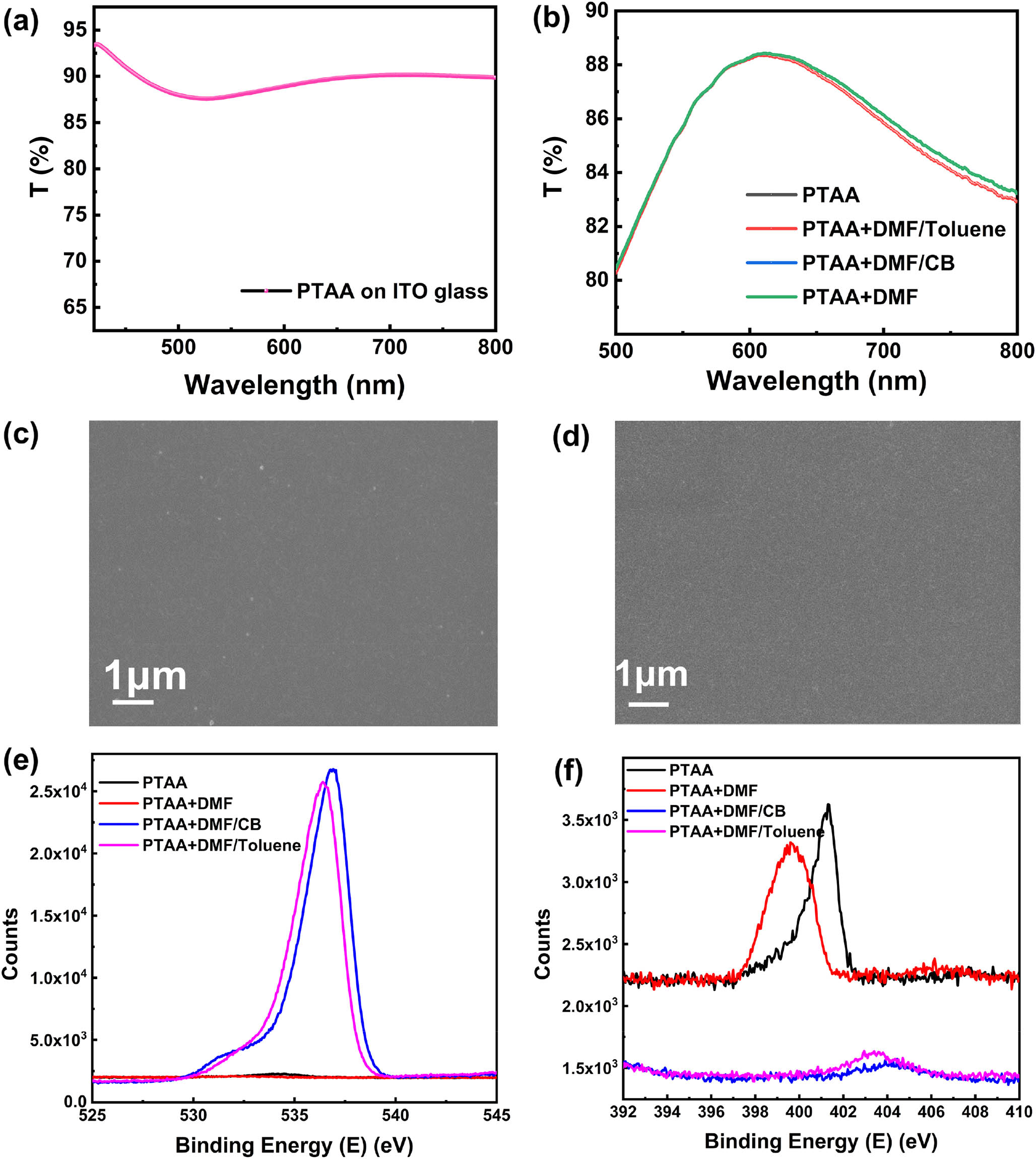
Figure 1.Transmittance of PTAA on (a) ITO glass and on (b) electronic grade pure glass; SEM () images of (c) ITO glass and (d) PTAA precursor covered ITO glass. XPS profiles for PTAA, PTAA+DMF, PTAA+DMF/CB, and PTAA+DMF/toluene on ITO substrate: (e) scan for O 1s; (f) scan for N 1s.
In order to improve the wettability of PTAA (perovskite is hydrophilic), a small amount of CB or toluene, was dropped onto the PTAA layer during the spin-coating process of DMF. Interestingly, through this method, the perovskite precursor can be easily spread out on the treated PTAA surface. We then measured the thickness of PTAA (2.5 mg/mL in CB), which is around 15 nm. In order to study the thickness change of PTAA, we then conducted XPS measurement for the four PTAA layers with different treatments. XPS results confirmed high amounts of oxygen with a simultaneous decrease in nitrogen upon CB or toluene treatment of PTAA. This is in line with a decrease in the thickness of PTAA [reduced N, Fig. 1(e)], while consequently more ITO [an increase in O, Fig. 1(f)] was visible from the surface. Both CB and toluene could erode PTAA film to some extent during the process of spin coating DMF under high speed; however, the relatively high polarity of CB molecules resulted in its better ability to dissolve PTAA. The whole methodology is two-step solvent post-treatment of PTAA. CB could easily dissolve PTAA, leading to more dissolved PTAA loss, while toluene showed less erosion. Additionally, AFM images (Fig. 2) showed that the PTAA film was eroded seriously by CB, which caused the uneven surface of CB-treated PTAA. While for MB-treated PTAA, the film was not seriously eroded, the surface quality of PTAA was improved after the toluene treatment, and PTAA appeared smooth with lower unevenness.

Figure 2.AFM phase images () of (a) ITO/PTAA, (b) ITO/PTAA/DMF, (c) ITO/PTAA/DMF/toluene, and (d) ITO+PTAA/DMF/CB. (Insets show the 3D morphology for each film and RMS reflects the film roughness.)
Considering the above better PTAA film quality, we tried to fabricate inverted devices based on PTAA, i.e., PTAA treated with CB or toluene to find their difference. In order to gain further insight, SEM measurements were conducted after device fabrication, as shown in Fig. 3. The erosion of the PTAA surface was later found for the CB-treated PTAA film, which was proved either from cross-sectional SEM images [Fig. 3(a)–3(c)] or thickness measurements (Table 1). Both the perovskite film and PTAA layer become much flatter after the toluene treatment [Figs. 3(c)–3(e)], confirming that our methodology can effectively improve the morphology of PTAA and crystallinity of perovskite. However, the PTAA film treated by toluene becomes thinner compared with the film coated by DMF; it confirmed the heavy erosion caused by toluene. In contrast, the surface of CB-treated PTAA became uneven due to the high dissolution of PTAA into CB or the erosion of CB to PTAA [Fig. 3(d)], which is consistent with the aforementioned AFM results. In the top-view SEM images [Fig. 3(d)–3(h)], perovskite film on PTAA appears flat and has fewer pinholes, compared with perovskite on ITO glass. A washing with DMF can effectively suppress traps; however, it cannot prevent the formation of pinholes on perovskite [Fig. 3(g)]. Interestingly, when we used the PTAA treated with toluene or CB during DMF washing, the pinholes on perovskite almost disappeared. Besides, the perovskite film on PTAA treated by toluene also had larger grain size compared with that by CB [Figs. 3(f) and 3(h)], indicating the crystallinity of the former was higher. [Note: thickness measurements for the four films by a step profiler (Table 1) also confirmed these observations.] Moreover, the contact angle was measured to study the surface difference of PTAA after treatment [Figs. 3(i)–3(l) and Table 2]. The contact angle became small for the toluene-treated PTAA due to improved hydrophilicity. Compared with PTAA without treatment, the film is easier for perovskite to spread on. Improvement in the wettability of the PTAA layer is a key factor for the perovskite to form a film with high quality. Experimentally, the contact angle change was different for CB- and toluene-treated PTAAs. For CB, it dissolved PTAA aggressively, leading to direct contact with glass in some parts with a contact angle around 60 deg, which may destroy the solar cells. However, there is no such problem for toluene. It can be concluded that CB can reduce the thickness more aggressively compared with toluene. The thickness change in PTAA film will have a huge influence on device performance. More erosion will have a negative effect on the efficiency and stability of a solar cell. Besides, AFM results showed that PTAA/DMF/toluene/PSK offered the best morphology and the lowest RMS (only 5.77 nm) among all considered perovskites (Fig. 4). From the above discussion, we concluded that the toluene modification of PTAA improved the surface morphology and provided the perovskite with better crystallinity, which is beneficial for holes transportation and enhances ohm contact.
Figure 3.(a)–(c) Cross-sectional SEM images for devices with PTAA, PTAA/DMF/CB, and PTAA/DMF/toluene as HTLs, respectively. (d)–(h) Top-view SEM images of perovskite film on glass/PTAA, glass, glass/PTAA/DMF/toluene, glass/PTAA/DMF, and glass/PTAA/DMF/CB. (Red circles show pin holes.) (i)–(l) Contact angles for (i) PTAA; (j) PTAA/DMF; (k) PTAA/DMF/CB, and (l) PTAA+DMF/toluene on glass.
| Group | PTAA+DMF+CB+PSK | PTAA+DMF+toluene+PSK | PTAA+DMF+PSK | PTAA |
| Thickness | 450 nm | 456 nm | 459 nm | 15 nm |
Table 1. Film Thickness Measurement Result by a Step Profiler
| Group | θ(M) | θ(L) | θ(R) |
| PTAA | 107.30 | 106.49 | 108.10 |
| PTAA/DMF | 106.80 | 106.68 | 106.92 |
| PTAA/CB | 60.48 | 60.91 | 60.04 |
| PTAA/toluene | 81.94 | 84.06 | 79.80 |
Table 2. Contact Angle Measurement Results Corresponding to PTAA with Different Solvent Treatmenta
Figure 4.Top-view AFM images () of perovskites on PTAA with different solvent modification during (rotating state) or after spin coating of DMF (stable state): (a) glass/PTAA/DMF/toluene (drop under stable state)+PSK; (b) glass/PTAA/PSK; (c) glass/PTAA/DMF/toluene (drop while rotating)/PSK; (d) glass/PTAA/DMF/PSK; (e) glass+PTAA/DMF/CB (drop while rotating)/PSK; (f) glass+PTAA/DMF/CB (drop under stable state)/PSK.
In order to further investigate the effect of solvent treatment of PTAA on perovskite, XRD was carried for the samples: (1) ITO/PTAA/PSK, (2) ITO/PTAA/DMF/PSK, (3) ITO/PTAA/DMF/CB/PSK, and (4) ITO/PTAA/DMF/toluene/PSK. By removing the XRD signals of ITO and glass in Fig. 5(a), we can clearly see that Sample (4) has the highest crystallinity with sharp characteristic peaks of crystal [25,26]. Besides, the characteristic peaks of at in all samples are relatively weak, especially in Sample (4), ITO/PTAA/DMF/toluene/PSK, indicating its highest quality of perovskite. Sample (2), ITO/PTAA/DMF/CB/PSK, also has better crystallinity of perovskite than other samples but lower than Sample (4). A small excess of is beneficial for increasing the grain size of perovskites, which can promote the crystallization of perovskite film [27,28]. However, a high excess of will influence the purity of perovskite, resulting in low crystallinity and degradation [29]. From the characterizations above, we conclude that our solvent engineering strategy of PTAA by either toluene or CB is beneficial for improving the crystallization of perovskite film, and, among them, toluene is better.
Figure 5.(a) XRD patterns and (b) UV-vis absorption spectra for PTAA/PSK, PTAA/DMF/PSK, PTAA/DMF/CB/PSK, and PTAA/DMF/toluene/PSK on ITO substrates. (c) Steady-state PL and (d) TRPL spectra for PSCs corresponding to the films in (a) and (b).
In order to study the optical properties of the above perovskite layers on ITO glasses, we then analyzed the UV-vis spectra. As shown in Fig. 5(b), ITO/PTAA/DMF/toluene/PSK film shows the strongest light absorption after 550 nm. We think the enhanced crystallization of perovskite film and improved morphology of PTAA film caused by surface modification contributed greatly to the above enhancement.
In order to further understand the carrier dynamics inside PTAA, we measured the PL and TRPL for the considered samples. The PSK film treated by toluene during DMF spin-coating had the lowest PL emission intensity at 765 nm among all groups, indicating that holes can be more effectively extracted by constructed PTAA through toluene treatment [Fig. 5(c)]. The toluene-treated PTAA film can effectively promote the charge separation and avoid the recombination of carriers in perovskite compared with untreated PTAA films. Moreover, the charge quenching procedure [Fig. 5(d)] is in accordance with the PL result. The PL lifetime of carriers in PTAA/DMF/toluene layer is the shortest among all samples (Table 3). Compared with other films, the perovskite based on toluene-treated PTAA (during the DMF spin-coating) showed the shortest quenching time, indicating that most holes are extracted from the perovskite to PTAA with little charge recombination. The average PL lifetime of PTAA/DMF/toluene/PSK film was 1.88 ns, which was much shorter than that of PTAA/PSK (6.50 ns). Due to the reduced thickness of PTAA, the PL lifetime of CB-treated PTAA was the second shortest, and PL emission intensity was the second weakest among all samples. However, because of the strong erosion of perovskite, the transport ability of holes was still worse than that of PTAA/DMF/toluene/PSK. The TRPL curves were double exponentially fitted, and the average PL decay time was calculated according to similar methods employed by other researchers [30]. The double exponential fitting function of PL decay used in this research is
| Group | A1 | A2 | τ1(ns) | τ2(ns) | τaverage(ns) |
| PTAA/DMF/CB/PSKa | 126.65 | 1.96 | 1.82 | 7.41 | 2.15 |
| PTAA/DMF/toluene/PSKa | 211.51 | 2.66 | 1.72 | 5.66 | 1.88 |
| PTAA/DMF/PSK | 10.03 | 0.94 | 3.48 | 11.40 | 5.35 |
| PTAA/DMF/toluene/PSKb | 236.25 | 1.99 | 1.56 | 8.69 | 1.88 |
| PTAA/DMF/CB/PSKb | 26.54 | 1.56 | 2.61 | 7.72 | 3.37 |
| PTAA/PSK | 16.95 | 0.86 | 2.72 | 17.86 | 6.50 |
Table 3. TRPL Time Decay Analysis Through Double Exponential Fitting Method
Here, is the decay time and is the weight factor of each decay channel.
The average PL lifetime is calculated from the and values of the above fitted curve data with the following Eq. (2): Values of and for our experiments are shown in Table 3.
According to Table 3 and Fig. 5(d), the holes extraction ability of PTAA/DMF/toluene (drop while rotating) is the strongest, with both first decay time () and second decay time () sharply decreased, compared with other films. In the double exponential fitting decay for the perovskite film, stands for the monomolecular recombination time, while reflects the time for recombination of holes and electrons [31,32]. The smaller , the shorter time for holes to be extracted from the perovskite to the anode, indicating that the HTL can transfer carriers and reduce recombination of charges efficiently [33]. The shortest for PTAA/DMF/toluene (drop while rotating)+PSK demonstrates its best ability for hole transportation among all measured layers. Meanwhile, the shortest means that the perovskite based on toluene-treated PTAA has the least recombination of holes and electrons, where toluene molecules build up a pathway for holes more effectively to be transported, reduce the ohm contact, and improve the mobility of carriers. The improved carrier transportation and separation of hole–electron pairs will enhance performance of the solar device.
It is speculated that the toluene molecules may connect perovskites and PTAA, like a bridge, forming a much tighter contact with each other and contributing to the transportation process of holes.
Optimizing the thickness of HTL is crucial for fabricating highly efficient inverted PSCs because thicker PTAA can guarantee higher fill factor of PSCs, while thinner PTAA will enhance the current density due to the reduced series resistance. In this work, we tried different PTAA concentrations (10, 5, and 2.5 mg/mL) before using surface-modified PTAA as HTL for fabricating PSCs with the structure of and found that the performance of the device with 2.5 mg/mL PTAA was the best [Fig. 6(a)]. We finally fabricated PSCs based on the same device structure by replacing PTAA (2.5 mg/mL) with DMF, DMF/CB, and DMF/toluene-treated ones and compared them with the pristine device to investigate the effects of interface engineering on the device performance. J-V curves for the above devices are shown in Fig. 6. The champion device based on toluene-treated PTAA showed an efficiency of 19% and of [Fig. 6(b)]. At different scan modes, the hysteresis of all PSCs was very small [Fig. 6(c)–6(f)], indicating that all the cells were current stable. Compared with the conventional structure, the inverted devices have less hysteresis due to more balanced electron and hole fluxes and reduced surface traps [34].
Figure 6.(a) J-V curve under 1.5G sunlight through a solar simulator by reverse scan for PSCs using PTAA with different concentrations (device structure: ITO/PTAA/PSK/PCBM/BCP/Ag). (b) Best device based on toluene-treated PTAA. (c) to (g) J-V curves for devices based on different PTAA substrates by reverse and forward scans: (d) PTAA without any treatment; (e) PTAA treated with DMF; (f) PTAA treated with DMF/CB. The active area for the above cells is .
The device structure, bandgap relationship, and detailed device fabrication process are shown in Figs. 7(a)–Fig. 7(d), respectively. Figure 7(e), together with Fig. 6, shows that the PSCs with toluene-treated PTAA has the highest efficiency among all devices due to the improved short-circuit current density (), fill factor (FF), and open-circuit voltage (). The IPCE for the previously mentioned PSCs was then measured just after the fabrication. Figure 7(g) reveals that the external quantum efficiency (EQE) of PSCs shows a consistent result. The integrated current density () calculated from IPCE for the best device was slightly less than the current density in the J-V curve [ in Fig. 6(f)] due to the change of measurement condition and storage delay. In order to find the reason of efficiency enhancement, we also performed EIS measurement for the devices under a bias voltage of 0.6 V. The radius of the semicircle in the Nyquist plot for the device based on PTAA/DMF/toluene was much smaller than that of the other devices, reflecting its reduced resistance [35] [Fig. 7(f)], which is caused by the high surface quality of PTAA, enhanced crystallinity of perovskite, and an improved ohm contact. Therefore, we conclude that the interface engineering, PTAA modified with toluene, can dramatically improve performance of the solar cell by reducing impedance and surface traps. Moreover, a series of PSCs based on PTAA modified by DMF/toluene was fabricated. The data difference analysis of the 36 cells fabricated using toluene-treated PTAA showed that most of the devices have efficiency above 17%, near 1.08 V, fill factor (FF) in the range of 65% to 71%, and around (Fig. 8), which is much higher than that of the other devices, confirming that our fabrication process is repeatable and our result is reliable.
Figure 7.(a) Device structure. (b) Enlarged drawing of toluene between PTAA and perovskite. (c) Energy-level diagram of each layer in the device. (d) Fabrication process of PSCs based on DMF/toluene-treated PTAA. (e) J-V curves (by reverse scan) for the devices in this research. (f) Nyquist plot for PSCs with pristine PTAA and PTAA treated by DMF, DMF/CB, and DMF/toluene, respectively (, frequency in range of 0.1–100 Hz). (g) IPCE curves of PSCs by using PTAA, PTAA/DMF, PTAA/DMF/CB, and PTAA/DMF/toluene as HTLs. (h) Long-term stability test for PSCs fabricated based on PTAA treated by different solvents in ambient with humidity above 35% and temperature around RT.
Figure 8.Data difference analysis for 36 PSCs by using toluene-treated PTAA as hole transport material in inverted structure.
Last but not least, we carried out the long-term stability test for our best devices based on PTAA/DMF, PTAA/DMF/toluene, and PTAA/DMF/CB without any treatment. The J-V measurement lasted for 30 days in ambient air and at RT; further, all measured devices were used without any encapsulation and photopathic operation. The device with PTAA treated by DMF/toluene retained 94.5% efficiency after 20 days and 88.4% after 30 days [Fig. 7(h) and Table 4], which is much higher than that of the other devices, indicating that the PSCs fabricated by DMF/toluene modified PTAA have higher stability. Moreover, the photovoltaic parameters for the best device with PTAA/DMF/toluene under continuous 1.5G illumination were obtained at different storage stages: freshly made, after 20 days, and after 30 days. The efficiency-exposure time relationships were almost linear during the period for the devices based on toluene-treated PTAA at different stages (Fig. 9), further demonstrating that the device under the light irradiation is quite stable. Compared with the fresh cell, even after 20-day storage in ambient conditions, the device with toluene-treated PTAA as HTL showed only 16.8% loss in average efficiency, 6.8% loss in average open circuit voltage (), and 11% loss in average short current density (). Interestingly, the average FF increased from 78.0% to 78.9% during the process (Table 5) possibly due to the improved crystallinity and interfacial contact during storage [36]. (Note: after storage in ambient conditions for 20 days, the average efficiency dropped from 18.95% to 15.75%, the average from 1.02 to 0.95 V, and the average from 23.44 to , measured with continuous exposure to 1.5G sunlight for 650 s.) The hydrophobicity of PTAA contributed greatly to the device stability, where the perovskite active layer was protected by a sandwich-like structure with an up-layer of PCBM and a down-layer of PTAA.
| Storage Time | | | Efficiency (%) | |
| PTAA | PTAA/DMF | PTAA/DMF/toluene | PTAA/DMF/CB |
| 24 h | 17.20 | 16.86 | 19.31 | 18.78 |
| 240 h | 16.84 | 15.95 | 18.78 | 17.88 |
| 480 h | 13.29 | 15.65 | 18.24 | 16.37 |
| 720 h | 4.79 | 7.05 | 17.07 | 15.00 |
Table 4. Long-Term Stability for Devices with Pristine PTAA Compared with PTAA Treated by DMF, DMF/Toluene, and DMF/CB, with Different Storage Times
Figure 9.Photovoltaic parameters of the best device (with DMF/toluene modified PTAA as HTL) newly prepared as well as after storage in -filled glove box for 10 and 20 days (measured under continuous 1.5G light illumination, 30 s once, in ambient). Relationships between exposure time and exposure time and (a) efficiency, (b) , (c) , and (d) FF, respectively.
| Parameters | Fresh Cells | 10 Days Later | 20 Days Later |
| FF | Average | 78.00 | 78.60 | 78.94 |
| Maximum | 80.11 | 81.64 | 80.65 |
| Jsc (mA/cm2) | Average | 23.44 | 21.95 | 20.87 |
| Maximum | 23.87 | 23.63 | 22.72 |
| Efficiency (%) | Average | 18.95 | 17.00 | 15.75 |
| Maximum | 19.51 | 17.68 | 16.17 |
| Voc (V) | Average | 1.02 | 1.00 | 0.96 |
| Maximum | 1.09 | 1.10 | 0.98 |
Table 5. Photovoltaic Parameters of the Best Solar Cell with Toluene-Treated PTAA as HTL at Different Storage Times (Measured 21 Times, 30 s Once Under Continuous 1.5G Sunlight Without Encapsulation)
4. CONCLUSION
In summary, we presented a novel strategy, i.e., two-step post-solvent treatment of PTAA, to improve the efficiency and stability of inverted PSCs. We found that modifying the surface of PTAA by toluene during the DMF washing process shows enhanced hydrophilicity, best optimized film thickness, and improved morphology of PTAA, which resulted in highly improved crystallinity and absorption of perovskite film on treated PTAA. Accordingly, we showed that the devices demonstrated enhanced ohm contact and hole transport ability. Finally, we further established an efficiency above 19% and a high stability with retaining 88.4% of its initial efficiency kept even after 30 days of storage in ambient air (humidity around 30%, without photopathic operation). The devices also have excellent reproducibility and little hysteresis. Additionally, our methodology can reduce the usage of perovskite precursor, which may be recommended as an effective way for fabricating PSCs on a large scale, especially for flexible PSCs under mild conditions. Our findings provide an insightful strategy to improve the efficiency and stability of PSCs by simple interface engineering and will have practical applications in industries.
Acknowledgment
Acknowledgment. The authors acknowledge financial support from the above funding and appreciate technician J. Xu’s help on SEM measurement. Also great thanks to Prof. S. Yang for measurement of IPCE.
References
[1] M. A. Green, A. Ho-Baillie, H. J. Snaith. The emergence of perovskite solar cells. Nat. Photonics, 8, 506-514(2014).
[2] A. Kojima, K. Teshima, Y. Shirai, T. Miyasaka. Organometal halide perovskites as visible-light sensitizers for photovoltaic cells. J. Am. Chem. Soc., 131, 6050-6051(2009).
[3] National Renewable. Best-research-cell-efficiencies-20200406.
[4] J. A. Christians, S. N. Habisreutinger, J. J. Berry, J. M. Luther. Stability in perovskite photovoltaics: a paradigm for newfangled technologies. ACS Energy Lett., 3, 2136-2143(2018).
[5] H. J. Jung, D. Kim, S. Kim, J. Park, V. P. Dravid, B. Shin. Stability of halide perovskite solar cell devices: in situ observation of oxygen diffusion under biasing. Adv. Mater., 30, 1802769(2018).
[6] A. Rajagopal, K. Yao, A. K. Y. Jen. Toward perovskite solar cell commercialization: a perspective and research roadmap based on interfacial engineering. Adv. Mater., 30, 1800455(2018).
[7] L. F. Liu, A. Y. Mei, T. F. Liu, P. Jiang, Y. S. Sheng, L. J. Zhang, H. W. Han. Fully printable mesoscopic perovskite solar cells with organic silane self-assembled monolayer. J. Am. Chem. Soc., 137, 1790-1793(2015).
[8] L. J. Zuo, Z. W. Gu, T. Ye, W. F. Fu, G. Wu, H. Y. Li, H. Z. Chen. Enhanced photovoltaic performance of CH3NH3PbI3 perovskite solar cells through interfacial engineering using self-assembling monolayer. J. Am. Chem. Soc., 137, 2674-2679(2015).
[9] E. H. Jung, N. J. Jeon, E. Y. Park, C. S. Moon, T. J. Shin, T.-Y. Yang, J. H. Noh, J. Seo. Efficient, stable and scalable perovskite solar cells using poly(3-hexylthiophene). Nature, 567, 511-515(2019).
[10] Y. Li, L. Ji, R. Liu, C. Zhang, C. H. Mak, X. Zou, H.-H. Shen, S.-Y. Leu, H.-Y. Hsu. A review on morphology engineering for highly efficient and stable hybrid perovskite solar cells. J. Mater. Chem. A, 6, 12842-12875(2018).
[11] S. I. Seok, M. Gratzel, N. G. Park. Methodologies toward highly efficient perovskite solar cells. Small, 14, 1704177(2018).
[12] T. Liu, K. Chen, Q. Hu, R. Zhu, Q. Gong. Inverted perovskite solar cells: progresses and perspectives. Adv. Energy Mater., 6, 1600457(2016).
[13] S. Ameen, M. A. Rub, S. A. Kosa, K. A. Alamry, M. S. Akhtar, H. S. Shin, H. K. Seo, A. M. Asiri, M. K. Nazeeruddin. Perovskite solar cells: influence of hole transporting materials on power conversion efficiency. ChemSusChem, 9, 10-27(2016).
[14] X. W. Xu, C. Q. Ma, Y. H. Cheng, Y. M. Xie, X. P. Yi, B. Gautam, S. M. Chen, H. W. Li, C. S. Lee, F. So, S. W. Tsang. Ultraviolet-ozone surface modification for non-wetting hole transport materials based inverted planar perovskite solar cells with efficiency exceeding 18%. J. Power Sources, 360, 157-165(2017).
[15] N. Arora, M. I. Dar, A. Hinderhofer, N. Pellet, F. Schreiber, S. M. Zakeeruddin, M. Gratzel. Perovskite solar cells with CuSCN hole extraction layers yield stabilized efficiencies greater than 20%. Science, 358, 768-771(2017).
[16] C. T. Zuo, L. M. Ding. Solution-processed Cu2O and CuO as hole transport materials for efficient perovskite solar cells. Small, 11, 5528-5532(2015).
[17] J. B. You, Z. R. Hong, Y. Yang, Q. Chen, M. Cai, T. B. Song, C. C. Chen, S. R. Lu, Y. S. Liu, H. P. Zhou, Y. Yang. Low-temperature solution-processed perovskite solar cells with high efficiency and flexibility. ACS Nano, 8, 1674-1680(2014).
[18] Q. Wang, C. Bi, J. Huang. Doped hole transport layer for efficiency enhancement in planar heterojunction organolead trihalide perovskite solar cells. Nano Energy, 15, 275-280(2015).
[19] C. Bi, Q. Wang, Y. Shao, Y. Yuan, Z. Xiao, J. Huang. Non-wetting surface-driven high-aspect-ratio crystalline grain growth for efficient hybrid perovskite solar cells. Nat. Commun., 6, 7747(2015).
[20] D. Y. Luo, W. Q. Yang, Z. P. Wang, A. Sadhanala, Q. Hu, R. Su, R. Shivanna, G. F. Trindade, J. F. Watts, Z. J. Xu, T. H. Liu, K. Chen, F. J. Ye, P. Wu, L. C. Zhao, J. Wu, Y. G. Tu, Y. F. Zhang, X. Y. Yang, W. Zhang, R. H. Friend, Q. H. Gong, H. J. Snaith, R. Zhu. Enhanced photovoltage for inverted planar heterojunction perovskite solar cells. Science, 360, 1442-1446(2018).
[21] W. S. Yang, B. W. Park, E. H. Jung, N. J. Jeon, Y. C. Kim, U. L. Dong, S. S. Shin, J. Seo, E. K. Kim, J. H. Noh. Iodide management in formamidinium-lead-halide-based perovskite layers for efficient solar cells. Science, 356, 1376-1379(2017).
[22] Y. Shao, Y. Yuan, J. Huang. Correlation of energy disorder and open-circuit voltage in hybrid perovskite solar cell. Nat. Energy, 1, 15001(2016).
[23] J. Cao, B. H. Wu, R. H. Chen, Y. Y. Q. Wu, Y. Hui, B. W. Mao, N. F. Zheng. Efficient, hysteresis-free, and stable perovskite solar cells with ZnO as electron-transport layer: effect of surface passivation. Adv. Mater., 30, 1705596(2018).
[24] T. Singh, S. Oz, A. Sasinska, R. Frohnhoven, S. Mathur, T. Miyasaka. Sulfate-assisted interfacial engineering for high yield and efficiency of triple cation perovskite solar cells with alkali-doped TiO2 electron-transporting layers. Adv. Funct. Mater., 28, 1706287(2018).
[25] Y. Reyna, M. Salado, S. Kazim, A. Pérez-Tomas, S. Ahmad, M. Lira-Cantu. Performance and stability of mixed FAPbI3(0.85)MAPbBr3(0.15) halide perovskite solar cells under outdoor conditions and the effect of low light irradiation. Nano Energy, 30, 570-579(2016).
[26] K. T. Cho, S. Paek, G. Grancini, C. Roldán-Carmona, P. Gao, Y. Lee, M. K. Nazeeruddin. Highly efficient perovskite solar cells with a compositionally engineered perovskite/hole transporting material interface. Energy Environ. Sci., 10, 621-627(2017).
[27] Y. C. Kim, N. J. Jeon, J. H. Noh, W. S. Yang, J. Seo, J. S. Yun, A. Ho-Baillie, S. J. Huang, M. A. Green, J. Seidel, T. K. Ahn, S. Seok. Beneficial effects of PbI2 incorporated in organo-lead halide perovskite solar cells. Adv. Energy Mater., 6, 1502104(2016).
[28] T. J. Jacobsson, J.-P. Correa-Baena, E. H. Anaraki, B. Philippe, S. D. Stranks, M. E. F. Bouduban, W. Tress, K. Schenk, J. Teuscher, J.-E. Moser, H. Rensmo, A. Hagfeldt. Unreacted PbI2 as a double-edged sword for enhancing the performance of perovskite solar cells. J. Am. Chem. Soc., 138, 10331-10343(2016).
[29] V. Ramana, H. Su, Y. Wu, H. Wu, J. Xie, X. Liu, J. Fan, J. Dai, Z. He. Photon-generated carriers excited superoxide species inducing long-term photoluminescence enhancement of MAPbI3 perovskite single crystals. J. Mater. Chem. A, 5, 12048-12053(2017).
[30] W. Chen, G.-N. Zhang, L. Xu, R. Gu, Z. Xu, H. Wang, Z. He. Low temperature processed, high-performance and stable NiOx based inverted planar perovskite solar cells via a poly(2-ethyl-2-oxazoline) nanodots cathode electron-extraction layer. Mater. Today Energy, 1, 1-10(2016).
[31] H. Zhang, J. Cheng, F. Lin, H. He, J. Mao, K. S. Wong, A. K. Jen, W. C. Choy. Pinhole-free and surface-nanostructured NiOx film by room-temperature solution process for high-performance flexible perovskite solar cells with good stability and reproducibility. ACS Nano, 10, 1503-1511(2016).
[32] A. Abrusci, S. D. Stranks, P. Docampo, H. L. Yip, A. K. Jen, H. J. Snaith. High-performance perovskite-polymer hybrid solar cells via electronic coupling with fullerene monolayers. Nano Lett., 13, 3124-3128(2013).
[33] Q. Dong, Y. Fang, Y. Shao, P. Mulligan, J. Qiu, L. Cao, J. Huang. Electron-hole diffusion lengths > 175 μm in solution-grown CH3NH3PbI3 single crystals. Science, 347, 967-970(2015).
[34] J. H. Heo, H. J. Han, D. Kim, T. K. Ahn, S. H. Im. Hysteresis-less inverted CH3NH3PbI3 planar perovskite hybrid solar cells with 18.1% power conversion efficiency. Energy Environ. Sci., 8, 1602-1608(2015).
[35] M. Bag, L. A. Renna, R. Y. Adhikari, S. Karak, F. Liu, P. M. Lahti, T. P. Russell, M. T. Tuominen, D. Venkataraman. Kinetics of ion transport in perovskite active layers and its implications for active layer stability. J. Am. Chem. Soc., 137, 13130-13137(2015).
[36] J. A. Bartelt, D. Lam, T. M. Burke, S. M. Sweetnam, M. D. McGehee. Charge-carrier mobility requirements for bulk heterojunction solar cells with high fill factor and external quantum efficiency >90%. Adv. Energy Mater., 5, 1500577(2015).


