• Photonics Research
  • Vol. 11, Issue 10, 1757 (2023)
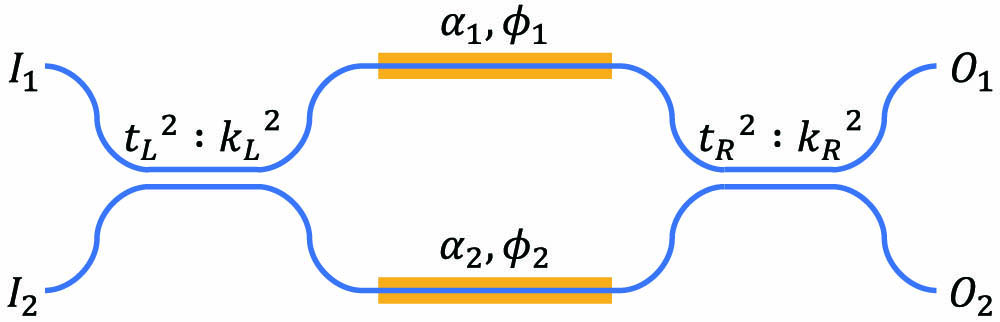
Peng Bao1, Qixiang Cheng1,*, Jinlong Wei2,3, Giuseppe Talli2..., Maxim Kuschnerov2 and Richard V. Penty1|Show fewer author(s)
Author Affiliations
  • 1Centre for Photonic Systems, Electrical Engineering Division, Department of Engineering, University of Cambridge, Cambridge CB3 0FA, UK
  • 2Huawei Technologies Duesseldolf GmbH, European Research Center, 80992 Munich, Gemany
  • 3Current address: Peng Cheng Laboratory, Shenzhen 518000, China
  • show less
    DOI: 10.1364/PRJ.492807 Cite this Article Set citation alerts
    Peng Bao, Qixiang Cheng, Jinlong Wei, Giuseppe Talli, Maxim Kuschnerov, Richard V. Penty, "Harnessing self-heating effect for ultralow-crosstalk electro-optic Mach–Zehnder switches," Photonics Res. 11, 1757 (2023) Copy Citation Text show less
    Schematic of a 2 × 2 switch cell.
    Fig. 1. Schematic of a 2×2 switch cell.
    Cross-section schematic of the differential E-O phase shifter pair.
    Fig. 2. Cross-section schematic of the differential E-O phase shifter pair.
    (a) Insertion loss for the E-O phase shifter with varying lightly doped region widths (0–2 μm) plotted against absolute phase shift for different device lengths. (b) and (c) Insertion loss and phase shift for 50-μm- and 1000-μm-long E-O phase shifters against bias voltage. Both phase shifters share a common lightly doped region width of 2 µm. (d) and (e) Insertion loss for the E-O phase shifter with a 50 μm length and 2 μm lightly doped region width, plotted against absolute phase shift for different doping concentrations. (f) Insertion loss for the E-O phase shifter with a 1000 μm length and no lightly doped region, plotted against phase shift for different doping concentrations. Note that the dark curves in (d)–(f) represent the projection of the original 3D curves onto the loss–bias plane.
    Fig. 3. (a) Insertion loss for the E-O phase shifter with varying lightly doped region widths (0–2 μm) plotted against absolute phase shift for different device lengths. (b) and (c) Insertion loss and phase shift for 50-μm- and 1000-μm-long E-O phase shifters against bias voltage. Both phase shifters share a common lightly doped region width of 2 µm. (d) and (e) Insertion loss for the E-O phase shifter with a 50 μm length and 2 μm lightly doped region width, plotted against absolute phase shift for different doping concentrations. (f) Insertion loss for the E-O phase shifter with a 1000 μm length and no lightly doped region, plotted against phase shift for different doping concentrations. Note that the dark curves in (d)–(f) represent the projection of the original 3D curves onto the loss–bias plane.
    (a) Insertion loss of E-O phase shifters plotted against the provided phase shift, with the yellow dashed line representing PS2 at 30 μm length. (b) Insertion loss of the differential E-O phase shifter pair plotted against the provided phase shift, featuring a red dashed line for PS2 at the 30 μm length. (c) Current in the two E-O phase shifters plotted against the applied bias voltage.
    Fig. 4. (a) Insertion loss of E-O phase shifters plotted against the provided phase shift, with the yellow dashed line representing PS2 at 30 μm length. (b) Insertion loss of the differential E-O phase shifter pair plotted against the provided phase shift, featuring a red dashed line for PS2 at the 30 μm length. (c) Current in the two E-O phase shifters plotted against the applied bias voltage.
    (a) τrise for PS2 under pulse excitation technique with varying overdrive voltages. Inset shows a close-up of τrise for bias voltage over 3 V. (b) Control scheme for reducing τrise: bias voltage applied to PS2 (top) and corresponding waveguide core temperature change (bottom); shadowed region indicates 90%–100% of steady-state temperature. (c) Temperature distribution for PS2 at 20 ns (left) and 20 μs (right) after an excitation pulse followed by a step signal. Insets illustrate waveguide core temperature. (d) Control scheme for reducing τfall: bias voltage applied to PS2 and PS1 (top), corresponding waveguide core temperature change (middle), and resulting phase shift (bottom); shadowed region indicates 0%–10% of steady-state phase difference between the two phase shifters.
    Fig. 5. (a) τrise for PS2 under pulse excitation technique with varying overdrive voltages. Inset shows a close-up of τrise for bias voltage over 3 V. (b) Control scheme for reducing τrise: bias voltage applied to PS2 (top) and corresponding waveguide core temperature change (bottom); shadowed region indicates 90%–100% of steady-state temperature. (c) Temperature distribution for PS2 at 20 ns (left) and 20 μs (right) after an excitation pulse followed by a step signal. Insets illustrate waveguide core temperature. (d) Control scheme for reducing τfall: bias voltage applied to PS2 and PS1 (top), corresponding waveguide core temperature change (middle), and resulting phase shift (bottom); shadowed region indicates 0%–10% of steady-state phase difference between the two phase shifters.
    (a) Schematic of the CTDC. (b) Wavelength response for the CTDC under different width variation values. (d) Cross-coupling ratio at 1.55 μm versus the power dissipated for the CTDC.
    Fig. 6. (a) Schematic of the CTDC. (b) Wavelength response for the CTDC under different width variation values. (d) Cross-coupling ratio at 1.55 μm versus the power dissipated for the CTDC.
    (a)–(c) Schematics of the three configurations. (d)–(f) Transmission spectra for each configuration in the cross and bar states under different width variations.
    Fig. 7. (a)–(c) Schematics of the three configurations. (d)–(f) Transmission spectra for each configuration in the cross and bar states under different width variations.
    Distribution of crosstalk ratio at 1.55 μm (left) and bandwidth at crosstalk of −30 dB (right) for the three configurations in cross (top) and bar (bottom) states across 400 trials assuming uniformly distributed fabrication variations. Note that the crosstalk ratio for the two-CTDC case is not visible on the left due to its complete suppression at 1.55 μm.
    Fig. 8. Distribution of crosstalk ratio at 1.55 μm (left) and bandwidth at crosstalk of 30  dB (right) for the three configurations in cross (top) and bar (bottom) states across 400 trials assuming uniformly distributed fabrication variations. Note that the crosstalk ratio for the two-CTDC case is not visible on the left due to its complete suppression at 1.55 μm.
    (a) Overall power penalty histograms for PILOSS (top) and DLN (bottom) switches at different scales, featuring breakdowns of (b) insertion loss and (c) crosstalk-induced power penalty.
    Fig. 9. (a) Overall power penalty histograms for PILOSS (top) and DLN (bottom) switches at different scales, featuring breakdowns of (b) insertion loss and (c) crosstalk-induced power penalty.
    Reference3 dB SplitterLoss (dB)Crosstalk (dB)/Bandwidth (nm)Switching Time (ns)Power (mW)DescriptionSchematic
    [22]MMI1 at 1.55 μma3.220.9E-O MZS (single-ended)
    [23]DC1.2426E-O MZS (push-pull)
    [24]MMI8N.A.40.8E-O DMZS
    [16]DC2434E-O NMZS
    [17]DC0.65bb at 1.55 μmaN.A.N.A.E-O BNMZS
    [18]DC1.2699E-O SDMZS
    [25]Y-splitter3 at 1.5 μma506T-O MZS (strip waveguide)
    [26]Y-splitter1.9 at 1.55 μma3620.7T-O MZS (MMI-PS)
    This workCurved DC2018Differential PS pair
    This workCurved DC & CTDC2023Differential PS pair + one CTDC
    This workCTDC2028Differential PS pair + two CTDCs
    Table 1. Example Elementary Silicon MZI Cells by Direct Carrier Injection
    ComponentLoss (dB)Crosstalk
    Si waveguide1.5 per cmN.A.
    90° bend0.014aN.A.
    Waveguide crossing0.05 [22]–40 [45]
    Transition waveguide0.02aN.A.
    Curved DC0.01aN.A.
    Regular E-O phase shifter0.7aN.A.
    Differential E-O phase shifter pair0 (cross)/2 (bar)aN.A.
    Edge coupler to fiber1.5 [46]N.A.
    Table 2. Loss and Crosstalk for Key Building Blocks
    Peng Bao, Qixiang Cheng, Jinlong Wei, Giuseppe Talli, Maxim Kuschnerov, Richard V. Penty, "Harnessing self-heating effect for ultralow-crosstalk electro-optic Mach–Zehnder switches," Photonics Res. 11, 1757 (2023)
    Download Citation