Na Han, Ting Ji, Yanxia Cui, Guohui Li, Hengkang Zhang, Yuying Hao. Research Progress of Two-Dimensional Layered Perovskite Materials and Their Applications[J]. Laser & Optoelectronics Progress, 2019, 56(7): 070002
Search by keywords or author
- Laser & Optoelectronics Progress
- Vol. 56, Issue 7, 070002 (2019)
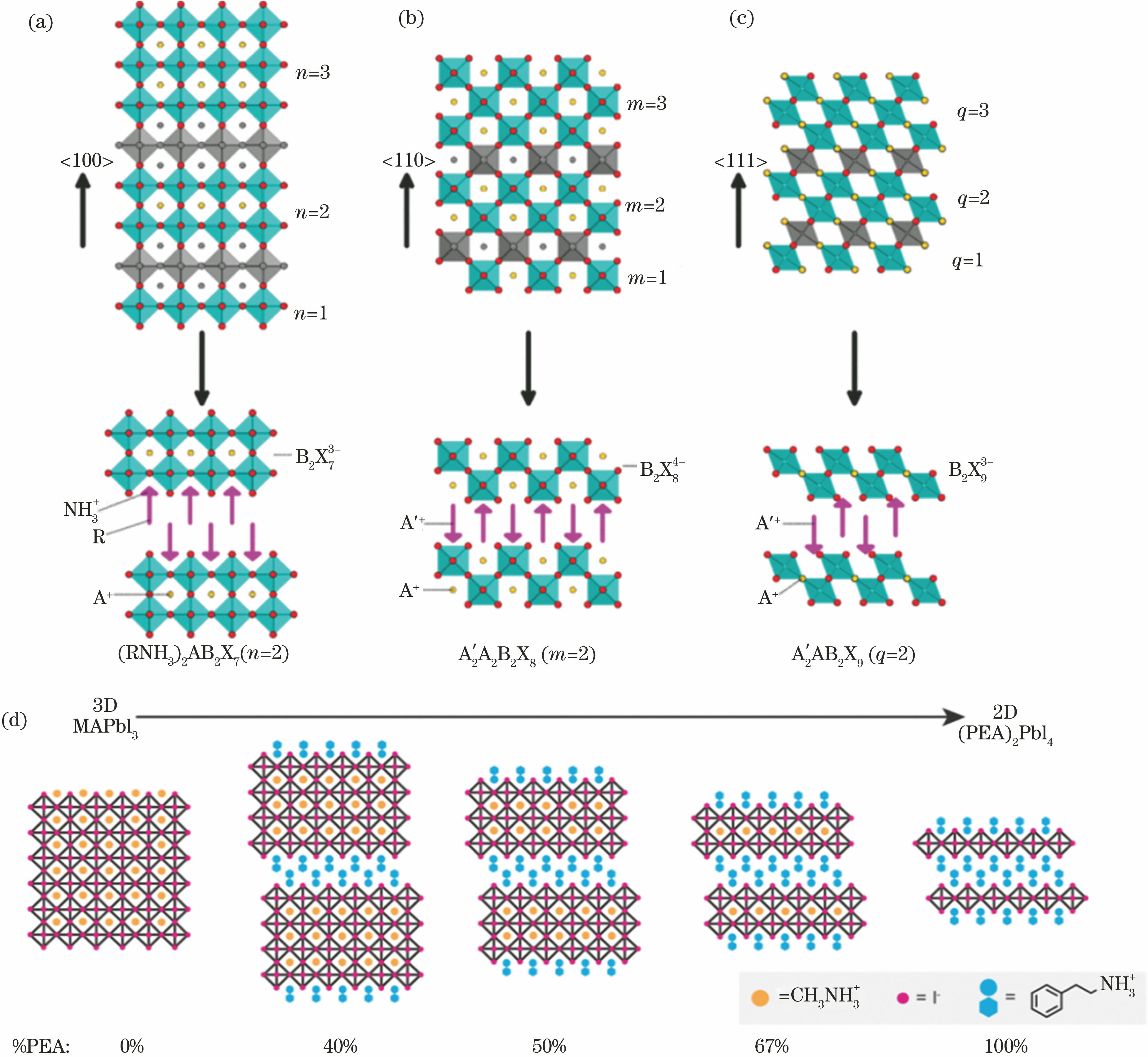
![Schematic of a two-dimensional perovskite structure cut from different directions of three-dimensional perovskites. (a) orientation; (b) orientation; (c) orientation [31]; (d) crystal structure diagram of MAPbI3, (PEA)2PbI4 and mixed MA-PEA two-dimensional perovskite materials[32]](/richHtml/lop/2019/56/7/070002/img_1.jpg)
Fig. 1. Schematic of a two-dimensional perovskite structure cut from different directions of three-dimensional perovskites. (a) <100> orientation; (b) <110> orientation; (c) <111> orientation [31]; (d) crystal structure diagram of MAPbI3, (PEA)2PbI4 and mixed MA-PEA two-dimensional perovskite materials[32]
![Structure, binding energy and band gap of two-dimensional perovskite. (a) Quasi-2D perovskite crystal structures[33]; (b) exciton binding energy (Eb) and band gap (Eg) in various 3D and two-dimensional perovskites[34]; (c) bandgap under different n values[48]](/richHtml/lop/2019/56/7/070002/img_2.jpg)
Fig. 2. Structure, binding energy and band gap of two-dimensional perovskite. (a) Quasi-2D perovskite crystal structures[33]; (b) exciton binding energy (Eb) and band gap (Eg) in various 3D and two-dimensional perovskites[34]; (c) bandgap under different n values[48]
Fig. 3. Schematic of structure and performance of the solar cells. (a) Cross-sectional SEM image and J-V curves of devices with (PEA)2(MA)2Pb3I10 as absorber layer; (b) PXRD patterns of perovskite films[63]; (c) current densities as a function of time[48]; (d) J-V curves for devices with (BA)2(MA)3Pb4I13 as absorbing layer, inset showing the device architecture[67]; (e) J-V curves for devices under different conditions [69]; (f) J-V curve for devices at a peak efficiency of Cs5-2D perovskite solar cell
Fig. 4. Schematic of structure and performance of LEDs. (a) Structure of EL device[88]; (b) chromaticity coordinates of illuminants. Inset showing the emission spectra[90]; (c) luminescence of LEDs device[92]; (d) structure of quasi-2D perovskite LEDs[50]; (e) dependence of current density and luminance on driving voltage for the device [94]; (f) EQE versus voltage of the devices[95]; (g) EQE of the best devices with passivation layer; (h) current efficiency-voltage curves of devices [97]
Fig. 5. Schematic of structure and performance of photodetector. (a) Structure diagram of Au/HTL/CHPI/mp-TiO2/c-TiO2 /FTO photodetector; (b) corresponding EQE spectra of device[101]; (c) schematic of (BA)2(MA)n-1PbnI3n+1 photodetector; (d) linear relationship between photocurrent and incident light intensities of photodetectors[102]; (e) schematic illustration of photodetector with interdigital graphene electrodes; (f) current-voltage curves of device[103]; (g) photoresponses of photodetector; (h) enlar

Set citation alerts for the article
Please enter your email address


