Abstract
A brief review of Huang–Rhys theory and Albrechtos theory is provided, and their connection and applications are discussed. The former is a first order perturbative theory on optical transitions intended for applications such as absorption and emission involving localized defect or impurity centers, emphasizing lattice relaxation or mixing of vibrational states due to electron–phonon coupling. The coupling strength is described by the Huang–Rhys factor. The latter theory is a second order perturbative theory on optical transitions intended for Raman scattering, and can in-principle include electron–phonon coupling in both electronic states and vibrational states. These two theories can potentially be connected through the common effect of lattice relaxation – non-orthonormal vibrational states associated with different electronic states. Because of this perceived connection, the latter theory is often used to explain resonant Raman scattering of LO phonons in bulk semiconductors and further used to describe the size dependence of electron–phonon coupling or Huang–Rhys factor in semiconductor nanostructures. Specifically, the A term in Albrechtos theory is often invoked to describe the multi-LO-phonon resonant Raman peaks in both bulk and nanostructured semiconductors in the literature, due to the misconception that a free-exciton could have a strong lattice relaxation. Without lattice relaxation, the A term will give rise to Rayleigh or elastic scattering. Lattice relaxation is only significant for highly localized defect or impurity states, and should be practically zero for either single particle states or free exciton states in a bulk semiconductor or for confined states in a semiconductor nanostructure that is not extremely small.1. Introduction
Electron–phonon coupling manifests in many ways in optical properties, and thus in optical spectroscopy studies of semiconductors. Two commonly observed phenomena, (1) phonon side bands or replicas in luminescence or absorption spectra, and (2) multiple orders of longitudinal optical (LO) phonon Raman lines, are both related to electron–phonon coupling. The first phenomenon may occur in radiative recombination associated with either defect or impurity, which was the primary subject of Huang and Rhys’ 1950 paper[1], or band edge states in an intrinsic semiconductor[2]. The second phenomenon is intrinsic in nature[2, 3], but sensitive to the presence of defects or impurities[2]. Here we will use intrinsic to mean a semiconductor free of defects and impurities. Although these phenomena might appear similar, their mechanisms can be rather different. This brief review intends to explain the differences in terms of underlying physics and to clarify some confusion in the literature.
Huang–Rhys factor S was initially introduced to describe the electron–phonon coupling strength of a localized (defect) center because of lattice relaxation, where lattice relaxation refers to the change in equilibrium atomic positions between the initial and final state involved in the optical transition[1]. For a defect center, the atomic configuration near the defect can change substantially between the ground state and an excited state[4]. However, between two bulk states, one of the conduction band and the other of the valence band, lattice relaxation should be minimal, if any. Because the wave functions of both states are extended, lattice relaxation would indicate one sublattice displacing against another, and thus causing a change in the lattice constant. Thus, one would not expect that exciting a few electrons into the conduction band would induce a change in interatomic bonding in a bulk semiconductor. Therefore, we do not expect the specific lattice relaxation effect described in Huang–Rhys theory to manifest itself in the optical transitions involving only bulk states.
This brief review will discuss two important topics of electron–phonon coupling that are highly relevant to optical spectroscopy studies of semiconductor materials and related nanostructures: (1) the difference between two primary approaches to treat the electron–phonon coupling, and their respective applications; and (2) the relationship between the Huang–Rhys theory[1] and Albrecht's theory for Raman scattering[5], including the inappropriate though common practice of using Huang–Rhys factor Sto describe the relative intensity between different LO phonon Raman peaks under resonant excitation.
2. Two basic approaches to treat electron–phonon coupling in a semiconductor
Suppose that we can calculate the equilibrium state of a crystal and obtain its electronic structure with atoms at their equilibrium lattice sites, as well as the corresponding phonon spectrum. The electrons and phonons are not two independent sub-systems. Lattice vibrations can perturb electronic states, and changes in electronic states may also affect the atomic positions in the crystal, and thus the vibration spectrum. The latter effect is typically negligible unless a defect or an impurity is involved. If the electron and phonon wave functions are
and
for the independent electron and phonon subsystems, respectively, the electron–phonon coupling Hamiltonian HeL will change the wave functions to
and
. An optical transition should be understood as occurring between two states of the coupled system denoted as
within the Born-Oppenheimer approximation. Two frequently adopted approaches to treat the coupling lead to two distinctly different models[6, 7]: one is referred to as the momentum conservation (MC) model and the other as the coordination configuration (CC) model. For the MC model, only the electronic part of the total wave function is perturbed by the coupling. That is, the optical transition is viewed as between two set of states described by
and
, where i and f stand for the initial and final electronic state, respectively, and n and n' for different phonon states with the same atomic configuration. In this approach the electron–phonon coupling leads to mixing of electronic states. The reason it is called the MC model is that in an indirect bandgap semiconductor, the coupling brings in a phonon in an indirect optical transition in k space helping to conserve the quasi-momentum. The process can be understood as either introducing a first order perturbation in the electron wave function[8] or equivalently applying a second order perturbation in calculating the transition rate[9]. The same general assumption, i.e., no change in phonon spectrum, is typically adopted in other more complex optical transitions, such as multi-phonon luminescence of free exciton[2] and most Raman processes[10]. For the CC model[1, 11], within the commonly adopted Franck-Condon (F-C) approximation, the optical transition occurs between
and
, where n and n' refer to phonon states of different atomic configurations, which generally leads to multi-phonon spectral lines due to lattice relaxation. The relative strength of the one-phonon sidebands to the zero-phonon line is defined as Huang–Rhys factor S. Both the MC and CC models were applied to interpret the phonon replicas of the impurity spectra in semiconductors[12]. It has been shown that for a localized state the contribution of the MC mechanism is usually much smaller than that of the CC mechanism[6].
3. Huang–Rhys theory
3.1. Huang–Rhys theory involving a highly localized state
To facilitate the discussion, we reproduce the key results relevant to the optical transition from a paper of Prof. K. Huang[13] below, with some discussions added.
The total Hamiltonian includes four terms: electronic portion He, phonon portion HL, electron–phonon coupling term HeL, and electron-electromagnetic wave interaction term HeR. Assuming
as the eigenvalue of He with the corresponding wave function
, ћω0 and
as respectively the eigenvalue and wave function of HL, we consider how to treat the two coupling terms HeL and HeR.
Under the Born-Oppenheimer or adiabatic approximation, the total wave function ψin(x, Q) can be written as the product of the electron wave function ϕi(x,Q) and phonon wave function χin(Q),
$
{\psi _{{\rm{in}}}}\left( {x,Q} \right) = {\phi _i}\left( {x,Q} \right){\chi _{{\rm{in}}}}\left( Q \right),
$
(1)
where x is the electron coordinate, and Q represents the normal coordinates for the vibration modes. We attempt to separate the problem of solving ψin(x, Q) into two equations. The electron wave function is the solution to the equation below:
$
({H_{\rm{e}}} + {H_{{\rm{eL}}}}){\phi _i}\left( {x,Q} \right) = {W_i}\left( Q \right){\phi _i}\left( {x,Q} \right).
$
(2)
Because of the presence of HeL, the electronic eigenvalue Wi(Q) is a function of Q. Wi(Q) also becomes an additional potential term in the equation for the vibrational part:
$
[{H_{\rm{L}}} + {W_i}\left( Q \right)]{\chi _{{\rm{in}}}}\left( Q \right) = {E_{{\rm{in}}}}{\chi _{{\rm{in}}}}\left( Q \right),
$
(3)
where Ein is the total eigenvalue. Under the harmonic approximation, HL can be written as
${H_{\rm{L}}} = \mathop \sum \nolimits_{ q} \frac{1}{2}\left( { -\hbar {{}^2}\frac{{{\partial ^2}}}{{\partial Q_{ q}^2}} + \omega _{ q}^2Q_{ q}^2} \right),$
(4)
where Qq represents a normal coordinate with a wave vector q and frequency ωq.
Under the linear coupling approximation, and for simplicity, only considering one vibration mode with a vibration frequency ω0, we may write
$
{H_{{\rm{eL}}}} = u(x)Q.
$
(5)
The exact function form of u(x) depends on the type of electron–phonon coupling and the wave vector of the phonon mode. With this approximation, the first order perturbation solution of Eq. (2) (i.e., using the zeroth-order wave function
) yields
$
{W_i}\left( Q \right) = W_i^0 + \omega _0^2{\varDelta _{{i}}}Q,
$
(6)
where
$
{\varDelta _i} = 1/\omega _0^2\left\langle {\phi _i^0\left( x \right)\left| {u\left( x \right)} \right|\phi _i^0\left( x \right)} \right\rangle ,
$
(7)
which can be understood as the electron–phonon coupling induced shift in the equilibrium position for the electronic state ϕi. The solution of Eq, (3) is then
$
{E_{{\rm{in}}}} = {W_i} + (n + \frac{1}{2})\hbar {\omega _0},
$
(8)
where
$
{W_i} = W_i^0 - \frac{1}{2}\omega _0^2\varDelta _i^2.
$
(9)
We can understand Wi as the electronic energy that has been lowered by the electron–phonon coupling. Strictly speaking, it is the energy lowering of the coupled system, but because within the approximations the phonon frequency remains the same except for a shift in the equilibrium position, we may interpret Wi as the electronic energy. Note that we do not explicitly solve Eq. (2) to get the electronic eigen-state.
If it is a bulk-like mode, we should change Δi to
, and perform the summation over mode index q. It is reasonable to assume that incorporation of a few defects or impurities will not cause significant changes in the bulk-like phonon modes. However, for a local mode, its frequency is expected to be more sensitive to the lattice configuration adjacent to the defect or impurity.
It is of some interest to discuss the meaning of Δi. Is this an experimentally measurable physical parameter? How does it manifest in a self-consistent first-principles electronic structure calculation? We first note that Δi can be understood as a static lattice displacement near a defect site relative to a chosen reference configuration Q0 (e.g., the surrounding atoms are at some idealistic atomic positions) as the result of the electron–phonon coupling. Δi can in-principle be determined by comparing the idealistic atomic configuration Q0 with the measured ones. However, it is impractical to separate
from the
in Wi, since one cannot force the lattice to be in the Q0 configuration that is somewhat arbitrarily chosen anyway. Starting from the reference configuration Q0, it is an energy optimization process that leads to the new equilibrium atomic configuration Qi = Q0 + Δi, which lowers the energy of the system. A self-consistent first-principles calculation will naturally result in the optimal configuration Qi. However, the process of a self-consistent calculation is somewhat different from the process described above. In the self-consistent first-principles calculation, the linear coupling approximation, Eq. (5) is not needed. We can directly solve Eq. (2) by varying the atomic positions to find the atomic configuration that minimizes the total energy, and then solve the electronic states. The obtained atomic configuration is also used to solve the vibration spectrum typically within the harmonic approximation, which yields the solutions of Eq. (4). As an example, in the case of an oxygen vacancy in WO3[4], in a self-consistent first-principles calculation, the nearest neighboring W atoms are pulled closer to the vacancy site from the defect-free positions for the neutral vacancy state
, but pushed further away from the defect-free positions for the ionized state
. This lattice relaxation is accompanied by a large change in the energy position of the defect level between the two charge states. We further note that the static lattice displacement described above is different from those situations where the dynamic displacements, i.e., atoms vibrating around their equilibrium positions, are responsible for the electron–phonon coupling such as in the case of an indirect transition in a bulk semiconductor (an MC process) or in the electron–phonon scattering processes that affect electronic conductivity.
Let us now consider an optical transition in which the electron goes from an initial state ϕi(x, Qi) to a final state ϕf(x, Qf). From Eq. (9), the electronic transition energy taking into account the lattice relaxation will be
${E_{fi}} = {W_f}\left( {{Q_f}} \right) - {W_i}\left( {{Q_i}} \right) = W_f^0 - W_i^0 - \frac{1}{2}\omega_0^2 \left( {\varDelta _f^2 - \varDelta _i^2} \right).$
(10)
This transition energy corresponds to the zero-phonon energy in the optical transition.
Perhaps the most important consequence of the lattice relaxation is that the initial and final state vibrational wave functions are no longer orthonormal to each other, i.e., < χin(Qi)|χfn'(Qf)> ≠δn,n’. Multiple phonon transitions will emerge from evaluating this overlapping integration that depends only on the relative lattice displacement Δfi = Δf – Δi. Huang–Rhys factor is defined as
${S_{fi}} = \frac{{1/2\omega _0^2\varDelta _{fi}^2}}{{\hbar {\omega _0}}} = \frac{{{\omega _0}\varDelta _{fi}^2}}{{2\hbar }},\tag{11a}$
(11a)
or for N dispersion-less bulk modes,
${S_{fi}} = \frac{1}{N}\mathop \sum \nolimits_q \frac{{1/2\omega _0^2\varDelta _{fiq}^2}}{{\hbar {\omega _0}}} = \frac{1}{N}\mathop \sum \nolimits_q \frac{{{\omega _0}}}{{2\hbar }}\varDelta _{fiq}^2.\tag{11b}$
(11b)
Sfi can be interpreted as the ratio of the ground state energy of a harmonic oscillator with a displacement magnitude of Δfi to the phonon energy
. As it is apparent in both Eqs. (10) and (11), only the relative displacement is relevant, although in one case it is
and in the other case (Δf – Δi)2. If one adopts Qi as the reference point, then the initial state ϕi(x, Qi) will be consistent with that of the self-consistent calculation result for one state of interest. It will also be consistent with the common practice of drawing a configuration coordinate diagram using the bottom of one parabola as the energy reference. We can rewrite the transition energy Eq. (10) as
$
\begin{split}
{E_{fi}} & = {W_f}\left( {{Q_i}} \right) - {W_i}\left( {{Q_i}} \right) - \frac{1}{2}\omega_0^2 \varDelta _{fi}^2 \\ & = {W_f}\left( {{Q_i}} \right) - {W_i}\left( {{Q_i}} \right) - \mathop \sum \nolimits_q {S_{fiq}}\hbar {\omega _q}.
\end{split}$
(12)
It is now easier to relate the Huang–Rhys factor Eq. (11) to the transition energy Eq. (12).
The transition rate between the initial and final state can be written as
$T\left( E \right) = \frac{{2{\text{π}} }}{\hbar }\left| {{\psi _{fn'}}\left( {x,{\rm{}}Q} \right)} \right|{H_{\rm{eR}}}{\left| {{\psi _{in}}\left( {x,{\rm{}}Q} \right) > } \right|^2}\delta \left[ {E - \left( {{E_{fn'}} - {E_{in}}} \right)} \right].$
(13)
Under Franck-Condon approximation (i.e., the atomic configuration does not change, when an electronic transition occurs), the transition intensity is determined by the transition matrix element below:
${M_{{{fi}}}}(Q) = \left\langle {{\phi _{{f}}}(x,Q)|{H_{{\rm{eR}}}}|{\phi _{{i}}}(x,Q)} \right\rangle\approx M_{fi}^0,$
(14)
where
is evaluated with
and
, and thus, independent of Q. This approximation is consistent with the first-order perturbation adopted when solving Eq. (2) (i.e., using the zeroth-order wave function). Equivalently, we consider the optical transition between the coupled states approximated by
and
, which is the typical approximation made in the CC model.
To evaluate the overlapping integration of the phonon wave function < χin|χfn’>, we assumeT = 0 K, and thus n = 0. Assuming there are N normal modes, the probability of emitting p = n' – n phonons is the sum of all possible ways of selecting p normal modes and making each of them emit one phonon. The final result for the transition rate of emitting p phonons is
$
T(E = {E_{fi}} - p{{{\hbar }}}{\omega _0}) = \frac{{2{\text{π}} }}{\hbar }{\left| {M_{fi}^0} \right|^2}\frac{{{S^p}}}{{p!}}{e^{ - s}}.
$
(15)
In this simplistic situation (T = 0 and dispersion-less in phonon frequency), optical transitions occur at energy
with p = 0, 1, 2, …, with S being the intensity ratio of the one phonon to zero-phonon, S/2 being the ratio of the two-phonon to one-phonon transition, and so on.
Note that although S factors appear in Eq. (12), this transition energy is in fact the zero-phonon transition energy Ezp that is the energy difference between the excited and ground state at their respective equilibrium positions, taking into account the lattice relaxation effects of all vibration modes (which is why the summation is included). The transition energy in Eq. (15) with the participation of a specific phonon mode ωs will be
(p = 0, 1, 2, etc.). More explicitly, the contributions of all phonons together determine the position of the zero-phonon transition energy. In addition to that, individual phonon modes can generate more phonon side bands at lower energies. One might attempt to take
in Eq. (10) as the zero-phonon transition energy, as it has been in some literatures. As mentioned above, this value is just an arbitrary reference point of no physical significance in a self-consistent calculation. A so-called “LO phonon-exciton complex” model[14] was proposed in the 80’s in which
was interpreted as the zero-phonon transition energy, and something equivalent to Eq. (10) was interpreted as the energy of the “LO phonon-exciton complex”. Upon closer examination, this theory merely carried out an alternative derivation of Huang–Rhys theory, but misinterpreted the result.
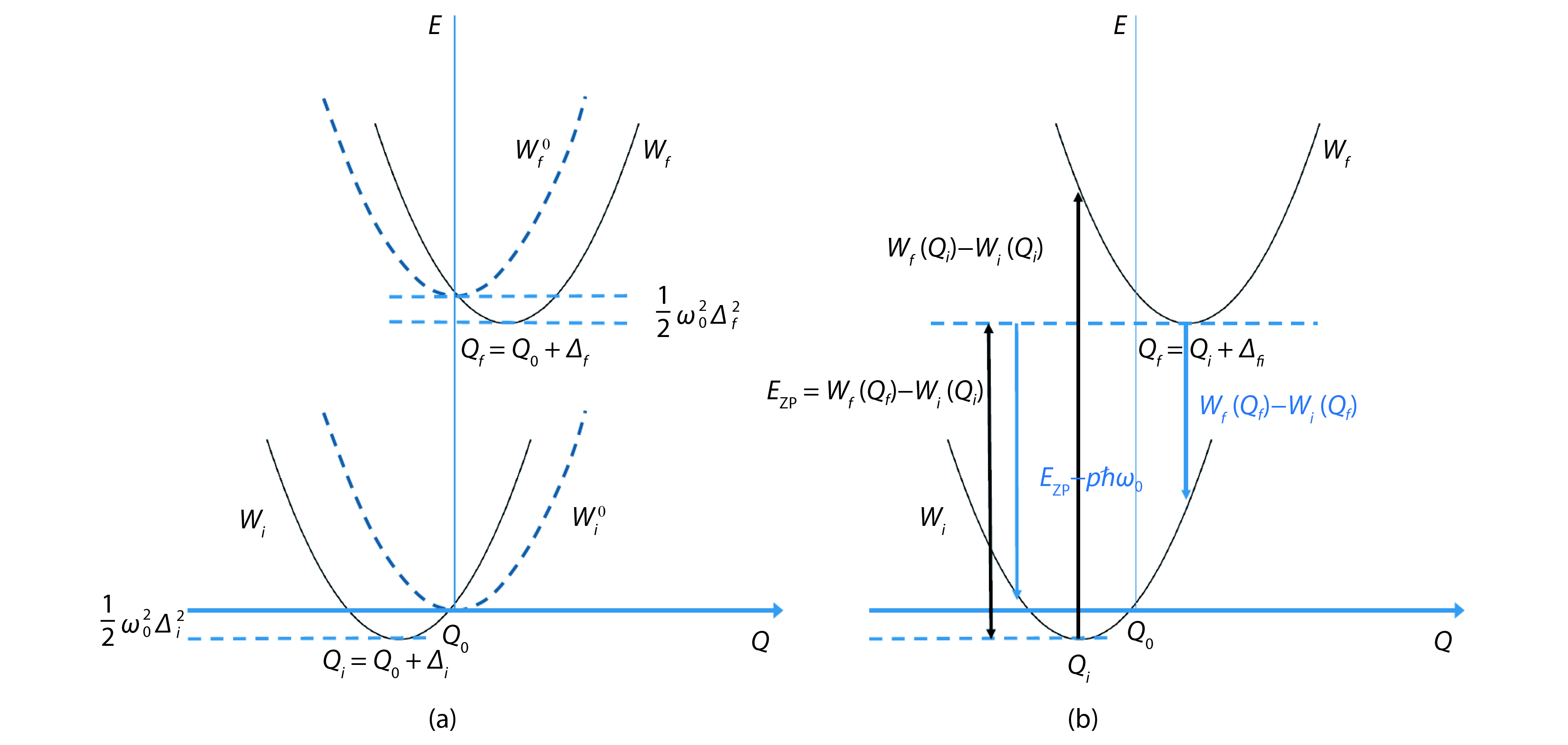
Fig. 1 is a configuration coordinate model showing lattice relaxation parameters Δi, Δf, and Δfi, different energy levels, and transition energies. Under F-C approximation, the excitation energy required for the ϕi → ϕf transition is
, which is higher than the zero-phonon energy
given by Eq. (10) or Eq. (12). However, zero-phonon transition is possible because of the finite overlap between the electronic wave functions ϕi(x, Qi) and ϕf(x, Qf). Note that because the transition energy calculated by a self-consistent method corresponds to the zero-phonon energy, for a defect structure with strong lattice relaxation, the excitation energy required to efficiently excite the electron from the ground state to the excited state could be significantly higher than the calculated transition energy. This consideration is relevant to, for instance, an acceptor state with strong lattice relaxation between the neutral (empty) and ionized (occupied) state, where thermal activation energy could be significantly higher than the calculated transition energy (assuming it is not limited by computational accuracy).

Figure 1.(Color online) Illustration of a configuration coordinate model. (a) Energy levels before and after taking into account the lattice relaxation. (b) Transition energies in relaxed configuration coordinates.
In calculating the transition matrix element Mfi(Q) from Eq. (14), we have neglected the potential effect of HeL in the electronic states or used the zeroth-order electronic wave functions. However, if we treat HeL as a perturbation in the electronic wave function, Mfi(Q) itself can lead to multiple phonon transitions. Applying the first order perturbation of HeL to the electronic wave functions, i.e., keeping the linear terms like
,
as the intermediate states that can couple to the final state
, Mfi(Q0) calculated with such mixed electronic states will result in emitting or absorbing one phonon[8]. This is equivalent to treating HeL + HeR as a second-order perturbation in the electronic states. If ϕf is a bulk state, the momentum conservation is required between ϕj(kj) and ϕf(kf) and only the phonon(s) with q equal or close to kf – kj can participate in the transition, which is the origin of the MC model. This process is relevant to the indirect bandgap transition where the effects on the phonon wave functions are typically neglected (i.e., < χin|χfn'> =δn,n’). Indeed, the lattice relaxation for a bulk state is practically zero, as will be discussed below. However, if ϕf is an impurity state and expressed as a superposition of band states
, then
. If the intermediate state
is a bulk state, then
can potentially be non-zero for any phonon mode with q = k – kj (because the impurity state does not have a well defined kf), thus, resulting in a spectrum with various one-phonon bands. This extended MC model was proposed to explain the phonon sidebands associated with the deformation potential interaction in GaP:N[15], but it was pointed out later that this model cannot yield correct coupling strengths, albeit capable of reproducing the general shape of the phonon-side band spectrum[6].
3.2. Huang–Rhys factor for bulk states
It was mentioned in the Introduction that lattice relaxation is not applicable to the transition between two bulk states. Mathematically, one can see that for a bulk state |nk> the matrix elementΔk(q) = < nk|u(q)|nk> ∝δq,0; and for q = 0, < nk|u(q)|nk> ∝ <nk|nk>, which is essentially the normalization condition and will be the same for all |nk> states. Thus, the lattice relaxation is negligible for a Bloch state[16], and similarly, the relative lattice relaxation between any two bulk states has Δk1,k2(q) = Δk1(q) – Δk2(q) = 0. This conclusion is expected to be valid also for typical nanostructures where the electronic wave function of the quantum confined state can be approximated by a bulk state modulated by an envelope function that is much larger than the unit cell size.
For a free exciton, the lattice relaxation should also normally be zero. We may use a Slater determinant Ψ0 to describe the ground state of the system, where all k states are occupied by the valence electrons. For simplicity, we consider a free exciton state in a direct band gap semiconductor with kex= 0. The wave function of the excitonic state Ψex can be expressed as a superposition of excited states Ψvk,ck with coefficients Ak where each Ψvk,ck is a Slater determinant with one valence band state |vk> being replaced by a conduction band state |ck>, meaning that one electron has been excited to the conduction band[9]:
${\varPsi _{{\rm{ex}}}} = \mathop \sum \nolimits_{{k}} {A_k}{\psi _{vk,ck}}.$
(16)
For a large Wannier exciton, Ak will be the Fourier components of the exciton envelop function φ(r = re – rh). Including the electron–phonon interaction for all electrons as
, the lattice relaxation can be calculated by evaluating
, which yields
${\varDelta _{{\rm{ex}}}}\left( {{q}} \right) = \frac{1}{{\omega _0^2}}\mathop \sum \nolimits_k {\left| {{A_k}} \right|^2}\left(\left\langle {ck\left| {{u_q}} \right|ck} \right\rangle - \left\langle {vk\left| {{u_q}} \right|vk} \right\rangle\right).$
(17)
As
, we have Δex(q) = 0, i.e., no lattice relaxation for a free exciton. Alternatively, if we assume a large Wannier exciton with its wave function containing only k states near k0, we can move Δck,vk(q) to the outside of the summation and notice that
. Then
. Here a polaron effect has been neglected. For a largeWannier exciton, the polaron effect is similarto the MC model to include the HeL induced mixing or scattering of different k states.However, for a bound exciton involving one highly localized particle, the lattice relaxation can be non-zero. For instance, if an electron is bound to a highly localized impurity center, and the hole is attracted to the bound electron, the lattice relaxation is given as[6]
${\varDelta _{{\rm{ex}}}} = \frac{1}{{\omega _0^2}}\left( {\left\langle {{\phi _i}\left| {{u_q}} \right|{\phi _i}} \right\rangle - \mathop \sum \limits_{{k}} {{\left| {{A_k}} \right|}^2}\left\langle {vk\left| {{u_q}} \right|vk} \right\rangle } \right),$
(18)
where ϕi is the wave function of the impurity bound state, and Ak the k component of the wave function of the hole bound state. In this case,
is responsible for the appearance of phonon sidebands, since the contribution of the second term is practically zero. Limiting values of S factors for LO phonons with deformation and polar interaction were estimated for a highly localized defect state in a few III–V and IV semiconductors[16]. For instance, Sp ≈ 2.7 for GaAs and 2.1 for GaP. Applying the model to CdSe and ZnTe, the estimated limiting values will be Sp ≈ 7.3 and 4.9, respectively. These values were computed with the defect wave function extending over a range rT approximately 2.5 times the lattice constant. Since Sp scales inversely with rT, the model suggests Sp → 0 as rT → ∞, indicating that there is again no lattice relaxation for a free particle. Similarly, in the case of a bound exciton due to alloy fluctuation in a semiconductor alloy, the lattice relaxation or S factor associated with the deformation potential was found to be inversely proportional to the number of unit cells occupied by the electron and hole wave function[17].
In the literature, there are some theories that imply or claim non-zero lattice relaxation or Huang–Rhys factor for a free or bulk exciton, either assuming Δck,vk(q) ≠ 0[18] or calculating Δ(q) with the exciton envelop function (for the electron–hole relative motion)[19, 20]. The model of Ref. [19] yielded Sp = 0.38–1.4 for CdSe and 0.008 for GaAs for the polar (Fröhlich) interaction in the bulk crystal. The theory was further used to calculate the size dependence of Sp in nanostructures[19, 21]. The other model calculated the lattice relaxation, and thus the Huang Rhys factor for a bulk exciton by assuming a highly localized hole and an electron in a hydrogentic state described by the exciton envelop function[20]:
${\varDelta ^2} = \frac{{{e^2}}}{a}{\left( {\frac{{24}}{{\text{π}} }} \right)^{1/3}}\frac{{\left( {\varepsilon _\infty ^{ - 1} - \varepsilon _0^{ - 1}} \right)}}{{{\omega _{\rm LO}}}}\frac{1}{w}\mathop \int \nolimits_0^w \frac{{{x^4}{{\left( {2 + {x^2}} \right)}^2}}}{{{{\left( {1 + {x^2}} \right)}^4}}}{\rm{d}}x,$
(19)
where
,
is the exciton Bohr radius, and
is the lattice constant. This model has yielded large Huang–Rhys factors for polar interaction in various bulk materials, for instance Sp ≈ 4.5 for CdS and CdSe[22], and Sp = 3.2 for ZnTe[23]. A modified model was used to study the S factor in quantum confined structures[24]. The primary problem of these models[19, 20] appears to be that they use an inappropriate charge density for the free or bulk exciton. These results gave the wrong impression that the bulk material could have a large S factor, which might have prompted the use of the so-called A term in Albrecht’s theory to explain the appearance of multiple LO phonon peaks in resonant Raman scattering in the bulk material, and further in nanostructures. This issue will be discussed further in Section 4.
3.3. An example of applying Huang–Rhys theory
As example of an application of Huang–Rhys theory, Fig. 2 shows a PL spectrum for radiative recombination of an exciton bound to an isolated nitrogen impurity in a lightly doped GaP:N. This is one of the most well-studied impurity systems, and the best studied isoelectronic impurity system in semiconductors. This is a case of relatively weak or moderately strong electron–phonon coupling with S factors smaller than 1 for all phonon modes, where the LO(Γ) sideband is due to the Fröhlich interaction while the X sideband as well as the TA and LA sidebands are due to the deformation potential interaction. This has been used as an example to illustrate that the CC and MC models might both be able to yield multiple phonon side bands, but only the CC model can give rise to S factors that are quantitatively consistent with experimental results[6]. A Koster-Slater on-site potential model (a likely oversimplified theory)[25], was used to calculate the electronic bound state of the N impurity. Incidentally or non-incidentally, it was found that when the electron binding energy Ee was around 6 meV, the calculations yielded respectively the correct exciton binding energy of the bound exciton[26] and the strengths of the exciton–phonon coupling for both deformation and polar interaction[6]. A density-functional theory based on a local density approximation (plus charge patching) yielded an Ee of 8 meV[27], whereas it is known that Ee < 11 meV from the experimentally measured difference between the free-exciton and bound-exciton transition energy. In general, a quantitative calculation of S factors is traditionally non-trivial without making many approximations. It has recently become more feasible with the development of a more sophisticated theoretical approach[28]. With the availability of clean and unambiguous experimental data and a solid understanding of the underlying physics, exciton-phonon coupling in GaP:N may serve as a testbed for a new computational method or technique.
Figure 2.(Color online) Photoluminescence spectrum of the isolated nitrogen bound exciton in GaP:N (4.2 K, [N] = 1016 cm-3, A line at 2.317 eV)[6].
4. Albrecht’s theory for Raman scattering
Huang–Rhys theory applies the first-order perturbation of HeR to an electronic transition between two coupled states approximated by
and
. Albrecht’s theory instead applies the second order perturbation of HeR to describe a Raman scattering process[5]. Besides the added complexity of the second order perturbation, the latter theory in its general form involves both electronic and vibrational intermediate states, and also includes HeL in both electronic and vibrational states. Thus, it is expected to be much more complex than Huang–Rhys theory.
We offer a concise summary of Albrecht’s theory below, attempting to use the same conventions as adopted in Huang–Rhys theory but using as closely as possible the same symbols used in Albrecht’s original paper. For the transition between two states of the molecular system |m> = |ψm> → |n> = |ψn>, the polarizabilityαnm of Eq. (2) in the original paper is reproduced below (for simplicity, we neglect the light polarization index):
${\alpha _{nm}} = \frac{1}{\hbar }\mathop \sum \nolimits_r \left(\frac{{{M_{nr}}{M_{rm}}}}{{{\omega _{rm}} - {\omega _0}}} + \frac{{{M_{rm}}{M_{nr}}}}{{{\omega _{rn}} + {\omega _0}}}\right),$
(20)
where
ω0 is the photon energy,
ωrm is the energy difference between the two states |r> and |m>, andMrm = < r|HeR|m>. The Raman scattering of interest is that a molecule at the initial statem = gi (|g> being the electronic ground state and |i> the vibrational state) is excited by the photon of frequencyω0 to some intermediate state r = ev, and returns to the state n = gj (i.e., the same electronic ground state |g> but a different vibrational state |j>) after emittingj–i phonons of one particular phonon mode. Since the second term in Eq. (20) is not practically useful for the problem of interest, it will be omitted thereafter. αnm can be rewritten using separated indexes for electronic and vibrational states:
${\alpha _{gj,gi}} = \frac{1}{\hbar }\mathop \sum \nolimits_{ev} \frac{{{M_{gj,ev}}{M_{ev,gi}}}}{{{\omega _{ev,gi}} - {\omega _0}}}.$
(21)
Under the Born-Oppenheimer approximation, the relevant molecular states can be expressed as
, and ψn = ϕg(x,Qi)χj(Qi). The difference between χi(Qi) and χj(Qi) is only in phonon occupation number, but there can be lattice relaxation between the ground state and intermediate states. The matrix element is
${M_{rm}} = {M_{ev,gi}} = \left\langle {{\chi _{ev}}\left| {{M_{e,g}}\left( Q \right)} \right|{\chi _{gi}}} \right\rangle ,$
(22)
with the electronic transition matrix element of
${M_{e,g}}\left( Q \right) = \left\langle {{\phi _e}\left| {{H_{\rm eR}}} \right|{\phi _g}} \right\rangle .$
(23)
Now keeping the HeL induced electronic state mixing to the first order, we have
${M_{e,g}}\left( Q \right) = M_{e,g}^0 + \mathop \sum \nolimits_s {\lambda _{e,s}}\left( Q \right)M_{s,g}^0,$
(24)
where
is the matrix element under F-C approximation as in the Huang–Rhys theory or CC model, λe,s(Q) terms are linear in Q, similar to those electronic mixing terms in the MC model, and the summation in the second term is over electronic state index s (another summation over vibrational modes in λe,s(Q) is not written out explicitly[5]). With
given by Eq. (24), the total matrix element of Eq. (22) becomes
${M_{ev,gi}} = M_{e,g}^0\left\langle {{\chi _{ev}}|{\chi _{gi}}} \right\rangle + \sum\nolimits_s {M_{s,g}^0} \langle {\chi _{ev}}|{\lambda _{e,s}}\left( Q \right)\left| {{\chi _{gi}}} \right\rangle .$
(25)
After substituting Eq. (25) into Eq. (21), the polarizability is given below with two terms (the Cterm in Albrecht’s paper associated with the second term in Eq. (20) no longer exists):
$
{\alpha _{gi,gj}} = A + B,
$
(25)
where
$A = \frac{1}{\hbar }\sum\nolimits_{ev} {\frac{{|M_{e,g}^0{|^2}\left\langle {{\chi _{gj}}|{\chi _{ev}}} \right\rangle \left\langle {{\chi _{ev}}|{\chi _{gi}}} \right\rangle }}{{{\omega _{ev,gi}} - {\omega _0}}}} ,$
(26)
$B = \frac{1}{\hbar }\sum\nolimits_{ev} {\sum\nolimits_s {\frac{{M_{g,e}^0M_{s,g}^0\left\langle {{\chi _{gj}}} \right.\left| {\left. {{\chi _{ev}}} \right\rangle \left\langle {{\chi _{ev}}} \right.} \right|{\lambda _{e,s}}|\left. {{\chi _{gi}}} \right\rangle + M_{e,g}^0M_{s,e}^0\left\langle {{\chi _{ev}}} \right.\left| {\left. {{\chi _{gi}}} \right\rangle \left\langle {{\chi _{gj}}} \right.} \right|{\lambda _{s,g}}|\left. {{\chi _{ev}}} \right\rangle }}{{{\omega _{ev,gi}} - {\omega _0}}}} } .$
(27)
In the case of
, corresponding to the below bandgap non-resonant excitation, one can assume that
and
are constants, and
, after applying the sum rule
. The A term cannot yield any change in the vibrational state, thus, corresponding to Rayleigh or elastic scattering. The
term in B involves the first-order matrix element of HeL induced electronic state mixing and an energy denominator such as
, which effectively makes it a third-order perturbation theory. Therefore, B will contribute to the transition of emitting or absorbing one phonon, and after making
, it is essentially the same as the conventional Raman cross-section[10].
Under a near resonant condition, i.e.,
for one electronic intermediate state ϕe, we can keep only one electronic state in the summation in the A term, which results in the A''' term in Albrecht’s paper:
$A''' = \frac{1}{\hbar }\mathop \sum \nolimits_v \frac{{|M_{e,g}^0{|^2}\left\langle {{\chi _{gj}}} \right|\left. {{\chi _{ev}}} \right\rangle \left\langle {{\chi _{ev}}} \right|\left. {{\chi _{gi}}} \right\rangle }}{{{\omega _{ev,gi}} - {\omega _0} + i{\gamma _e}}},$
(28)
where γe is a damping constant for electronic state ϕe. Now the summation over the phonon modes can in-principle include those not contributing to the Raman scattering of interest (e.g., there might be more than one branch of LO phonons)[29], but normally people only consider the specific phonon mode that is measured. The corresponding B term under resonance is referred to as B''', which is not explicitly given here.
Although the original theory was developed for Raman scattering of molecules, it has often been adopted for describing (resonant) Raman scattering in solids. For the later purpose, we further simplify A''' to a familiar form that is typically used in the literature to describe the resonant Raman scattering of LO phonons in bulk and nanoscale semiconductors. By letting
,
, and
, we have the polarizability for emitting n phonons as
$A = |M_{e,g}^0{|^2}\mathop \sum \nolimits_m \frac{{\left\langle {n\left| m \right\rangle \left\langle m \right|0} \right\rangle }}{{{E_{e,i}} + m\hbar {\omega _{\rm LO}} - {\omega _0} + i{\gamma _{\rm e}}}}.$
(39)
Albrecht stated that even under the resonance condition, “it is reasonable to expect that B''' is still responsible for most of the Raman effect while A''' leads primarily to Rayleigh scattering”[5]. It was also pointed out by Cardona that “for solids and large molecules, … the vibrational functions of initial and intermediate states are orthonomal and no Raman scattering usually results from the A-terms”[3]. This is consistent with the discussions given in the previous section that there should be no lattice relaxation between bulk states. Therefore, the A''' term cannot yield the multi-phonon peaks of resonant Raman scattering in either bulk or typical nanostructured semiconductors, unless the nanocrystals are extremely small or the resonant state is a highly localized defect/impurity state. Unfortunately, theories like Eq. (30) have often been used to describe the resonant Raman phenomenon in both bulk and nanoscale semiconductors[20, 22–24, 30, 31], which is ultimately based on the belief that there is considerable lattice relaxation, thus < m|0> ≠ 0 even in the bulk. This is in turn based on the model of Eq. (19) that predicts a large lattice relaxation for a bulk exciton[20]. There is one exception indicating that Huang–Rhys factor was in fact very small, on the order of 10–3, in CdSe nanocrystals, and that the experimental observed resonant phenomenon (although not quantitatively the relative intensities of the nLO peaks) could be explained by a theory without resorting to lattice relaxation[32]. In fact, there are other theories in the literature that have been developed for modeling the resonant Raman phenomena in bulk materials, such as one involving different excitonic states as intermediate states, which may explain the intrinsic nature of the very weal 1LO peak in bulk ZnTe and CdSe[2]. With this understanding, the relative enhancement of the 1LO peak to the 2LO peak implies the degradation of material crystallinity due to increase in bulk or surface defects, rather than a reduction in Huang–Rhys factor by using the A''' based model. As an example, Fig. 3 compares two Raman spectra of ZnTe excited with a 532 nm laser (close to its bandgap) between a high quality single crystalline sample and a defective thin-film grown on a Si (211) substrate, where in the latter the 1LO Raman peak is drastically enhanced relative to the 2LO peak (the I2LO/I1LO ratio changes from around 10 to 0.7)[33]. Therefore, it is important to obtain the intrinsic result, which might not be trivial, to validate a theory. A secondary issue found in the literature is that, in Eq. (30), the index m for the intermediate states in the denominator was sometimes replaced by n for the final state[22, 23, 30], which incorrectly simplified the result to
, after applying the sum rule. Since both
and
are of the ground state, thus
, one would have A''' = 0 for n ≠ 0.
Figure 3.(Color online) Resonant Raman spectra of ZnTe measured by a 532 nm laser at room temperature for one high quality single crystal sample and a thin-film sample grown on a Si (211) substrate. Strong PL background of the single crystal sample has been removed.
When lattice relaxation does exist, such as when the intermediate state is a highly localized state, the A term can in principle induce multi-phonon transitions. Resonant Raman studies on isoelectronic impurity bound exciton states of isolated N and NN pairs in GaP:N were conducted[34, 35], but no multi-phonon scattering was reported. Under incoming resonance, the 1LO Raman signal was much weaker than the PL signal of the LO sideband, which makes it impractical to see the effect if it is indeed present. However, it has been found that when the excitation energy is in resonant with a bulk critical point in a semiconductor alloy or a semiconductor with heavily doped isoelectronic impurities, 2LO and associated Raman peaks are strongly enhanced[14], and even nLO peaks can be observed[36]. In these cases, 1LO peak tends to be the strongest. The effect has been explained as disordering induced lattice relaxation[14, 17]. Even a formalism resembling Eq. (30) was used[14], although the applicability was not well justified.
In short, A''' is not appropriate to be used as a framework to explain resonant Raman scattering and the size dependence of Huang–Rhys factor. Lattice relaxation can in-principle be involved in resonant Raman scattering, but typically it is expected to be rather small and involved in a very subtle manner mostly through the B''' term like mechanisms. In reality, the changes in the relative intensity of nLO resonant Raman peaks are mostly extrinsic in nature rather than the quantum confinement induced change in electron–phonon coupling.
5. Summary
We have provided a concise review of Huang–Rhys theory applied to optical transitions involving localized electronic states in semiconductors and Albrecht’s theory for Raman scattering originally developed for molecules but also frequently used in solids.
There are two commonly adopted approaches to dealing with electron–phonon coupling in optical transitions. One approach treats the coupling in the vibrational states, as in Huang–Rhys theory, which leads to static lattice relaxation or displacement as well as multi-phonon transitions in emission and absorption spectra involving highly localized defect or impurity states where a Huang–Rhys factor S can be used to describe the coupling strength. The other approach treats the coupling in the electronic states, such as in the theory of an interband optical transition in an indirect bandgap semiconductor where the dynamic lattice displacement is relevant. For bulk single particle states as well as free exciton states, the lattice relaxation effect should be practically zero. The connection between a self-consistent first-principles calculation and Huang–Rhys model is also discussed.
Huang–Rhys theory is a first-order perturbative treatment of electron-electromagnetic field coupling, and it is intended for applications in absorption and PL spectroscopy. Albrecht’s theory is intended for Raman scattering, and in its most general form it is a second-order perturbative treatment of the electron-electromagnetic field coupling that may take into account both the electronic and vibration intermediate states and include the electron–phonon coupling in both the electronic and vibrational part. The A term in Albrecht’s theory is fundamentally related to Rayleigh scattering, although with lattice relaxation it could contribute to multi-phonon scattering. However, in reality, if only bulk states are involved, the lattice relaxation effect should be zero. Therefore, it normally cannot be used to describe the resonant Raman scattering of LO phonons in bulk and nanostructured semiconductors. The B term, involving the electron–phonon coupling induced mixing of electronic states, is similar to the conventional Raman scattering theory. To a large extent, when applied to a solid state, the lattice relaxation effects in Albrecht’s theory can be neglected. However, to properly explain the experimental results of resonant Raman scattering, some excitonic states are likely required to be included as the intermediate electronic states.
Acknowledgments
It is a great honor to be invited to contribute this article to the special issue of the Journal of Semiconductors in celebrating Prof. Kun Huang’s 100th birthday anniversary. I would like to take this opportunity to express my sincere gratitude to Prof. Jiansheng Zheng of Xiamen University and Prof. Michael D. Sturge of Dartmouth College for their guidance and support when I was a graduate student in their groups where I had the opportunity to study the effects of electron–phonon coupling in nitrogen bound excitons in GaP. I am very grateful to many other collaborators at Xiamen University, Institute of Semiconductors, Dartmouth College, and National Renewable Energy Laboratory, in particular to Prof. Weikun Ge for his longtime friendship and collaboration on the subject. I would also like to thank my group members at UNC-Charlotte, particularly Dr. Yingyan Yi and Dr. Jason Marmon, for their contributions in studying resonant Raman effects in II–VI compounds and their nanostructures.
References
[1] K Huang, A Rhys, N F Mott. Theory of light absorption and non-radiative transitions in F-centres. Proc Royal Soc London A, 204, 406(1950).
[2] S Permogorov. Excitons. North-Holland Publishing Company, 177(1982).
[3] M Cardona. Light Scattering in Solids II. Springer Berlin Heidelberg, 19(1982).
[4] S Z Karazhanov, Z Yong, L W Wang et al. Resonant defect states and strong lattice relaxation of oxygen vacancies in WO3. Phys Rev B, 68, 233204(2003).
[5] A C Albrecht. On the theory of Raman intensities. J Chem Phys, 34, 1476(1961).
[6] Y Zhang, W K Ge, M D Sturge et al. Phonon side-band of excitons bound to isoelectronic impurities in semiconductors. Phys Rev B, 47(1969).
[7] Y Zhang, W K Ge. Behavior of nitrogen impurities in III–V semiconductors. J Lumin, 85, 247(2000).
[8]
[9] F Bassani, G P Parravicini. Electronic states and optical transitions in solids. Oxford: Pergamon, 190(1975).
[10]
[11]
[12]
[13] K Huang. Lattice relaxation and theory of multiphonon transitions. Prog Phys, 1, 31(1981).
[14] M Balkanski. Effects of electron–phonon interaction in luminescence and light scattering. J Lumin, 24/25, 381(1981).
[15] P G Snyder, C W Myles, H H Dai et al. Model for phonon-assisted indirect recombination at impurity sites in semiconductors: A test of impurity wave-function theories. Phys Rev B, 32, 2685(1985).
[16]
[17] Y L Wang, Z Q Gu, K Huang. A disorder induced lattice relaxation mechanism in alloys. Chin Sci Bull, 26, 531(1981).
[18] S Schmitt-Rink, D A B Miller, D S Chemla. Theory of the linear and nonlinear optical properties of semiconductor microcrystallites. Phys Rev B, 35, 8113(1987).
[19] S Nomura, T Kobayashi. Exciton--LO-phonon couplings in spherical semiconductor microcrystallites. Phys Rev B, 45, 1305(1992).
[20] R Merlin, G Güntherodt, R Humphreys et al. Multiphonon processes in YbS. Phys Rev B, 17, 4951(1987).
[21] R Heitz, I Mukhametzhanov, O Stier et al. Enhanced polar exciton-LO-phonon interaction in quantum dots. Phys Rev Lett, 83, 4654(1999).
[22] A P Alivisatos, T D Harris, P J Carroll et al. Electron–vibration coupling in semiconductor clusters studied by resonance Raman spectroscopy. J Chem Phys, 90, 3463(1989).
[23] Q Zhang, J Zhang, M I B Utama et al. Exciton–phonon coupling in individual ZnTe nanorods studied by resonant Raman spectroscopy. Phys Rev B, 85, 085418(2012).
[24] M C Klein, F Hache, D Ricard et al. Size dependence of electron–phonon coupling in semiconductor nanospheres: The case of CdSe. Phys Rev B, 42, 11123(1990).
[25] R A Faulkner. Toward a theory of isoelectronic impurities in semiconductors. Phys Rev, 175, 991(1968).
[26] Y Zhang. Acceptor-like bound excitons in semiconductors. Phys Rev B, 45, 9025(1992).
[27] Y Zhang, A Mascarenhas, L W Wang. Systematic approach to distinguishing a perturbed host state from an impurity state in a supercell calculation for a doped semiconductor: Using GaP:N as an example. Phys Rev B, 74, 041201(2006).
[28] L Shi, L W Wang. Ab initio calculations of deep-level carrier nonradiative recombination rates in bulk semiconductors. Phys Rev Lett, 109, 245501(2012).
[29] P M Champion, A C Albrecht. Investigations of Soret excited resonance Raman excitation profiles in cytochrome c. J Chem Phys, 71, 1110(1979).
[30] G Scamarcio, V Spagnolo, G Ventruti et al. Size dependence of electron–LO-phonon coupling in semiconductor nanocrystals. Phys Rev B, 53, R10489(1996).
[31] A M Kelley. Resonance Raman overtone intensities and electron–phonon coupling strengths in semiconductor nanocrystals. J Phys Chem A, 117, 6143(2013).
[32] R Rodríguez-Suárez, E Menéndez-Proupin, C Trallero-Giner et al. Multiphonon resonant Raman scattering in nanocrystals. Phys Rev B, 62, 11006(2000).
[33]
[34] M P Dos Santos, C Hirlimann, M Balkanski. Local induced activity in resonant Raman scattering of GaP:N. Phys B + C, 117/118, 108(1983).
[35] A Frommer, n E Cohen, n A Ron. Resonant Raman-scattering induced by excitons bound to nitrogen impurities in GaP:N. Phys Rev B, 47, 1823(1993).
[36] P H Tan, u Z Y Xu, o X D Luo et al. Resonant Raman scattering with the E+ band in a dilute GaAs1–xNx alloy (x = 0.1%). Appl Phys Lett, 89, 101912(2006).