
Xiaolun Xu, Aurélie Broussier, Tiziana Ritacco, Mackrine Nahra, Fabien Geoffray, Ali Issa, Safi Jradi, Renaud Bachelot, Christophe Couteau, Sylvain Blaize. Towards the integration of nanoemitters by direct laser writing on optical glass waveguides[J]. Photonics Research, 2020, 8(9): 1541
- Photonics Research
- Vol. 8, Issue 9, 1541 (2020)
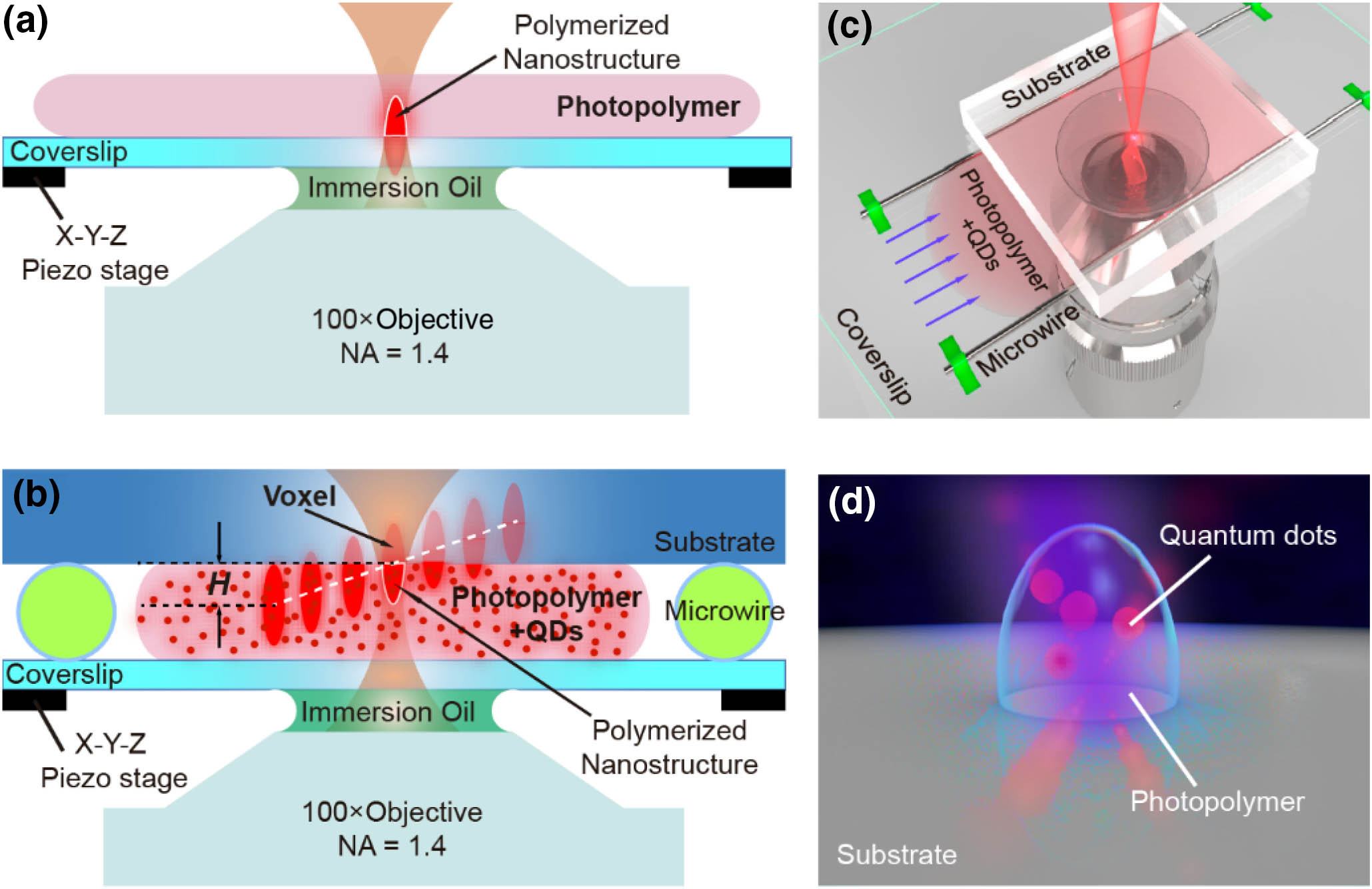
Fig. 1. (a) Schematic of the conventional DLW-TPP platform. (b), (c) Cross section and 3D illustration of our developed DLW-TPP platform for thick substrates. The red dots represent QDs dispersed inside the polymer liquid. The white dashed line shows the control of the laser focus height, which is indicated with H
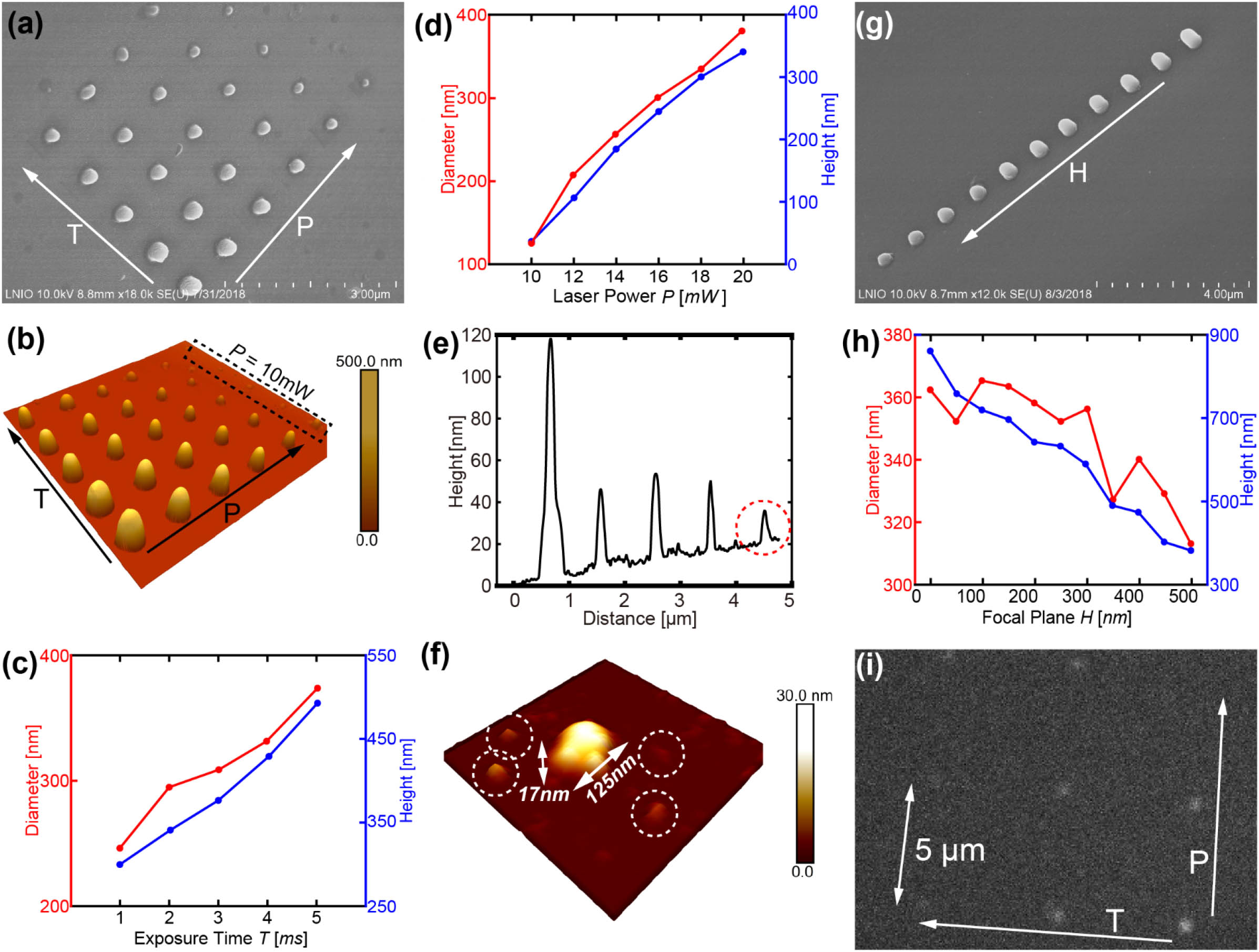
Fig. 2. Characterization of QD-polymer voxels. Tilt-view (a) SEM image and (b) AFM image of the voxel array with laser powers P T H P T P = 20 mW T = 5 ms P = 10 mW T = 1 ms H P = 20 mW T = 5 ms
Fig. 3. (a) SEM image of IEWs coated with a 4 nm thick conducting carbon layer. The schematic 3D view of the IEWs is shown in the inset. Integration of single QD-polymer voxels (b) on top and at the center of different waveguides and (c) several on the same waveguide, respectively. (d) SEM image of a single QD-polymer voxel on a single IEW; the inset shows the enlarged SEM image of the structure. (e) Far-field emission of the voxel in (d). The white dashed line indicates the outline of the IEW.
Fig. 4. (a) Schematic of QD emission measurement. (b) Spectrum of far-field emission emitted from the single QD-polymer nanostructure on the IEW with a Gaussian fit (red line). (c) Normalized extracted spectrum collected from the waveguide facet by a single mode fiber. The black line is for the nanoemitters placed on the IEW, while the gray line is for the IEW without nanoemitters on top.
Fig. 5. (a)–(d) Fabrication of a single layer of QDs by controlling laser printing parameters ( P , T , H )
Fig. 6. Relationship between QD concentration and far-field PL of QD-polymer voxels.
Fig. 7. (a) Refractive index distribution of the IEW. (b) | E |
Fig. 8. (a) Experimental fiber-IEW coupling stage. (b) Fiber coupled with the IEWs sample. (c) Microcopy image of fiber-IEWs coupling, enlarging the yellow dashed square in (b). (d) Coupled alignment laser scattered by QD-polymer voxel. White dashed line represents the corresponding waveguide.
Fig. 9. QD-IEW coupling efficiency as a function of the QD position along (a) x z
Fig. 10. (a) Schematic of an ensemble PL spectrum that consists of the individual QD emission spectrum convolved with the interparticle inhomogeneities. (b) Simulated transmission spectrum for 11 QDs emission coupled into IEW propagating modes.

Set citation alerts for the article
Please enter your email address
© Copyright 2018-2021 | Chinese Laser Press. All Rights Reserved 沪ICP备15018463号-20