Abstract
A major challenge towards nanophotonics is the integration of nanoemitters on optical chips. Combining the optical properties of nanoemitters with the benefits of integration and scalability of integrated optics is still a major issue to overcome. In this work, we demonstrate the integration of nanoemitters positioned in a controlled manner onto a substrate and onto an optical ion-exchanged glass waveguide via direct laser writing based on two-photon polymerization. Our nanoemitters are colloidal CdSe/ZnS quantum dots (QDs) embedded in polymeric nanostructures. By varying the laser parameters during the patterning process, we make size-controlled QD-polymer nanostructures that were systematically characterized using optical and structural methods. Structures as small as 17 nm in height were fabricated. The well-controlled QD-polymer nanostructure systems were then successfully integrated onto a new photonic platform for nanophotonics made of an ion-exchanged waveguide. We show that our QDs maintain their light emitting quality after integration as verified by photoluminescence (PL) measurements. Ultimately, QD emission coupled to our waveguides is detected through a home-built fiber-edge coupling PL measurement setup. Our results show the potential for future integration of nanoemitters onto complex photonic chips.1. INTRODUCTION
Luminescent colloidal semiconductor quantum dots (QDs) have already proven to be promising solid-state nanoemitters in the fields of nanophotonics and quantum optics [1–8]. For the practical realization of scalable photonic devices, one of the key requirements is the ability to integrate QDs onto specific optical chip locations. Many approaches have been explored, including electron beam lithography (EBL) [9–12], capillary force [13,14], optical trapping [15,16], and atomic force microscopy (AFM) transfer methods [17,18]. However, these methods have some limitations such as complicated operations, high manufacturing costs, and multiple fabricating steps [19,20].
Direct laser writing (DLW) based on two-photon polymerization (TPP) has been employed for producing one-dimensional (1D), two-dimensional (2D), and three-dimensional (3D) arbitrary microscale and even nanoscale polymeric structures in a fast and simple manner with high positioning and laser writing accuracy [21–24]. In the conventional DLW-TPP process, a pulsed laser is tightly focused to a diffraction-limited spot within the volume of liquid photopolymers. Due to a two-photon absorption (TPA) process [25], photo-polymerization (crosslinking of photopolymer) is triggered to form arbitrary hollow 3D polymeric structures by scanning the laser. Recently, embedding nanoemitters into a photopolymer host matrix has been exploited to produce QD-polymer composites by photo-polymerization, which joins the active light-emitting property of QDs together with the technological feasibilities of the polymer matrix [26–29]. Au et al. and Shi et al. fabricated photonic structures based on QD-polymer nanocomposites [30,31]; however, integrating these QD-polymer nanocomposites onto the pre-existing or preselected waveguides is still a challenge. Photonic circuits made of glass and integrated with QD-polymer nanocomposites via DLW-TPP have not been reported so far.
In this work, we demonstrate the integration of photonic devices with nanoemitters via DLW-TPP. A development of a conventional DLW-TPP platform enables transferring of size-controlled QD-polymer nanocomposites onto preselected optical substrates with sub-micrometer-scale precision. We succeeded in creating single QD-polymer nanostructures on the top surface and at the center of ion-exchanged optical waveguides (IEWs). IEWs are interesting candidates for future nanophotonic applications as they are fairly easy to fabricate, are cheap, can be connected to an optical fiber, and can be fabricated in a scalable way [32]. We demonstrate the light coupling from the QDs inside the polymer into our waveguides via photoluminescence (PL) measurements. This work indicates a good prospect towards a practical realization of deterministic integration of nanoemitters onto complex photonic devices.
Sign up for Photonics Research TOC. Get the latest issue of Photonics Research delivered right to you!Sign up now
2. EXPERIMENTAL SECTION
The standard DLW-TPP process is executed with a Nanoscribe Professional GT printer [33,34], which is powered by a femtosecond near-infrared laser at 780 nm, operating with pulse duration, 80 MHz repetition rate, and maximum mean power of (measured after the focusing objective). Photoresist is drop-casted on a transparent glass coverslip mounted on piezoelectric translation stages imaged by a 100 times immersion oil high resolution optical microscope objective, as shown schematically in Fig. 1(a). In this conventional DLW-TPP configuration, a typical working distance of the oil immersion objective is less than 170 μm, which makes this approach be used only for thin substrates. If one wants to use this method on another substrate containing waveguides in plane or on a silicon on insulator (SOI) substrate, some developments are necessary in order to do DLW-TPP. Bückmann et al. proposed dipping the microscope objective directly into a special photoresist material [35]. However, commercially available oil immersion-type microscope objectives are not designed for direct use with the photoresist material instead of the immersion oil. Moreover, diversity of substrate shapes and sizes limits its mounting on standard substrate holders. Thus, a need exists for developing a DLW-TPP configuration that can transfer QD-polymer nanocomposites onto thicker optical substrates.
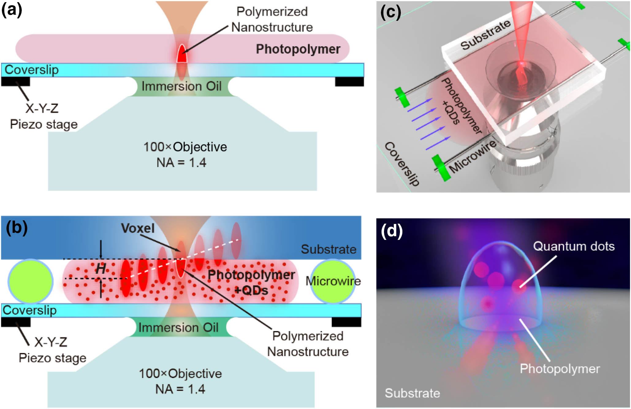
Figure 1.(a) Schematic of the conventional DLW-TPP platform. (b), (c) Cross section and 3D illustration of our developed DLW-TPP platform for thick substrates. The red dots represent QDs dispersed inside the polymer liquid. The white dashed line shows the control of the laser focus height, which is indicated with . (d) Schematic of a single QDs-polymer voxel presenting a typical oval shape.
Here, we used a DLW-TPP platform with a “sandwich” configuration for integrating QD-polymer nanocomposites on complex photonic chips, as shown in Figs. 1(b) and 1(c). The photosensitive polymer liquid is made by adding 1% of phenylbis (2, 4, 6-trimethylbenzoyl) phosphine oxide (IRG819) photoinitiator and 10% monomethyl ether hydroquinone (MEHQ) inhibitor into 1 mL pentaerythritol triacrylate (PETA) monomer containing 2 mg red QDs (CdSe/ZnS). The red QDs have an emission at 590 nm. First of all, two tungsten microwires with 25 μm diameters are placed directly between a coverslip and a face-down thick substrate (with diverse sizes and shapes) for creating a free space. Secondly, the polymer liquid containing QDs is placed into the space left by the wires thanks to the capillary force. Then, a laser is focused at the interface between the polymer liquid and the substrate during the patterning process. Finally, the non-exposed parts of the photopolymer liquid are subsequently removed using an acetone solution, resulting in a QD-polymer nanocomposite on the thick substrate, which is our ion-exchanged glass waveguide. The final QD-polymer nanocomposite (fabricated by the standard or our developed DLW-TPP method) is depicted schematically in Fig. 1(d).
3. RESULTS AND DISCUSSION
The oval-shape volume of the photo-polymerized resist inside the focused laser beam, called voxel [see schematic Fig. 1(d)], represents the ultimate resolution reachable during the DLW fabrication. Previous efforts for improving the precision of voxels by changing the laser writing power and the laser exposure time have been demonstrated on conventional DLW-TPP platforms [36–38]. With our developed sandwich platform, we can also control the laser power and exposure time . We systematically investigate the size of the QD-polymer nanostructures obtained with varying and by fabricating arrays of (with pitches of 1 μm) on silica substrates (). Figures 2(a) and 2(b) show, respectively, the scanning electron microscopy (SEM) and AFM images of the QD-polymer nanostructure voxels fabricated on a silica substrate. Clearly, it can be seen that by adjusting the laser power and exposure time the diameter and height of the voxels can be controlled with high spatial accuracy. The dependence of on the voxel dimensions (diameter and height) is shown in Fig. 2(c). The relationship between voxel size and laser power is shown in Fig. 2(d). As expected, diameter and height decrease along with the decreasing and . Consequently, this is an efficient way of controlling the volume of voxels by carefully adjusting and to control the amount of energy applied to the QD-polymer resin. The dimension of voxel structures can be scaled down to in height and in diameter (with , ), as shown in Figs. 2(e) and 2(f) by an AFM profile and image. In fact, four small “bumps” can also be observed in Fig. 2(f) (marked with white dashed circles), which are QDs surrounded by a polymer layer. That might be due to the thermal diffusion, which results in QDs being partially ejected outside the voxel during the TPP process. In this case, we can speculate that a handful of QDs should be trapped inside the polymeric voxel and 5 or 6 QDs are estimated by calculating the distribution density of QDs and the volume of the voxel (for detailed estimation of the number of QDs, see Appendix A).

Figure 2.Characterization of QD-polymer voxels. Tilt-view (a) SEM image and (b) AFM image of the voxel array with laser powers (10 to 20 mW using 2 mW steps) and exposure time (1 to 5 ms using 1 ms steps). The default value in this sample is 0 nm. (c), (d) Dependence of the height and diameter of single voxel structures in function of and , respectively. in (c), in (d). (e) AFM line profile of the QD-polymer voxels with marked with black dashed area in (b). The peak marked with the red dashed circle indicates the profile of the smallest voxel with , which is shown in the AFM image (not to scale) in (f). Four dots marked with white dashed circles are QDs surrounded by a polymer layer. Tilt-view (b) SEM image and (h) size dependence of an array of voxel structures by only changing the focal plane (0 to 500 nm using 50 nm steps), with and . (i) Measured PL image of a voxel array with 5 μm of distance between voxels.
In addition, as shown in Fig. 1(b), the DLW-TPP set-up is equipped with translation stages that allows tuning the laser focal position () during the patterning process. We thus fabricated an array of QD-polymer voxels to investigate the possibility for further reducing the voxel size, as shown in Fig. 2(g). The dependences of the voxel size on the laser focal height is shown in Fig. 2(h). We point out the potential of this control for the practical integration of single QDs inside these polymer nanostructures that can be positioned onto chips by simply changing the voxel volume, specifically by adjusting , , and . This method can be also used for fabricating a single layer of QDs (Appendix A). Another approach for reducing the QD number embedded in polymeric structures is to decrease QD mass concentration in the polymer liquid. We investigated this approach with three different concentrations of QDs and observed a decrease of PL as a function of the QD concentration as we would expect (see Appendix B).
The quantum efficiency of QDs might be degraded after the high temperature fabrication method. In our work, a ligand was introduced onto the QDs surface before preparing our polymer mixture for improving the QD stability and avoiding the photobleaching [33]. The PL image shown in Fig. 2(i) also reveals the stable light emission property of the QD-polymer nanocomposites, which makes it possible to use them as nanoemitters. In order to characterize the PL of these QD-polymer voxels, we also measured the PL emitted by each voxel. For that, we made an array of QD-polymer voxels with the distance large enough between the voxels (5 μm) so that we can avoid the illumination from the neighboring voxels. Figure 2(i) shows the far-field fluorescence image of the array excited by a light-emitting diode (LED) source emitting at 450 nm within an field of view. The emitting light was then filtered by a 530 nm long-pass filter and recorded by an electron-multiplying CCD camera. Bright points with different intensities are clearly visible and correspond to the QDs emission from voxels with different volumes. As we are able to control the size of the voxels at will, we can therefore control the number of QDs inside.
The refractive index of the pure PETA polymer changes from 1.485 to 1.52 before and after the DLW-TPP measured by spectroscopic ellipsometry [39,40]. It has been demonstrated that doping nanoparticles/QDs into the polymer matrix can increase the equivalent refractive index of the composites [41–43]. In our case, the bulk refractive index is 2.549 for CdSe and 1.533 for MEHQ. Therefore, it is speculated that the equivalent refractive index of the QD-polymer composites should be at least 1.52. A more accurate value can be obtained by a complex measurement, which should take into account not only the QDs doping ratio, but also the printing laser power and the homogeneity of QDs inside the composites.
One of the main motivations of this work is to create site-controlled QDs as nanosources for subsequent use in optical channels. Although the transfer of emission from QDs into optical circuits has been shown using various integration methods [44–46], DLW-TPP has never been used so far for realizing photonics devices with ion-exchanged glass waveguides. In order to confirm the potential of our developed approach in this context, we combined IEWs ( typical size) with our QD-polymer nanostructures acting as efficient light sources in the visible wavelength range. Figure 3(a) shows an SEM image of the IEWs. The 3D schematic of the IEW is shown in the inset of Fig. 3(a). Each waveguide has a width of about 2 μm, a depth of about 2 μm, and is separated from neighboring waveguides by . In our case, surface buried IEWs are beneficial for this application due to their flexibility to be tailored into various applications, with relatively simple and economic fabrication [32,47,48]. IEWs have a gradient index profile due to the index increment as ions diffuse further into the glass substrate to form waveguides (more details in Appendix C). Figure 3(b) shows the integration of QD-polymer nanostructures on different waveguides by controlling voxel parameters. Furthermore, Fig. 3(c) shows QD-polymer voxels integrated on the same waveguide. The results prove the ability of our method for controlling the position of the nanostructures with high precision. Figure 3(d) shows the SEM image of the QD-polymer nanostructure located at the center of the waveguide, which has the diameter of 347 nm and 335 nm in height measured by AFM. The enlarged details in the inset of Fig. 3(d) show its near semi-ellipsoid shape. A significant far-field QD emission is observed in Fig. 3(e) (red emission spot, filtered by a 580 nm long-pass filter). The results show evidence of the presence of QDs inside the polymer nanostructures and their stability of light emitting properties after the DLW-TPP process.
Figure 3.(a) SEM image of IEWs coated with a 4 nm thick conducting carbon layer. The schematic 3D view of the IEWs is shown in the inset. Integration of single QD-polymer voxels (b) on top and at the center of different waveguides and (c) several on the same waveguide, respectively. (d) SEM image of a single QD-polymer voxel on a single IEW; the inset shows the enlarged SEM image of the structure. (e) Far-field emission of the voxel in (d). The white dashed line indicates the outline of the IEW.
Figure 4(a) shows the schematic of QD emission radiated to the far field and coupled into the corresponding waveguide. Here, the QD-polymer voxel shown in Fig. 3(d) is used for measuring the emission using the two different configurations. The far-field QD emission can be collected by a multimode fiber towards a commercial portable spectrometer with a Peltier-cooled detector. The QD emission coupled to the IEW is collected by a facet-coupled fiber and detected by a CCD-cooled grating spectrometer (more measurement details are described in Appendix D). The recorded far-field spectrum shows an apparent peak at 588.5 nm with an FWHM of about 43.1 nm, which is indicative of our CdSe/ZnS QD-like emission signatures, as shown in Fig. 4(b).
Figure 4.(a) Schematic of QD emission measurement. (b) Spectrum of far-field emission emitted from the single QD-polymer nanostructure on the IEW with a Gaussian fit (red line). (c) Normalized extracted spectrum collected from the waveguide facet by a single mode fiber. The black line is for the nanoemitters placed on the IEW, while the gray line is for the IEW without nanoemitters on top.
Figure 4(c) shows the extracted spectrum from the side collection of the waveguides. We observe a narrow luminescence peak at 591.1 nm with an FWHM of about only 8 nm. The wavelength at maximum intensity is in very good agreement with the far-field spectrum presented above, which indicates that the QDs emission was coupled into the waveguide. The PL images were obtained and measured at the end of the waveguides (not shown). The spectrum with high intensity between 500 and 560 nm represents the 532 nm excitation laser, and the broad spectral emission between 600 and 700 nm is due to the fluorescence from IEW substrates itself. This is verified by the measured PL spectrum performed on a bare substrate IEW without the QD-polymer nanostructure, as plotted in the gray solid line. Interestingly, there is a strong discrepancy of PL spectrum FWHM between QD emission into the far field and into the IEW. This discordance is related to the dissimilarities in the PL measurement conditions. Because of the evanescence of the guided mode above the glass surface [49], it is expected that the QD-waveguide coupling efficiency decreases exponentially from the surface to the center of the polymer nanostructure (as simulated in Appendix E). As a consequence, only a few or perhaps even a single QD localized at a very short distance from the waveguide interface will be coupled to the waveguide. A single photon anti-bunching experiment would be required to assess the coupling of only a single QD. On the other hand, the far-field emission is collected from an ensemble of QDs embedded into the polymer voxel, and, as such, we obtained the typical emission due to different QD diameters [50]. This certainly causes an inhomogeneous broadening of the collected emission line shape [51–53], resulting in the broad QD emission peak in Fig. 4(b) (simulated results shown in Appendix F).
In addition, we also measured the waveguide-coupled QD emission for the QD-polymer voxels with different volumes on different waveguides. However, no significant QD emission was ever detected even for some larger and bigger voxels. This could be because in a bigger volume, the spatial distribution for QDs is larger, and there is less chance of finding a QD at the interface and at the right location on the waveguide. While for smaller voxels, embedded QDs are more concentrated near the surface, a small voxel means less embedded QDs and low-intensity emission. Further investigations need to be done in order to push the limits of the fabrication and characterization process and carefully control the number of QDs embedded in the polymeric nanostructures.
4. CONCLUSIONS
To conclude, we demonstrated the capability of the DLW-TPP method for enabling the positioning of nanoemitters on a thick substrate leading to the coupling of light to a photonic optical chip. Based on this technique, the control of three fabrication parameters, namely, the laser power, the exposure time, and the focal height, provides a control of the QD-polymer voxel size, which is strongly related to the volume of the voxels, all confirmed by far-field PL measurements. Single QD-polymer nanostructures have been successfully integrated at the center of an ion-exchanged optical glass waveguide for the first time, to the best of our knowledge. The QD emission was measured from the waveguide facet by our home-built measurement setup. The extracted spectrum of our QD emission showed a narrow peak at 590 nm, which is in good agreement with the far-field measurement results and suggests that the PL from only few QDs is efficiently coupled into the waveguide. This shows the high potential of QD-polymer nanostructures for nanosources of light positioned onto glass photonic circuits. Future work will focus on improvements of the emission efficiency from QDs into the waveguide to enable the efficient detection of single QD emission from the waveguide facet for smaller integrated QD-polymer nanostructures. Finally, our developed DLW-TPP technique opens an exciting route for the top-down deterministic integration of QD or other quantum emitters such as colored centers in nanodiamonds within future complex quantum photonic circuits.
Acknowledgment
Acknowledgment. The authors acknowledge the support of the Marie Skłodowska-Curie Actions Innovative Training Networks (MSCA-ITN) LIMQUET (Light-Matter Interfaces for Quantum Enhanced Technology); FEDER (Fonds Européen de développement régional), Grand Est Region and Graduate School EIPHI-BFC are acknowledged for their funding support of A. Issa’s postdoctoral fellowship (Nano-integration and PRONANO projects). X. Xu gratefully acknowledges the support of the Funding of China Scholarship Council (CSC). The authors thank the platform “Nanomat” for nanocharacterization.
APPENDIX A: FABRICATION OF SINGLE LAYERS OF QUANTUM DOTS
Based on our results for characterizing QD-polymer voxels systematically, the quantity of QDs embedded in polymeric structures is highly related to its volumes, which can be realized beyond the diffraction limit by our developed DLW-TPP platform. That way, we created single layers of QDs by carefully adjusting the laser parameters during the DLW-TPP process, shown in Figs.?5(a)–5(d). The measured height of the QD-polymer line is around 15?nm; this value is a bit larger than the average size of QDs (), which is because the QDs are surrounded by a polymer shell, as shown in Fig.?5(e). Thus, the QD-polymer line can be approximated by a single layer of QDs. Although the aggregation of QDs was observed in the inset of Fig.?5(e), the outline of each QD can still be roughly identified, which enables us to count the total number of QDs with this area. Thus, the QDs density can also be calculated by , with being the total number of QDs, which is 335 according to the Fig.?5(e), while is the area of the single layer of QDs, which can be calculated by (). The semi-ellipsoid voxel has the height of 17?nm, as shown in Fig.?2(f), which is roughly the same thickness of a single layer of QDs (15?nm). The area can be calculated by , where indicates the diameter of the voxel. Therefore, the calculated QDs number inside this voxel is 1.65 (rounded to two). There are a total of 5 or 6 QDs that can be estimated by taking into account the QDs outside and near this voxel, as shown in the Fig.?2(f). The PL of a single layer of QDs can also be detected, showing future potential applications in the context of hybrid LED devices, photonic crystals, and optical lasing [54–57].
Figure 5.(a)–(d) Fabrication of a single layer of QDs by controlling laser printing parameters . (e) SEM image of a single QD layer of the QD-polymer nanocomposite; this sample is the same as (d). The inset shows the detailed part marked with a yellow square.
APPENDIX B: EFFECT OF QD MASS CONCENTRATION ON FAR-FIELD PL
The effect of the QDs mass concentration in the photopolymer liquid was also investigated by far-field PL intensity. We made three liquid photo-polymerizable formulations with three different QD mass concentrations. is the original QD solutions dispersed in 1?g PETA monomer solution (used as polymer matrix), , and . We fabricated the voxels matrices using the same laser parameters (laser power 10–20?mW, exposure time 1–5?ms) for the three formulations and selected one voxel with a similar volume from each sample in order to analyze the difference of the emission between them. For each selected voxel, 40 repeated emission measurements with same measurement parameters have been done to obtain stable, accurate, as well as averaged spectra. As can be seen in Fig.?6, the QDs emission from the voxel structure decreases as the QDs mass concentration decreases. It is promising to obtain few or even single QDs inside a single polymeric voxel.
Figure 6.Relationship between QD concentration and far-field PL of QD-polymer voxels.
APPENDIX C: ION-EXCHANGED WAVEGUIDES AND THE INDEX MISMATCH
IEWs have been used for many optical and photonic applications due to the fact that they have low propagation loss (), are with low cost, can have single mode propagation in the visible spectrum, and are compatible with commercial fibers. In our work, the commercial IEWs (Teem Photonics) have a refractive index gradient distribution in glass due to the thermal diffusion of silver ions inside the glass substrate [32]. The highest refractive index of each IEW is around 1.57 with a refractive index for the glass around 1.5. That makes a significant index difference of , as shown in Fig.?7(a). This nonhomogeneous refractive index of IEWs may result in a local index mismatch, which could decrease the coupling of QD emission into the corresponding waveguide. Besides, there could also be an index mismatch between the effective refractive index of our QD-polymer nanocomposites and the IEWs, which reduces the coupling efficiency as well. An optimized equivalent refractive index can be obtained by adjusting the QDs mass concentration. Figure?7(b) shows finite-difference time-domain (FDTD) simulated results of a fundamental TE mode source propagating along this waveguide at 590?nm. The close proximity of the QD-polymer nanostructures and waveguide allows the energy transfer between QDs and IEWs through an evanescent wave coupling mechanism [58].
Figure 7.(a) Refractive index distribution of the IEW. (b) field cross-section distribution with a 590 nm TE propagating mode along the IEW; the white solid line indicates the amplitude distribution vertical to the interface.
APPENDIX D: PL MEASUREMENT SET-UP AND FIBER-WAVEGUIDE FACET ALIGNMENT
A home-built PL measurement set-up is used to detect the QD emission coupled to the IEW, as shown in Fig.?8(a). A 617?nm LED light source below the sample stage allows individual devices to be imaged. The input single mode fiber (mounted on an piezoelectric stage) is aligned at the end of the corresponding waveguide facet with a 640?nm continuous laser to optimize the fiber-IEW coupling. Some of the alignment light is scattered out of the waveguide plane. The spatial distribution of the light intensity along the waveguides is projected onto a CCD camera, and this allows us to observe the light propagation and to pre-align our waveguides with the optical fiber. Once the input fiber is properly aligned, the sample is excited from the top by switching an excitation laser at 532?nm through a 60 times microscope objective (numerical aperture, ). The QD emission coupled to the IEWs is collected and detected by a CCD-cooled spectrometer. The far-field QD emission can also be collected by a multimode fiber and directed through a 540?nm long-pass filter towards another commercial portable spectrometer.
Figure 8.(a) Experimental fiber-IEW coupling stage. (b) Fiber coupled with the IEWs sample. (c) Microcopy image of fiber-IEWs coupling, enlarging the yellow dashed square in (b). (d) Coupled alignment laser scattered by QD-polymer voxel. White dashed line represents the corresponding waveguide.
Pre-alignment of the fiber and of the waveguide ensures that we are able to measure the QD emission from the waveguide facet. The external 640?nm CW laser is focused into a fiber, and then coupled into the IEW. Fiber-waveguide coupling is achieved by adjusting the position of the fiber tip via a piezo electric translation stage. The leakage of propagating light along the waveguide makes it possible to optimize the coupling visualized by our home-made optical microscope. Figure?8(b) shows the experimental fiber-waveguide sample coupling stage, where the red light line on the IEW sample surface indicates the propagating 640?nm laser which in this case means a good coupling efficiency. Figure?8(c) shows the enlarged optical image from the yellow dashed square in Fig.?8(b). No scattering light between the fiber and the IEW is observed when the optical fiber mode and the IEW waveguide mode have a good overlap. At the position of the QD-polymer voxels on the waveguide placed far away from the waveguide input facet, a clear light spot is observed due to the guiding laser scattered by the structure, which helps us optimize the fiber-to-waveguide alignment, as shown in Fig.?8(d).
APPENDIX E: EFFECT OF QD POSITION ON THE QD-IEW COUPLING EFFICIENCY
The QDs are randomly dispersed inside the fabricated polymeric nanostructures, which means that the coupling efficiency is highly related to a given QD position inside the nanostructure. It is thus necessary to analyze the effect of the QD position on the coupling efficiency. To estimate the coupling efficiency between the embedded QDs and the IEW, we simulated the mode propagation in the IEW using FDTD numerical simulations. For that, we approximate the QD emission with an -oriented electric dipole source radiating inside the polymeric structure with an oval shape on the IEW. We fix the diameter of the voxel to be around 500?nm with 500?nm height. The total emitted power carried by the fundamental TE mode supported by IEWs is collected through a power monitor at the waveguide’s cross section. QD emission propagates along two directions ( and , the incoming and outgoing direction to the paper) and, considering the same situation for both, we only calculate the coupling for one direction. Figure?9(a) shows the coupling efficiency as a function of the QD position along the axis. The coupling efficiency decreases slowly because the refractive index of the IEW gradient changes. The result shows 0.22% coupling efficiency for the optimized QD position (at the center attached on the surface of the IEW). Figure?9(b) shows the effect of the QD position on the coupling efficiency along the axis, and a near exponential relationship similar to the electric-field distribution at the interface is observed in Fig.?7(b). The electric-field intensity of the guided light mode decreases exponentially along the direction perpendicular to the surface, and thus, for the embedded QDs (inside the voxels) away from the interface, the emission coupling efficiency is relatively low even if the refractive indices are close.
Figure 9.QD-IEW coupling efficiency as a function of the QD position along (a) and (b) .
In fact, IEW has the maximum electric-field intensity inside IEW (0.52?μm below the surface). Coupling efficiency could be increased to 2.5% (10 times higher than from the surface) by simulating a QD located at this position. We should mention that in our work, the QD polymer can only be integrated on the substrate surface. The IEWs can also be completely buried as opposed to being at the surface. We would then need to place QDs in dips inside the etched waveguide. This is another way of coupling light from QDs to the waveguide. Preliminary FDTD simulations suggest an optimization of the dip location and size that is not trivial. We also currently work on efficient interfaces using high refractive index layers in order to increase the light coupling between our nanostructures and the IEWs.
APPENDIX F: SIMULATED EMISSION SPECTRUM
QDs are semiconductor materials whose emission wavelengths are determined not only by their material composition but also by their dimensions (size and shape) [59]. As a result, the ensemble PL spectrum of a QD-polymer nanocomposite is defined by the convolution of the average emission of the individual QD and the size distribution of the QDs in the nanostructure, as schematically depicted in Fig.?10(a). We simulated the total transmission of an IEW coupled with light from ensemble QDs inside a polymeric voxel, as shown in Fig.?10(b). Here, 11 dipole sources with different polarizations and different emission wavelengths (ranging from 540 to 650?nm, with FWHMs about 7?nm) were placed randomly inside a polymer voxel. The fitted total transmission spectrum has two dominant peaks at 588.6?nm and 565.8?nm, which are from the two dipoles quite near the center at the interface (verified by the simulation model). The emission from the two dipoles is easily optically coupled to the propagation optical mode of the waveguide, Therefore, in our work, the emission spectrum collected from a few QDs coupled into the IEW has a narrower PL line width [Fig.?4(c)] than the far-field ensemble spectrum [Fig.?4(b)], which might account for the inhomogeneous distribution of QDs size and is characterized by a broad PL line width.
Figure 10.(a) Schematic of an ensemble PL spectrum that consists of the individual QD emission spectrum convolved with the interparticle inhomogeneities. (b) Simulated transmission spectrum for 11 QDs emission coupled into IEW propagating modes.
References
[1] C. P. Dietrich, A. Fiore, M. G. Thompson, M. Kamp, S. Höfling. GaAs integrated quantum photonics: towards compact and multi‐functional quantum photonic integrated circuits. Laser Photon. Rev., 10, 870-894(2016).
[2] S. L. Portalupi, G. Hornecker, V. Giesz, T. Grange, A. Lemaître, J. Demory, I. Sagnes, N. D. Lanzillotti-Kimura, L. Lanco, A. Auffèves. Bright phonon-tuned single-photon source. Nano Lett., 15, 6290-6294(2015).
[3] P. Senellart, G. Solomon, A. White. High-performance semiconductor quantum-dot single-photon sources. Nat. Nanotechnol., 12, 1026-1039(2017).
[4] J. Claudon, J. Bleuse, N. S. Malik, M. Bazin, P. Jaffrennou, N. Gregersen, C. Sauvan, P. Lalanne, J.-M. Gérard. A highly efficient single-photon source based on a quantum dot in a photonic nanowire. Nat. Photonics, 4, 174-177(2010).
[5] L. Sapienza, M. Davanço, A. Badolato, K. Srinivasan. Nanoscale optical positioning of single quantum dots for bright and pure single-photon emission. Nat. Commun., 6, 7833(2015).
[6] M. Pelton, C. Santori, J. Vucković, B. Zhang, G. S. Solomon, J. Plant, Y. Yamamoto. Efficient source of single photons: a single quantum dot in a micropost microcavity. Phys. Rev. Lett., 89, 233602(2002).
[7] D. Englund, D. Fattal, E. Waks, G. Solomon, B. Zhang, T. Nakaoka, Y. Arakawa, Y. Yamamoto, J. Vučković. Controlling the spontaneous emission rate of single quantum dots in a two-dimensional photonic crystal. Phys. Rev. Lett., 95, 013904(2005).
[8] M. Arcari, I. Söllner, A. Javadi, S. L. Hansen, S. Mahmoodian, J. Liu, H. Thyrrestrup, E. H. Lee, J. D. Song, S. Stobbe. Near-unity coupling efficiency of a quantum emitter to a photonic crystal waveguide. Phys. Rev. Lett., 113, 093603(2014).
[9] A. G. Curto, G. Volpe, T. H. Taminiau, M. P. Kreuzer, R. Quidant, N. F. van Hulst. Unidirectional emission of a quantum dot coupled to a nanoantenna. Science, 329, 930-933(2010).
[10] P. Schnauber, A. Singh, J. Schall, S. I. Park, J. D. Song, S. Rodt, K. Srinivasan, S. Reitzenstein, M. Davanco. Indistinguishable photons from deterministically integrated single quantum dots in heterogeneous GaAs/Si3N4 quantum photonic circuits(2019).
[11] W. Xie, R. Gomes, T. Aubert, S. Bisschop, Y. Zhu, Z. Hens, E. Brainis, D. Van Thourhout. Nanoscale and single-dot patterning of colloidal quantum dots. Nano Lett., 15, 7481-7487(2015).
[12] C. H. Woo, P. M. Beaujuge, T. W. Holcombe, O. P. Lee, J. M. J. Fréchet. Incorporation of furan into low band-gap polymers for efficient solar cells. J. Am. Chem. Soc., 132, 15547-15549(2010).
[13] Y. Cui, M. T. Björk, J. A. Liddle, C. Sönnichsen, B. Boussert, A. P. Alivisatos. Integration of colloidal nanocrystals into lithographically patterned devices. Nano Lett., 4, 1093-1098(2004).
[14] K. Santhosh, O. Bitton, L. Chuntonov, G. Haran. Vacuum Rabi splitting in a plasmonic cavity at the single quantum emitter limit. Nat. Commun., 7, 11823(2016).
[15] L. Jauffred, A. C. Richardson, L. B. Oddershede. Three-dimensional optical control of individual quantum dots. Nano Lett., 8, 3376-3380(2008).
[16] R. A. Jensen, I.-C. Huang, O. Chen, J. T. Choy, T. S. Bischof, M. Lončar, M. G. Bawendi. Optical trapping and two-photon excitation of colloidal quantum dots using bowtie apertures. ACS Photon., 3, 423-427(2016).
[17] I. E. Zadeh, A. W. Elshaari, K. D. Jöns, A. Fognini, D. Dalacu, P. J. Poole, M. E. Reimer, V. Zwiller. Deterministic integration of single photon sources in silicon based photonic circuits. Nano Lett., 16, 2289-2294(2016).
[18] J.-H. Kim, S. Aghaeimeibodi, C. J. K. Richardson, R. P. Leavitt, D. Englund, E. Waks. Hybrid integration of solid-state quantum emitters on a silicon photonic chip. Nano Lett., 17, 7394-7400(2017).
[19] S. J. P. Kress, P. Richner, S. V. Jayanti, P. Galliker, D. K. Kim, D. Poulikakos, D. J. Norris. Near-field light design with colloidal quantum dots for photonics and plasmonics. Nano Lett., 14, 5827-5833(2014).
[20] H. Siampour, S. Kumar, S. I. Bozhevolnyi. Nanofabrication of plasmonic circuits containing single photon sources. ACS Photon., 4, 1879-1884(2017).
[21] H.-B. Sun, K. Takada, M.-S. Kim, K.-S. Lee, S. Kawata. Scaling laws of voxels in two-photon photopolymerization nanofabrication. Appl. Phys. Lett., 83, 1104-1106(2003).
[22] G. Von Freymann, A. Ledermann, M. Thiel, I. Staude, S. Essig, K. Busch, M. Wegener. Three‐dimensional nanostructures for photonics. Adv. Funct. Mater., 20, 1038-1052(2010).
[23] B. H. Cumpston, S. P. Ananthavel, S. Barlow, D. L. Dyer, J. E. Ehrlich, L. L. Erskine, A. A. Heikal, S. M. Kuebler, I.-Y. S. Lee, D. McCord-Maughon. Two-photon polymerization initiators for three-dimensional optical data storage and microfabrication. Nature, 398, 51-54(1999).
[24] M. Farsari, B. N. Chichkov. Materials processing: two-photon fabrication. Nat. Photonics, 3, 450-452(2009).
[25] S. Maruo, O. Nakamura, S. Kawata. Three-dimensional microfabrication with two-photon-absorbed photopolymerization. Opt. Lett., 22, 132-134(1997).
[26] M. J. Smith, C. H. Lin, S. Yu, V. V. Tsukruk. Composite structures with emissive quantum dots for light enhancement. Adv. Opt. Mater., 7, 1801072(2019).
[27] J.-J. Park, P. Prabhakaran, K. K. Jang, Y. Lee, J. Lee, K. Lee, J. Hur, J.-M. Kim, N. Cho, Y. Son. Photopatternable quantum dots forming quasi-ordered arrays. Nano Lett., 10, 2310-2317(2010).
[28] R. Krini, C. W. Ha, P. Prabhakaran, H. El Mard, D. Yang, R. Zentel, K. Lee. Photosensitive functionalized surface‐modified quantum dots for polymeric structures via two‐photon‐initiated polymerization technique. Macromol. Rapid Commun., 36, 1108-1114(2015).
[29] S.-K. Park, X. Teng, J. Jung, P. Prabhakaran, C. W. Ha, K.-S. Lee. Photopatternable cadmium-free quantum dots with ene-functionalization. Opt. Mater. Express, 7, 2440-2449(2017).
[30] T. H. Au, S. Buil, X. Quélin, J.-P. Hermier, N. D. Lai. Photostability and long-term preservation of a colloidal semiconductor-based single photon emitter in polymeric photonic structures. Nanoscale Adv., 1, 3225-3231(2019).
[31] Q. Shi, B. Sontheimer, N. Nikolay, A. W. Schell, J. Fischer, A. Naber, O. Benson, M. Wegener. Wiring up pre-characterized single-photon emitters by laser lithography. Sci. Rep., 6, 31135(2016).
[32] A. Tervonen, S. K. Honkanen, B. R. West. Ion-exchanged glass waveguide technology: a review. Opt. Eng., 50, 071107(2011).
[33] Y. Peng, S. Jradi, X. Yang, M. Dupont, F. Hamie, X. Q. Dinh, X. W. Sun, T. Xu, R. Bachelot. 3D photoluminescent nanostructures containing quantum dots fabricated by two‐photon polymerization: influence of quantum dots on the spatial resolution of laser writing. Adv. Mater. Technol., 4, 1800522(2019).
[34] K. Obata, A. El-Tamer, L. Koch, U. Hinze, B. N. Chichkov. High-aspect 3D two-photon polymerization structuring with widened objective working range (WOW-2PP). Light Sci. Appl., 2, e116(2013).
[35] T. Bückmann, N. Stenger, M. Kadic, J. Kaschke, A. Frölich, T. Kennerknecht, C. Eberl, M. Thiel, M. Wegener. Tailored 3D mechanical metamaterials made by dip‐in direct‐laser‐writing optical lithography. Adv. Mater., 24, 2710-2714(2012).
[36] X. Zhou, Y. Hou, J. Lin. A review on the processing accuracy of two-photon polymerization. AIP Adv., 5, 030701(2015).
[37] H.-B. Sun, M. Maeda, K. Takada, J. W. M. Chon, M. Gu, S. Kawata. Experimental investigation of single voxels for laser nanofabrication via two-photon photopolymerization. Appl. Phys. Lett., 83, 819-821(2003).
[38] H.-B. Sun, S. Kawata. Two-photon photopolymerization and 3D lithographic microfabrication. NMR • 3D Analysis • Photopolymerization, 169-273(2004).
[39] F. Aloui, L. Lecamp, P. Lebaudy, F. Burel. Refractive index evolution of various commercial acrylic resins during photopolymerization. Express Polym. Lett., 12, 966-971(2018).
[40] M. Schmid, D. Ludescher, H. Giessen. Optical properties of photoresists for femtosecond 3D printing: refractive index, extinction, luminescence-dose dependence, aging, heat treatment and comparison between 1-photon and 2-photon exposure. Opt. Mater. Express, 9, 4564-4577(2019).
[41] M. Elie, R. D. Costa, S. Gaillard, J. L. Renaud. Light-Emitting Electrochemical Cells: Concepts, Advances and Challenges(2017).
[42] O. V. Yaroshchuk, L. O. Dolgov. Electro-optics and structure of polymer dispersed liquid crystals doped with nanoparticles of inorganic materials. Opt. Mater., 29, 1097-1102(2007).
[43] V. Mirkhani, F. Tong, D. Song, Y. Chung, B. Ozden, K. Yapabandara, M. Hamilton, D.-J. Kim, H. Koo, K. K. Lee. Simulation of the refractive index of Ga doped ZnO nanoparticles embedded in PEDOT: PSS using effective medium approximations. J. Nanosci. Nanotechnol., 16, 7358-7362(2016).
[44] M. Davanco, J. Liu, L. Sapienza, C.-Z. Zhang, J. V. D. M. Cardoso, V. Verma, R. Mirin, S. W. Nam, L. Liu, K. Srinivasan. Heterogeneous integration for on-chip quantum photonic circuits with single quantum dot devices. Nat. Commun., 8, 889(2017).
[45] B. Chen, H. Wu, C. Xin, D. Dai, L. Tong. Flexible integration of free-standing nanowires into silicon photonics. Nat. Commun., 8, 20(2017).
[46] V. S. C. M. Rao, S. Hughes. Single quantum dot spontaneous emission in a finite-size photonic crystal waveguide: proposal for an efficient “on chip” single photon gun. Phys. Rev. Lett., 99, 193901(2007).
[47] E. Jordan, F. Geoffray, A. Bouchard, E. Ghibaudo, J.-E. Broquin. Development of Tl+/Na+ ion-exchanged single-mode waveguides on silicate glass for visible-blue wavelengths applications. Ceram. Int., 41, 7996-8001(2015).
[48] J. S. Varsanik, J. J. Bernstein. Integrated optic/nanofluidic fluorescent detection device with plasmonic excitation. J. Micromech. Microeng., 23, 095017(2013).
[49] A. W. Snyder, J. Love. Optical Waveguide Theory(2012).
[50] A. P. Alivisatos. Semiconductor clusters, nanocrystals, and quantum dots. Science, 271, 933-937(1996).
[51] J. Cui, A. P. Beyler, I. Coropceanu, L. Cleary, T. R. Avila, Y. Chen, J. M. Cordero, S. L. Heathcote, D. K. Harris, O. Chen. Evolution of the single-nanocrystal photoluminescence linewidth with size and shell: implications for exciton-phonon coupling and the optimization of spectral linewidths. Nano Lett., 16, 289-296(2015).
[52] W. van der Stam, M. de Graaf, S. Gudjonsdottir, J. J. Geuchies, J. J. Dijkema, N. Kirkwood, W. H. Evers, A. Longo, A. J. Houtepen. Tuning and probing the distribution of Cu+ and Cu2+ trap states responsible for broad-band photoluminescence in CuInS2 nanocrystals. ACS Nano, 12, 11244-11253(2018).
[53] P. J. Whitham, A. Marchioro, K. E. Knowles, T. B. Kilburn, P. J. Reid, D. R. Gamelin. Single-particle photoluminescence spectra, blinking, and delayed luminescence of colloidal CuInS2 nanocrystals. J. Phys. Chem. C, 120, 17136-17142(2016).
[54] P. O. Anikeeva, J. E. Halpert, M. G. Bawendi, V. Bulovic. Quantum dot light-emitting devices with electroluminescence tunable over the entire visible spectrum. Nano Lett., 9, 2532-2536(2009).
[55] S. Jun, E. Jang, J. Park, J. Kim. Photopatterned semiconductor nanocrystals and their electroluminescence from hybrid light-emitting devices. Langmuir, 22, 2407-2410(2006).
[56] K. Aoki, D. Guimard, M. Nishioka, M. Nomura, S. Iwamoto, Y. Arakawa. Coupling of quantum-dot light emission with a three-dimensional photonic-crystal nanocavity. Nat. Photonics, 2, 688-692(2008).
[57] P. Prabhakaran, W. J. Kim, K.-S. Lee, P. N. Prasad. Quantum dots (QDs) for photonic applications. Opt. Mater. Express, 2, 578-593(2012).
[58] J. B. Madrigal, R. Tellez-Limon, F. Gardillou, D. Barbier, W. Geng, C. Couteau, R. Salas-Montiel, S. Blaize. Hybrid integrated optical waveguides in glass for enhanced visible photoluminescence of nanoemitters. Appl. Opt., 55, 10263-10268(2016).
[59] A. J. Fischer, P. D. Anderson, D. D. Koleske, G. Subramania. Deterministic placement of quantum-size controlled quantum dots for seamless top-down integration. ACS Photon., 4, 2165-2170(2017).

