
Bobo Du, Yinlan Ruan, Dexing Yang, Peipei Jia, Shoufei Gao, Yingying Wang, Pu Wang, Heike Ebendorff-Heidepriem. Freestanding metal nanohole array for high-performance applications[J]. Photonics Research, 2020, 8(11): 1749
- Photonics Research
- Vol. 8, Issue 11, 1749 (2020)
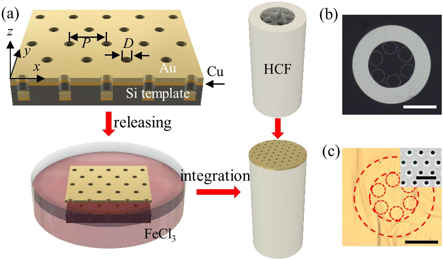
Fig. 1. (a) Schematic diagram of the fabrication process of the freestanding gold nanomembrane. Photographs of the (b) HCF and (c) freestanding gold nanomembrane on HCF. The dashed circles indicate the profile of the HCF beneath the gold nanomembrane. Scale bars, 50 μm; inset, SEM image of the gold nanomembrane (scale bar, 1 μm).
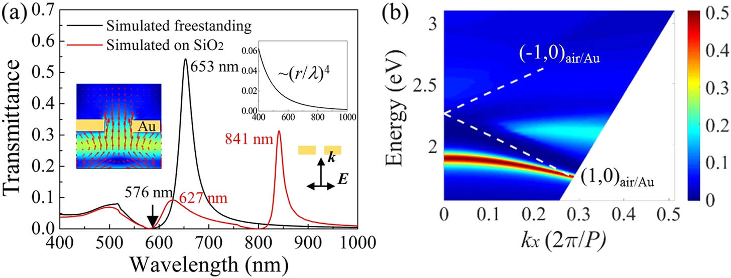
Fig. 2. (a) Simulated transmission spectra of the gold nanohole arrays with different configurations in air; insets, simulated electrical field | E | x − z
Fig. 3. (a) Simulated electrical field | E | x − y z | E z | 2 (a), respectively] in the x − z x = − 0.1 μm z | E | x − z SiO 2
Fig. 4. (a) Simulated transmission spectra of the gold nanohole arrays with different configurations in water; (b) calculated (dashed lines) and simulated (2D mapping) dispersion relations of the freestanding nanomembrane in water.
Fig. 5. (a) Simulated electrical field | E | z | E z | x − z x − y x = − 0.1 μm z 4 (a).
Fig. 6. Experimental (a) spectral evolution, (b) wavelength shifts and corresponding simulated (c) spectra, (d) wavelengths of the freestanding gold nanomembrane to varied refractive index. Experimental (e) spectral evolution, (f) wavelength shifts and corresponding simulated (g) spectra, (h) wavelengths of a gold nanomembrane on a solid silica fiber end face to varied refractive index.
Fig. 7. (a) Reflection spectra of the freestanding gold nanomembranes based on various configurations. The red dots and open circles indicate the corresponding resonance modes in experiments and simulations, respectively. (b) Evolution of the reflection spectra and (c) resonance wavelength shifts of the freestanding gold nanomembrane on the 125 μm hollow ferrule to varied refractive index; (d) simulated refractive index response of the freestanding gold nanomembrane.
|
Table 1. Comparison of Performances among Various Plasmonic Sensors Based on Nanohole Arrays

Set citation alerts for the article
Please enter your email address
© Copyright 2018-2021 | Chinese Laser Press. All Rights Reserved 沪ICP备15018463号-20