• Laser & Optoelectronics Progress
  • Vol. 55, Issue 1, 11101 (2018)
Liu Kangkang1, Meng Li1, Zhang Ning2、3、*, Sun Zhenwen2, Xie Bin3, Liu Xingxing3, and Xu Xiaojing2
Author Affiliations
  • 1School of Forensic Science, People''s Public Security University of China, Beijing 100038, China
  • 2National Engineering Laboratory for Forensic Science, Institute of Forensic Science, Ministry of Public Security,Beijing 100038, China
  • 3Public Security Bureau of Xingguo County, Ganzhou, Jiangxi 342400, China
  • show less
    DOI: 10.3788/LOP55.011101 Cite this Article Set citation alerts
    Liu Kangkang, Meng Li, Zhang Ning, Sun Zhenwen, Xie Bin, Liu Xingxing, Xu Xiaojing. Characterization of Electrical Tapes by Optical Coherence Tomography[J]. Laser & Optoelectronics Progress, 2018, 55(1): 11101 Copy Citation Text show less
    Photograph of electrical tape samples
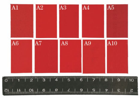
    Fig. 1. Photograph of electrical tape samples
    Photograph of frequency-domain OCT system
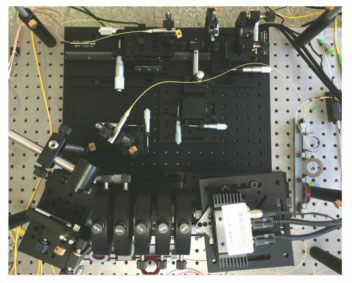
    Fig. 2. Photograph of frequency-domain OCT system
    Schematic of frequency-domain OCT system
    Fig. 3. Schematic of frequency-domain OCT system
    (a) 2D OCT cross-sectional image and (b) A-scan signal of an electrical tape
    Fig. 4. (a) 2D OCT cross-sectional image and (b) A-scan signal of an electrical tape
    (a) 2D OCT cross-sectional image of A1; (b) 2D OCT cross-sectional image of A2; (c) A-scan signal of A1; (d) A-scan signal of A2
    Fig. 5. (a) 2D OCT cross-sectional image of A1; (b) 2D OCT cross-sectional image of A2; (c) A-scan signal of A1; (d) A-scan signal of A2
    (a) 2D OCT cross-sectional image of A3; (b) 2D OCT cross-sectional image of A4; (c) A-scan signal of A3; (d) A-scan signal of A4
    Fig. 6. (a) 2D OCT cross-sectional image of A3; (b) 2D OCT cross-sectional image of A4; (c) A-scan signal of A3; (d) A-scan signal of A4
    (a) 2D OCT cross-sectional image of A5; (b) 2D OCT cross-sectional image of A6; (c) A-scan signal of A5; (d) A-scan signal of A6
    Fig. 7. (a) 2D OCT cross-sectional image of A5; (b) 2D OCT cross-sectional image of A6; (c) A-scan signal of A5; (d) A-scan signal of A6
    Fitted exponential curves of peak 1 and the following 10 points for samples (a) A7 and (b) A8
    Fig. 8. Fitted exponential curves of peak 1 and the following 10 points for samples (a) A7 and (b) A8
    (a) 3D reconstruction image of A9; (b) transverse sectional image of A9 at the depth of 100 μm; (c) 3D reconstruction image of A10; (d)transverse sectional image of A10 at the depth of 100 μm
    Fig. 9. (a) 3D reconstruction image of A9; (b) transverse sectional image of A9 at the depth of 100 μm; (c) 3D reconstruction image of A10; (d)transverse sectional image of A10 at the depth of 100 μm
    No.BrandManufacturer
    A1TESATESA, Germany
    A2COBRAHuaxia Industry Co., Ltd., Hebei, China
    A3YOUXINYouxin Packaging Materials Co., Ltd., Dongguan, China
    A4DELISino-American DELI Tools Co., Ltd., Yuyao, China
    A5SHUWANGShushi Industrial Co., Ltd., Hubei, China
    A6WANDEYahua Adhesive Product Co., Ltd., Tianjin, China
    A7VINIDenka Co., Ltd., Japan
    A8TIANTANTiantan Adhesive Product Co., Ltd., Beijing, China
    A9HUWANGHuaxia Industry Co., Ltd., Hebei, China
    A10SINCERESincere Adhesive Product Co., Ltd., Ningbo, China
    Table 1. Information of electrical tape samples
    No.Average optical path and error /μm
    A1162.96±1.68
    A2288.96±1.68
    A3297.36±1.68
    A4286.44±1.68
    A5288.12±2.06
    A6
    A7201.6±0
    A8177.24±3.14
    A9298.2±0
    A10274.68±2.06
    Table 2. Optical path of different electrical tape samples
    No.Average scattering intensity ratio and error
    A16.06±0.67
    A257.82±4.26
    A341.88±8.89
    A424.06±2.25
    A514.68±1.41
    A6
    A71.62±0.41
    A88.7±1.65
    A948.32±5.21
    A1016.18±1.86
    Table 3. Comparison of the scattering intensity ratio of different electrical tape samples
    No.Number of signal peaks
    A12
    A22
    A32
    A42
    A52
    A61
    A72
    A82
    A92
    A102
    Table 4. Number of signal peaks of different electrical tape samples
    No.Average attenuation coefficient and error
    A111.04±1.15
    A277.5±2.42
    A357.86±2.05
    A489.4±2.89
    A567.18±2.79
    A664.3±2.29
    A782.86±5.79
    A867.02±2.67
    A964.86±5.15
    A1058.38±2.08
    Table 5. Attenuation coefficients of different electrical tape samples
    A1A2A3A4A5A6A7A8A9
    A1
    A2a, b, d
    A3a, b, da, b, d
    A4a, b, da, b, da, b, d
    A5a, b, db, da, b, db, d
    A6c, dc, dc, dc, dc
    A7a, b, da, ba, b, da, ba, b, dc, d
    A8a, b, da, b, da, b, da, b, da, bca, b, d
    A9a, b, da, b, dda, b, da, bca, b, da, b
    A10a, b, da, b, da, ba, b, da, dc, da, b, da, b, da, b, d
    Table 6. Comparison of the significant difference (p<0.05) in the characteristic parameters of different samples
    Liu Kangkang, Meng Li, Zhang Ning, Sun Zhenwen, Xie Bin, Liu Xingxing, Xu Xiaojing. Characterization of Electrical Tapes by Optical Coherence Tomography[J]. Laser & Optoelectronics Progress, 2018, 55(1): 11101
    Download Citation