• Journal of Semiconductors
  • Vol. 42, Issue 5, 052101 (2021)
Li Zhang1, Haitao Qi1, Hongjuan Cheng1, Yuezeng Shi1, Zhanpin Lai1, and Muchang Luo2
Author Affiliations
  • 1China Electronics Technology Group Corp 46th Research Institute, Tianjin 300220, China
  • 2China Electronics Technology Group Corp 44th Research Institute, Chongqing 400060, China
  • show less
    DOI: 10.1088/1674-4926/42/5/052101 Cite this Article
    Li Zhang, Haitao Qi, Hongjuan Cheng, Yuezeng Shi, Zhanpin Lai, Muchang Luo. Morphology and crystalline property of an AlN single crystal grown on AlN seed[J]. Journal of Semiconductors, 2021, 42(5): 052101 Copy Citation Text show less
    (Color online) Surface topography of the AlN crystal grown at a seed surface temperature of 2200 °C. (a) Photograph. (b) Differential interference microscope. (c) SEM image.
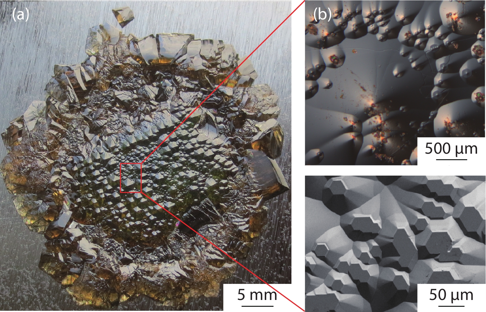
    Fig. 1. (Color online) Surface topography of the AlN crystal grown at a seed surface temperature of 2200 °C. (a) Photograph. (b) Differential interference microscope. (c) SEM image.
    (Color online) Surface topography of the AlN crystal grown at an increasing seed surface temperature of 2240 °C. (a) Photograph of the AlN crystal. (b) Differential interference microscope image in the center of the crystal. (c) Differential interference microscope image of terraces at the rim. (d) The AlN ingot after 20 h growth.
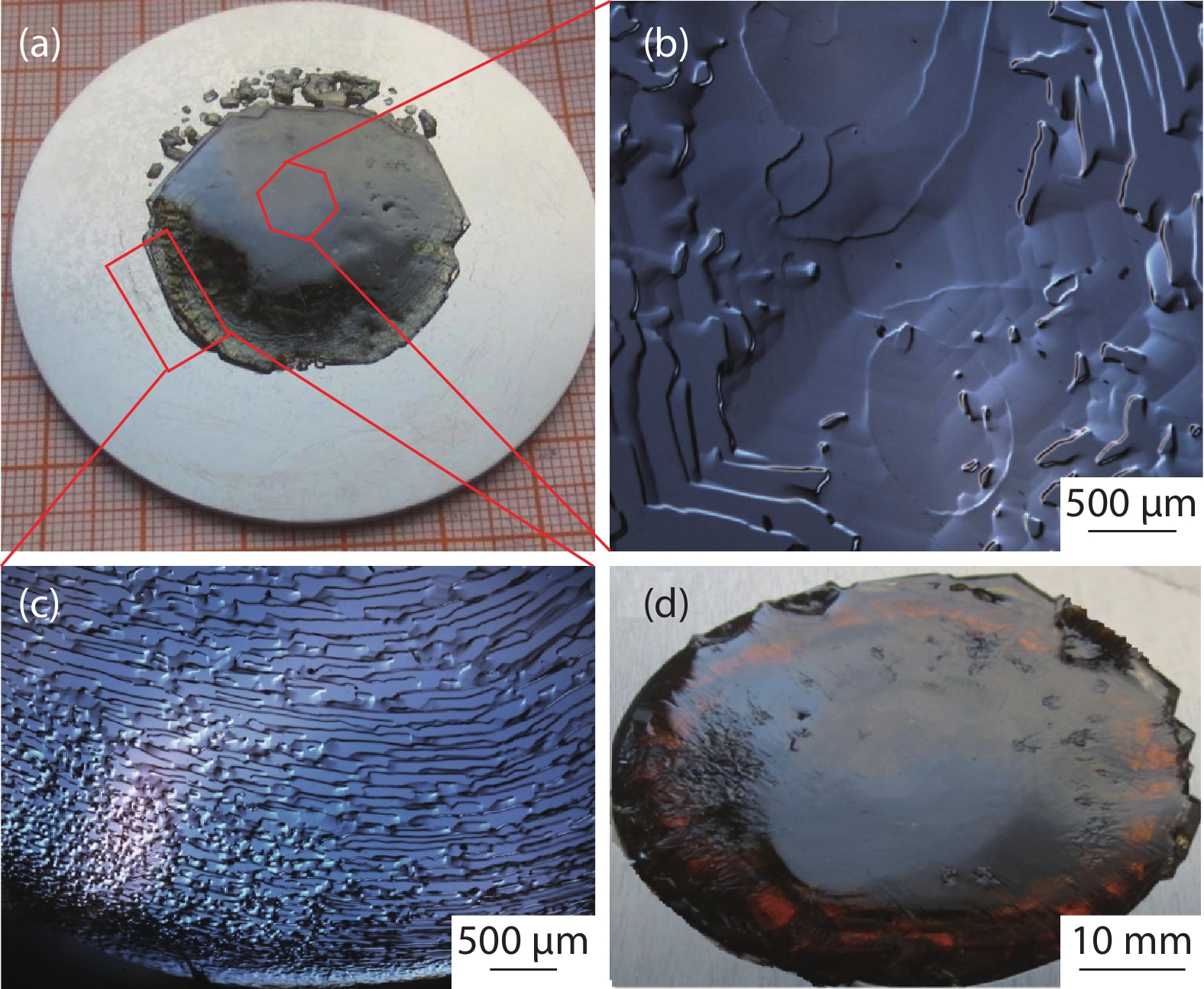
    Fig. 2. (Color online) Surface topography of the AlN crystal grown at an increasing seed surface temperature of 2240 °C. (a) Photograph of the AlN crystal. (b) Differential interference microscope image in the center of the crystal. (c) Differential interference microscope image of terraces at the rim. (d) The AlN ingot after 20 h growth.
    (Color online) The AlN crystal grown at optimized growth temperature of 2260 °C. Photograph of (a) the AlN crystal, (b) the AlN crystal grown after 24 h, and (c) the AlN ingot grown after 72 h.
    Fig. 3. (Color online) The AlN crystal grown at optimized growth temperature of 2260 °C. Photograph of (a) the AlN crystal, (b) the AlN crystal grown after 24 h, and (c) the AlN ingot grown after 72 h.
    (Color online) Crystallization properties of the AlN wafer. (a) 9 point Raman spectrums of the AlN crystal. (b) Mapping of 657 cm–1 Raman shifts. (c) HRXRD pattern of the AlN crystal with ω–2θ mode. (d) Rocking curve of (002) planes with Omega Rel scan mode. (e) Rocking curve of (102) planes with Omega Rel scan mode. (f) SEM image of etch pits.
    Fig. 4. (Color online) Crystallization properties of the AlN wafer. (a) 9 point Raman spectrums of the AlN crystal. (b) Mapping of 657 cm–1 Raman shifts. (c) HRXRD pattern of the AlN crystal with ω–2θ mode. (d) Rocking curve of (002) planes with Omega Rel scan mode. (e) Rocking curve of (102) planes with Omega Rel scan mode. (f) SEM image of etch pits.
    (Color online) (a) AlN polished wafer. (b) Surface roughness of the AlN polished wafer @ 10 × 10 μm2. (c) Schematic diagram of the epitaxial structure. (d) AFM of AlxGa1–xN epilayer. (e) HRXRD of AlxGa1–xN epilayer with ω–2θ scan mode. (f) High-resolution XRD reciprocal space mapping (RSM) of the (105) plane.
    Fig. 5. (Color online) (a) AlN polished wafer. (b) Surface roughness of the AlN polished wafer @ 10 × 10 μm2. (c) Schematic diagram of the epitaxial structure. (d) AFM of AlxGa1–xN epilayer. (e) HRXRD of AlxGa1–xN epilayer with ω–2θ scan mode. (f) High-resolution XRD reciprocal space mapping (RSM) of the (105) plane.
    AlN substrateAlN buffer layerAlxGa1–xN epitaxial layer
    (002)65 arcsec93 arcsec202 arcsec
    (102)36 arcsec29 arcsec496 arcsec
    Table 1. FWHMs of (002) and (102) reflection peaks in the substrate and epitaxial layer.
    Li Zhang, Haitao Qi, Hongjuan Cheng, Yuezeng Shi, Zhanpin Lai, Muchang Luo. Morphology and crystalline property of an AlN single crystal grown on AlN seed[J]. Journal of Semiconductors, 2021, 42(5): 052101
    Download Citation