• Journal of Semiconductors
  • Vol. 42, Issue 5, 052101 (2021)
Li Zhang1, Haitao Qi1, Hongjuan Cheng1, Yuezeng Shi1, Zhanpin Lai1, and Muchang Luo2
Author Affiliations
  • 1China Electronics Technology Group Corp 46th Research Institute, Tianjin 300220, China
  • 2China Electronics Technology Group Corp 44th Research Institute, Chongqing 400060, China
  • show less
    DOI: 10.1088/1674-4926/42/5/052101 Cite this Article
    Li Zhang, Haitao Qi, Hongjuan Cheng, Yuezeng Shi, Zhanpin Lai, Muchang Luo. Morphology and crystalline property of an AlN single crystal grown on AlN seed[J]. Journal of Semiconductors, 2021, 42(5): 052101 Copy Citation Text show less

    Abstract

    AlN single crystal grown by physical vapor transport (PVT) using homogeneous seed is considered as the most promising approach to obtain high-quality AlN boule. In this work, the morphology of AlN single crystals grown under different modes (3D islands and single spiral center) were investigated. It is proved that, within an optimized thermal distribution chamber system, the surface temperature of AlN seed plays an important role in crystal growth, revealing a direct relationship between growth mode and growth condition. Notably, a high-quality AlN crystal, with (002) and (102) reflection peaks of 65 and 36 arcsec at full width at half maximum (FWHM), was obtained grown under a single spiral center mode. And on which, a high-quality AlxGa1–xN epitaxial layer with high Al content (x = 0.54) was also obtained. The FWHMs of (002) and (102) reflection of AlxGa1–xN were 202 and 496 arcsec, respectively, which shows superiority over their counterpart grown on SiC or a sapphire substrate.

    1. Introduction

    An AlN single crystal has been considered as an optimum substrate for a III-nitride epitaxial layer due to its superior physical and chemical properties. And the application of AlN covers from deep ultraviolet detectors, deep ultraviolet LEDs to ultraviolet lasers as well as microwave high power devices[1]. However, it is difficult to grow an AlN single crystal from the melt phase due to its high melting point[2]. Among the approaches to obtain AlN bulk crystal, e.g., hydride vapor phase epitaxy (HVPE), physical vapor transport (PVT), metal organic chemical vapor deposition (MOCVD) and molecular bean epitaxy (MBE), PVT has gradually become the mainstream method owing to its high growth rate and with low dislocation density[3-10]. It should be noted that the seeds used for PVT growth often need to be a foreign substrate mismatched in a thermal expansion coefficient. Thus, the crystal quality of lateral grown AlN will deteriorate under each heating and cooling process within an imperfect thermal field. In order to obtain a high-quality AlN bulk crystal in inches, it is ideal to use a large area and high-quality homogeneous seed within one growth run. Dalmau and co-authors have announced an AlN seed diameter expansion from 36 to 47 mm with low dislocation density (<1000 cm–2) using the PVT method[11]. Hartmann et al. reports the newest results of homoepitaxial growth on an AlN single crystal substrate[12]. In addition to homogeneous AlN seed, which is expensive and difficult to obtain, another choice of PVT seed is an AlN/SiC heterostructure crystal. This heterostructure seed can be obtained by slicing the newly grown AlN crystal on the SiC seed[13-16]. Sumathi et al. uses 28 mm diameter free-standing AlN/SiC seed to prepare AlN crystals[13]. Chemekova et al. announced a 40 mm diameter AlN bulk with a thickness of ~1 cm by a two-stage technique of sublimation growth process, including seeding and initial growth of 2–3 mm thick single-crystal AlN layers on a 6H-SiC wafer[8]. However, these works shed light on the heterogeneous substrates. To our best of knowledge, the influence of initial morphology and growth mode is still lacking. We therefore, in this work, investigate the morphologies of AlN crystal grown under different conditions, and analyzed the relationship between the growth mode and the surface temperature of the seed. Besides, the crystalline properties were characterized using Raman spectrum and HRXRD. In addition, the obtained AlN boule was then sliced and polished into pieces to grow an AlxGa1–xN epilayer with a thickness of 500 nm using MOCVD.

    2. Experimental process

    An AlN bulk crystal growth experiment was carried out by PVT using a home-made resistance furnace. The resistance furnace, with sufficiently optimized thermal fields, was composed of tungsten heaters and multilayer tungsten shields. The AlN powder source used for vapor phase deposition was pre-sintered to eliminate any excess Al and oxygen components. Before the PVT experiment, GDMS measurement was conducted to ensure that the content of oxygen was below 10 ppm. Then the PVT process was carried out as follows: an AlN boule grown on the SiC seed, obtained according to our previous reported work[14], was sliced along [0001] direction into a plurality of pieces and polished mechano-chemically with surface roughness down to 0.5 nm before used as the starting seed. An AlN seed was fixed on a tungsten cap with its Al-polar face down towards the AlN powder source. The distance between the AlN seed and source was 50 mm. The temperature of the crucible bottom (measured using an infrared thermometer) and the pressure in the growth crucible were set to be 2350 °C and 700 mbar, respectively. In order to investigate the influence of growth mode on the morphology of grown AlN boules, the surface temperature of AlN seeds were set as 2200, 2240, and 2260 °C by adjusting the output of a top tungsten heater. For the growth of the AlxGa1–xN epilayer, a high-quality c-plane AlN seed prepared from spiral center growth mode was sliced and polished with a mean surface roughness (Ra) of ~0.097 nm. Then the AlxGa1–xN layer was deposited applying the MOCVD method by flowing TMA and TMG as Al and Ga sources as our previous work reported[17].

    An optical microscope and differential interference microscope (DICM) as well as a scanning electron microscope (SEM) were used to evaluate the morphology of the as-grown AlN boules. The crystalline quality was characterized by a high-resolution X-ray diffractometer (HRXRD, JV-DX) for both AlN boules and AlxGa1–xN epilayer. Raman spectroscopy (LabRAM HR800) was performed at room temperature using a 488 nm laser as excitation source, and the scanning wavelength was 200–1000 nm. High-resolution rocking curves were obtained by using a triple axis Bruker X-ray diffractometer equipped with a light source of Cu Kα1 X-ray. An AlN wafer was placed in a KOH/NaOH melt for 3 min and the dislocation density was counted by SEM. The quality of the homoepitaxially grown AlxGa1–xN epilayer was estimated by HRXRD, X-ray reciprocal space mapping (RSM) and an atomic force microscope (AFM).

    3. Results and discussion

    3.1. Surface morphology

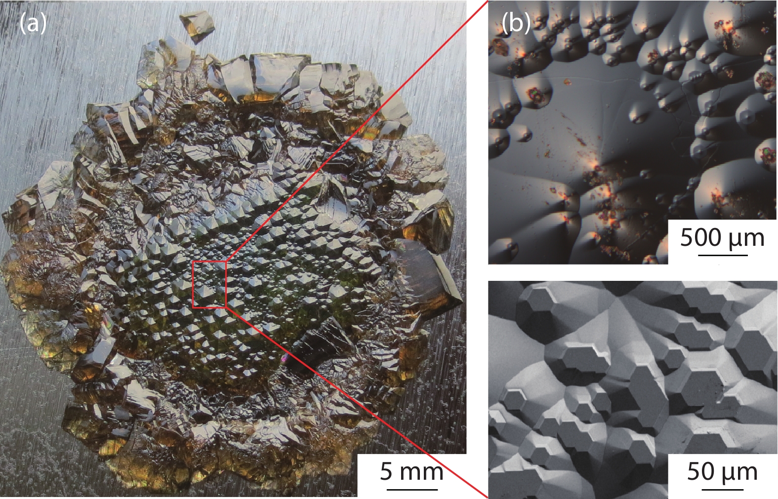
    With the purpose of revealing the relationship between growth mode and growth condition, the morphology of the as-prepared AlN crystal, grown under a relative low seed surface temperature of 2200 °C, was depicted in Fig. 1(a). The epitaxial crystals consist of a 100–500 μm pyramidal structure along the c direction on the main region and 1–5 mm irregular grains (mainly m plane) at the seed edge. According to reported references and our prior studies[14, 18], the emergence of m-plane grains relates to the excessive supersaturation of AlN vapor, which also was responsible for the higher rate of spontaneous nucleation than expansion growth of the AlN seed. It is known that the vapor transportation of the AlN gas species was driven by the temperature gradient (ΔT) in the furnace as given below:

    (Color online) Surface topography of the AlN crystal grown at a seed surface temperature of 2200 °C. (a) Photograph. (b) Differential interference microscope. (c) SEM image.

    Figure 1.(Color online) Surface topography of the AlN crystal grown at a seed surface temperature of 2200 °C. (a) Photograph. (b) Differential interference microscope. (c) SEM image.

    $ \Delta T=\frac{{T}_{2}-{T}_{1}}{d}, $ ()

    where is the temperature of the AlN powder source, is the surface temperature of the AlN seed, is the distance between the AlN source and seed. In the early stage of PVT, the quality of the as-grown crystal and its orientation depend on nucleation parameters, such as ΔT, partial pressure of AlN ( ), nucleation energy ( ) and supersaturation of AlN compounds on the seed surface ( ). Notably, with a constant and a well-established ΔT, is a decisive and facile controllable factor (by verifying the partial size of the AlN powder, pre-sintering status and fill ratio of the AlN source in crucible) that influences the morphology of AlN boules.

    For crystals grown on the AlN seed, as the amplified DICM image presented in Fig. 1(b), the morphology of the as-grown AlN crystal within the marked region is composed of a “primary” hexagonal pyramid with numerous surrounding “secondary” pyramids. We can also find that the primary pyramid grows perpendicularly on the initial Al-polar plane, while the secondary pyramids show a tilted angle of ~30° to the primary one, indicating a dominated growth towards c-axis with 3D islands. It is known that AlN gaseous segments are firstly driven to the seed interface by the axial temperature gradient ΔT, and then they nucleate at the seed surface. During this process, the quantities and orientations of nucleation are concerned with the nucleated energy, specifically the supersaturation in the seed interface. If the gas partial pressure keeps constant and axial temperature gradient ΔT is larger, the supersaturation required for crystal growth is more easily realized. Thereby, numerous AlN hexagonal pyramids are formed. In the sequent growth, the AlN gaseous are more easily nucleated at the top of pyramids formed as hexagon islands, as the SEM image shown in Fig. 1(c). However, the transverse expanded rate of pyramid islands are slow due to the low seed temperature and radial temperature gradient compared with an axial gradient, causing the tendency of axial growth. Some islands may merge into a bigger island. Some islands may develop lonely. So the growth surface still leaves lots of alone AlN islands after long time growth. So it can be inferred that the growth mode under seed surface temperature of 2200 °C[7] is a three-dimensional islands growth.

    After increasing the surface temperature of AlN seed from 2200 to 2240 °C, as shown in Fig. 2(a), a smooth topography with intrinsic plane of the { } was successfully obtained. We attribute this to a well-established thermal gradient, within which crystals growth along the c-axis was restricted. However, there are still some spontaneously nucleated polycrystalline grains observed on the tungsten holder and further growth optimization needs to be carried to realize the single-crystal AlN boule. In Fig. 2(b), we can find an isolated hexagonal-shaped nucleation center surrounded by numerous circular hexagonal steps. With an increased surface temperature of AlN seed, the axial temperature gradient and the supersaturation in crucible decrease. Thereby, the deposition rate of AlN vapor on seed or on tungsten surface decreases. This phenomenon reveals that, after increasing the growth rate along m-direction, the number of nucleation center decreases significantly. Moreover, as depicted in Fig. 2(c), macroscopic steps starting from regions with a growth spiral can be seen flowing smoothly in all directions. This kind of growth mode is normally observed while using slightly off-oriented (e.g. 2°) substrates[13], which also indicates a growth mode transformation from 3D islands to single spiral center.

    (Color online) Surface topography of the AlN crystal grown at an increasing seed surface temperature of 2240 °C. (a) Photograph of the AlN crystal. (b) Differential interference microscope image in the center of the crystal. (c) Differential interference microscope image of terraces at the rim. (d) The AlN ingot after 20 h growth.

    Figure 2.(Color online) Surface topography of the AlN crystal grown at an increasing seed surface temperature of 2240 °C. (a) Photograph of the AlN crystal. (b) Differential interference microscope image in the center of the crystal. (c) Differential interference microscope image of terraces at the rim. (d) The AlN ingot after 20 h growth.

    Then the as-prepared AlN was used as the seed to go another run (20 h) with furnace parameters unchanged. The lateral grown AlN crystal is presented in Fig. 2(d). A smooth surface with a { } intrinsic plane still exists. However, the growth core is gradually away from the center, which may be due to the irregular shape of the AlN source.

    A further optimized surface temperature from 2240 to 2260 °C was then used to grow the AlN crystal. The morphology of the AlN crystal is given in Fig. 3(a). The as-grown AlN surface with well-developed intrinsic { n} planes is smooth and there are not any poly-crystal grains on the periphery of the seed. This means that the growth temperature and supersaturation have been fully optimized. So, we carried out sequent growth using the as-obtained AlN as the seed. In Figs. 3(b) and 3(c), high-quality AlN crystals grown after 24 h and another 72 h are presented. The crystals are amber in color and have superior optical transmittance. The diameter and thickness of the AlN boule in Fig. 3(c) is 45 and 10 mm, respectively. Unfortunately, owing to the higher growth rate aroused by newly added AlN sources, there are some defects on this AlN boule.

    (Color online) The AlN crystal grown at optimized growth temperature of 2260 °C. Photograph of (a) the AlN crystal, (b) the AlN crystal grown after 24 h, and (c) the AlN ingot grown after 72 h.

    Figure 3.(Color online) The AlN crystal grown at optimized growth temperature of 2260 °C. Photograph of (a) the AlN crystal, (b) the AlN crystal grown after 24 h, and (c) the AlN ingot grown after 72 h.

    3.2. Crystallization quality

    The crystallization quality of the AlN wafer was characterized by means of measurement methods, as shown in Fig. 4. Before carrying out the characterizations, the AlN boule in Fig. 3(c) was sliced and polished into wafers. In Fig. 4(a), nine individual points were measured using Raman spectrum to evaluate the crystalline quality and uniformity of the obtained AlN wafer. Three peaks with the same wavenumbers of 247, 657 and 889 cm–1 can be seen in Raman results, corresponding to the phonon modes of E2 (low), E2 (high) and A1 (LO), respectively. These values are inconsistent with the modes of c-axis orientation AlN crystal[19]. Mapping of E2 (high) phonon mode peaks are shown in Fig. 4(b). The wavenumbers of E2 (high) phonon mode peaks ranges between 656.9 and 657.4 cm–1, these values are very close to stress-free peak of 657.4 cm–1[15, 16]. The center is almost stress-free, while the periphery of AlN wafer is suffering from tensile stress, which may be introduced during slicing and polishing processes. Notably, the coherent FWHM of Raman plots and the sharp E2 (high) phonon mode peaks with high-intensity indicate that the obtained AlN crystal has a good uniformity. The HRXRD pattern of the ω–2θ scan is represented in Fig. 4(c). Reflection peaks of (002) and (004), with diffraction angles at 36.02° and 76.42°, (102) at 49.97°, are in accordance with the standard values of Al bulk crystal. The equilibrium lattice parameters for the AlN wafer are calculated to be a = 3.113 Å and c = 4.982 Å. These crystal constants are in line with standard ones, demonstrating an extremely low deformation existing in our AlN boule. The symmetric (002) and asymmetric (102) X-ray diffraction rocking curves are shown in Figs. 4(d) and 4(e), respectively. Both of the peaks for (002) and (102) reflection are narrow, and the FWHMs of the curves are 65 and 36 arcsec, respectively. These values are slightly higher than the best record of 13 arcsec in the latest report[20], but much better than our previous work of 120 arcsec[14]. Fig. 4(f) shows the SEM image of etch pits of the AlN wafer. The main type of etch pit is screw dislocation with a large size, and the total etch pit density (EPD) is 5 × 105 cm–2.

    (Color online) Crystallization properties of the AlN wafer. (a) 9 point Raman spectrums of the AlN crystal. (b) Mapping of 657 cm–1 Raman shifts. (c) HRXRD pattern of the AlN crystal with ω–2θ mode. (d) Rocking curve of (002) planes with Omega Rel scan mode. (e) Rocking curve of (102) planes with Omega Rel scan mode. (f) SEM image of etch pits.

    Figure 4.(Color online) Crystallization properties of the AlN wafer. (a) 9 point Raman spectrums of the AlN crystal. (b) Mapping of 657 cm–1 Raman shifts. (c) HRXRD pattern of the AlN crystal with ω–2θ mode. (d) Rocking curve of (002) planes with Omega Rel scan mode. (e) Rocking curve of (102) planes with Omega Rel scan mode. (f) SEM image of etch pits.

    An AlN polished wafer with the size of 10 × 10 mm2 and a thickness of 500 μm shown in Fig. 5(a) was used as the substrate for further epitaxial growth. The surface of the polished AlN wafer is smooth and the surface roughness (Ra) is 0.097 nm, as shown in Fig. 5(b). An AlxGa1–xN epitaxial layer was grown on the AlN substrate by the MOCVD method and the structure of epitaxial layers is shown in Fig. 5(c). Before depositing the AlxGa1–xN layer, a 500 nm AlN epitaxial layer was deposited on the AlN substrate as a buffer layer. The AFM image with a scan range of 10 × 10 μm2 of the as-fabricated AlxGa1–xN epitaxial layer is shown in Fig. 5(d). The smooth surface with atomic steps is clearly seen, which demonstrates the superiority of homogeneous epitaxy on the AlN substrate. Rocking curve FWHMs of (002) symmetric and (102) asymmetric reflection peaks of AlxGa1–xN epitaxial are shown in Table 1. It should be noted here that the FWHM of (102) reflection peak of AlxGa1–xN epitaxial layer is less than 500 arcsec, indicating a lower dislocation density compared with that on the sapphire substrate.

    (Color online) (a) AlN polished wafer. (b) Surface roughness of the AlN polished wafer @ 10 × 10 μm2. (c) Schematic diagram of the epitaxial structure. (d) AFM of AlxGa1–xN epilayer. (e) HRXRD of AlxGa1–xN epilayer with ω–2θ scan mode. (f) High-resolution XRD reciprocal space mapping (RSM) of the (105) plane.

    Figure 5.(Color online) (a) AlN polished wafer. (b) Surface roughness of the AlN polished wafer @ 10 × 10 μm2. (c) Schematic diagram of the epitaxial structure. (d) AFM of AlxGa1–xN epilayer. (e) HRXRD of AlxGa1–xN epilayer with ω–2θ scan mode. (f) High-resolution XRD reciprocal space mapping (RSM) of the (105) plane.

    Table Infomation Is Not Enable

    The HRXRD results given in Fig. 5(e) was obtained using ω–2θ scan mode. The left peak at 17.6° relates to the AlxGa1–xN epitaxial layer, while the right peak at 18.0°, stands for the AlN epitaxial layer or the AlN substrate. Eventually, the Al content x is derived to be 0.54 from a cubic equation according to a reported work[21]. Moreover, the X-ray RSM of the (105) plane is shown in Fig. 5(f), and the relaxation of Al0.54Ga0.46N epitaxial layer can be calculated by the following formulas:

    $ {f}_{\perp }=\frac{{K}_{\rm s\perp }-{K}_{\rm l\perp }}{{K}_{\rm l\perp }}, $ ()

    $ {f}_{//}=\frac{{K}_{\rm s//}-{K}_{\rm l//}}{{K}_{\rm l//}}, $ ()

    $ f=\left({f}_{\perp }-{f}_{//}\right)\frac{1-v}{1+v}+{f}_{//}, $ ()

    $ R=\frac{{f}_{//}}{f}, $ ()

    where is the crystal lattice mismatch, and // is perpendicular and parallel direction, respectively, s and l represent substrate and layer, respectively, v is passion ratio, = 0.25, = 0.203, then = 0.228. The calculated relaxation R of Al0.54Ga0.46N epitaxial layer is 44.8%, demonstrating that this 500 nm thick high Al content AlxGa1–xN epitaxial layer is still not fully relaxed. As we know, a large number of structural defects, cracks and stress relaxation in the AlxGa1–xN epitaxial layer would be induced if there is a lattice mismatch and thermal mismatch between the epitaxial layer and the substrate (such as sapphire or SiC substrate or GaN template). So, it can be deduced that the high-quality AlxGa1–xN epitaxial layer has been grown on the AlN single crystal, which further indicates the superiority of homogeneous growth on the AlN substrate.

    4. Conclusion

    We demonstrate in this work a high-quality AlN boule grown using the PVT method. The relationship between surface morphology and growth mode was investigated by comparing the as-grown AlN crystals under different growth conditions. Briefly, the AlN crystal grown under a lower seed temperature has a higher temperature gradient along c-axial, resulting in a rough surface and hexagonal pyramids grown in a dislocation-modulated 3D islands growth mode. After increasing the seed temperature, the growth mode changes to single spiral growth mode. And the as-grown AlN crystal has a smooth surface, hexagonal nucleation center and intrinsic { n} planes. Then an amber AlN single crystal with well-developed { n} intrinsic plane was successfully obtained by further optimizing the thermal field of the furnace and increasing the seed temperature. The FWHMs of (002) and (102) reflection peaks of the AlN wafer is 65 and 36 arcsec, respectively. The surface roughness of the polished AlN is 0.097 nm, making it an appropriate substrate for the epitaxial growth of the AlxGa1–xN layer. The Al content and the relaxation of the as-prepared AlxGa1–xN epilayer are calculated to be 0.54 and 44.8%, respectively. The FWHMs of (002) and (102) reflection AlxGa1–xN epilayer is 202 and 496 arcsec, respectively.

    Acknowledgements

    This work was supported by the National Key Research and Development Plan of China (2017YFB0404103) and the National Natural Science Foundation of China (No.51702297).

    References

    [1] C Hartmann, A Dittmar, J Wollweber et al. Bulk AlN growth by physical vapour transport. Semicond Sci Technol, 29, 084002(2014).

    [2] O Filip, B M Epelbaum, M Bickermann et al. Effects of growth direction and polarity on bulk aluminum nitride crystal properties. J Cryst Growth, 318, 427(2011).

    [3] G A Slack, T F McNelly. Growth of high purity AlN crystals. J Cryst Growth, 34, 263(1976).

    [4] E Mokhov, I Izmaylova, O Kazarova et al. Specific features of sublimation growth of bulk AlN crystals on SiC wafers. Phys Status Solidi C, 10, 445(2013).

    [5] M Bickermann, O Filip, B M Epelbaum et al. Growth of AlN bulk crystals on SiC seeds: Chemical analysis and crystal properties. J Cryst Growth, 339, 13(2012).

    [6] I Nagai, T Kato, T Miura et al. AlN bulk single crystal growth on 6H-SiC substrates by sublimation method. J Cryst Growth, 312, 2699(2010).

    [7] C Hartmann, M Albrecht, J Wollweber et al. SiC seed polarity-dependent bulk AlN growth under the influence of residual oxygen. J Cryst Growth, 344, 19(2012).

    [8] T Y Chemekova, O V Avdeev, I S Barash et al. Sublimation growth of 2 inch diameter bulk AlN crystals. Phys Status Solidi C, 5, 1612(2008).

    [9] M Bickermann, B M Epelbaum, O Filip et al. Faceting in AlN bulk crystal growth and its impact on optical properties of the crystals. Phys Status Solidi C, 9, 449(2012).

    [10] R R Sumathi, R U Barz, T Straubinger et al. Structural and surface topography analysis of AlN single crystals grown on 6H-SiC substrates. J Cryst Growth, 360, 193(2012).

    [11] R Dalmau, H S Craft, J Britt et al. High quality AlN single crystal substrates for AlGaN-based devices. Mater Sci Forum, 924, 923(2018).

    [12] C Hartmann, L Matiwe, J Wollweber et al. Favourable growth conditions for the preparation of bulk AlN single crystals by PVT. CrystEngComm, 22, 1762(2020).

    [13] R R Sumathi. Bulk AlN single crystal growth on foreign substrate and preparation of free-standing native seeds. CrystEngComm, 15, 2232(2013).

    [14] L Zhang, H T Qi, H J Cheng et al. Preparation and characterization of AlN seeds for homogeneous growth. J Semicond, 40, 102801(2019).

    [15] M Bickermann, B M Epelbaum, O Filip et al. Deep-UV transparent bulk single-crystalline AlN substrates. Phys Status Solidi C, 7, 1743(2010).

    [16] M Bickermann, B M Epelbaum, O Filip et al. UV transparent single-crystalline bulk AlN substrates. Phys Status Solidi C, 7, 21(2010).

    [17] W X Yang, Y K Zhao, Y Y Wu et al. Deep-UV emission at 260 nm from MBE-grown AlGaN/AlN quantum-well structures. J Cryst Growth, 512, 213(2019).

    [18] M Bobea Graziano, I Bryan, Z Bryan et al. Structural characteristics of m-plane AlN substrates and homoepitaxial films. J Cryst Growth, 507, 389(2019).

    [19] W Zheng, R S Zheng, F Huang et al. Raman tensor of AlN bulk single crystal. Photon Res, 3, 38(2015).

    [20] P Lu, R Collazo, R F Dalmau et al. Seeded growth of AlN bulk crystals in m- and c-orientation. J Cryst Growth, 312, 58(2009).

    [21] K Jiang, X J Sun, J W Ben et al. Suppressing the compositional non-uniformity of AlGaN grown on a HVPE-AlN template with large macro-steps. CrystEngComm, 21, 4864(2019).

    Li Zhang, Haitao Qi, Hongjuan Cheng, Yuezeng Shi, Zhanpin Lai, Muchang Luo. Morphology and crystalline property of an AlN single crystal grown on AlN seed[J]. Journal of Semiconductors, 2021, 42(5): 052101
    Download Citation