• Journal of Semiconductors
  • Vol. 44, Issue 4, 042802 (2023)
Ashish Kumar1、2、*, Jayjit Mukherjee3, D. S. Rawal3, K. Asokan2, and D. Kanjilal2
Author Affiliations
  • 1Department of Physics, School of Natural Science, University of Petroleum and Energy Studies, Bidholi, Dehradun - 248007, India
  • 2Inter University Accelerator Centre, Aruna Asaf Ali Road, Vasantkunj, New Delhi - 110067, India
  • 3Solid State Physics Laboratory, DRDO, Timarpur, New Delhi - 110054, India
  • show less
    DOI: 10.1088/1674-4926/44/4/042802 Cite this Article
    Ashish Kumar, Jayjit Mukherjee, D. S. Rawal, K. Asokan, D. Kanjilal. Trap analysis on Pt-AlGaN/GaN Schottky barrier diode through deep level transient spectroscopy[J]. Journal of Semiconductors, 2023, 44(4): 042802 Copy Citation Text show less
    (Color online) Schematic of the Pt-AlGaN/GaN SBD under experimentation.
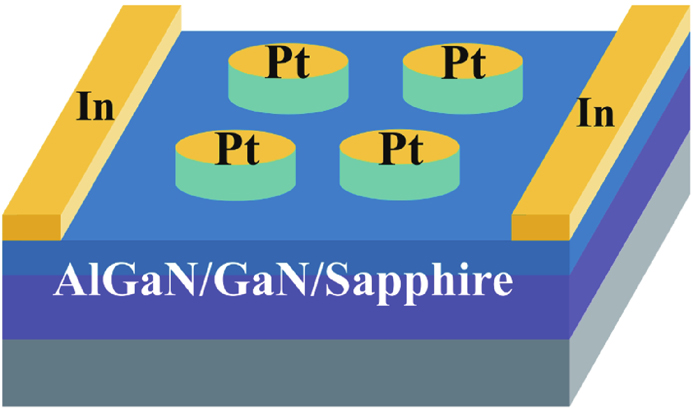
    Fig. 1. (Color online) Schematic of the Pt-AlGaN/GaN SBD under experimentation.
    (Color online) DLTS setup used for the experimentation.
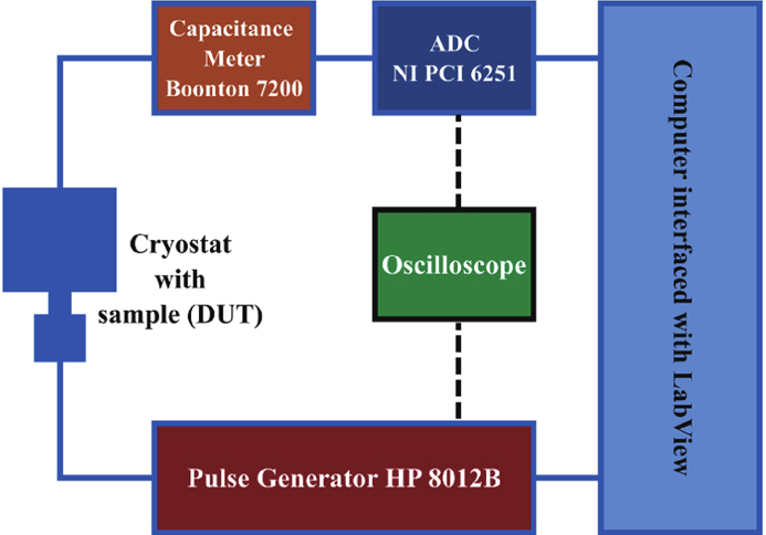
    Fig. 2. (Color online) DLTS setup used for the experimentation.
    (Color online) (a) DLTS signal for r = 2 with t1 ranging from 10–150 ms. The vertical dashed lines are the peak position as they appear in the spectra for the first instance of sampling time. The inset shows the gaussian fit with the experimental data. (b) Calculated activation energies for the two peaks as denoted by P12and P22.
    Fig. 3. (Color online) (a) DLTS signal for r = 2 with t1 ranging from 10–150 ms. The vertical dashed lines are the peak position as they appear in the spectra for the first instance of sampling time. The inset shows the gaussian fit with the experimental data. (b) Calculated activation energies for the two peaks as denoted by P12 and P22 .
    (Color online) (a) DLTS signal for r = 3 with t1 ranging from 10–200 ms. The vertical dashed lines are the peak position as they appear in the spectra for the first instance of sampling time. The inset shows the fit with the experimental data. (b) Calculated activation energies for trap peaks P13, P23, and P33.
    Fig. 4. (Color online) (a) DLTS signal for r = 3 with t1 ranging from 10–200 ms. The vertical dashed lines are the peak position as they appear in the spectra for the first instance of sampling time. The inset shows the fit with the experimental data. (b) Calculated activation energies for trap peaks P13 , P23 , and P33 .
    (Color online) (a) DLTS signal for r = 5 for t1 = 10–150 ms. The vertical dashed lines are the peak position as they appear in the spectra for the first instance of sampling time. The inset shows the fit with the experimental data. (b) Calculated activation energies for the trap peaks for r = 5 and r = 10.
    Fig. 5. (Color online) (a) DLTS signal for r = 5 for t1 = 10–150 ms. The vertical dashed lines are the peak position as they appear in the spectra for the first instance of sampling time. The inset shows the fit with the experimental data. (b) Calculated activation energies for the trap peaks for r = 5 and r = 10.
    (Color online) Trap energy levels from DLTS for different ratios of the rate windows. The energy level corresponds to the offset from conduction band edge (EC) for electron traps and from valence band edge (EV) for hole traps.
    Fig. 6. (Color online) Trap energy levels from DLTS for different ratios of the rate windows. The energy level corresponds to the offset from conduction band edge (EC) for electron traps and from valence band edge (EV) for hole traps.
    Ratio (r)Trap peak, natureEa (eV)NT (1016 cm−3)RemarkRef.
    *This trap level was also evident after e/ γ -irradiation on GaN SBDs.
    2P12 , eEC – 0.872.05Nitrogen interstitial (Ni)[2931]
    P22 , hEV + 1.561.03
    3P13 , eEC – 0.055.14Open core dislocation[32,35]
    P23 , eEC – 1.003.08Threading dislocations[34]
    P33 , hEV + 1.371.17AlGaN/GaN interface[35,36]
    5P15 , eEC – 0.094.41Nitrogen vacancies[37,38,41]*
    P25 , eEC – 1.213.23Extended defects in GaN[35,36]
    P35 , hEV + 2.291.54Ga-vacancy/N-antisite[44]
    10P110 , eEC – 0.172.82Bulk GaN/interface states[45,46]
    P210 , eEC – 1.222.79Extended defects in GaN[35,36]
    P310 , hEV + 2.661.45Point/extended defects[47]
    Table 1. Summary of the electron and hole traps from the DLTS experimentation. Ea is the activation energy of the trap measured from the conduction (EC) or valence band (wV) edge, and NT is the trap density as calculated from the Arrhenius plots.
    Ashish Kumar, Jayjit Mukherjee, D. S. Rawal, K. Asokan, D. Kanjilal. Trap analysis on Pt-AlGaN/GaN Schottky barrier diode through deep level transient spectroscopy[J]. Journal of Semiconductors, 2023, 44(4): 042802
    Download Citation