Ashish Kumar, Jayjit Mukherjee, D. S. Rawal, K. Asokan, D. Kanjilal. Trap analysis on Pt-AlGaN/GaN Schottky barrier diode through deep level transient spectroscopy[J]. Journal of Semiconductors, 2023, 44(4): 042802
Copy Citation Text
Trap characterization on GaN Schottky barrier diodes (SBDs) has been carried out using deep-level transient spectroscopy (DLTS). Selective probing by varying the ratio of the rate window values (r) incites different trap signatures at similar temperature regimes. Electron traps are found to be within the values: 0.05–1.2 eV from the conduction band edge whereas the hole traps 1.37–2.66 eV from the valence band edge on the SBDs. In the lower temperature regime, the deeper electron traps contribute to the capacitance transients with increasing r values, whereas at the higher temperatures >300 K, a slow variation of the trap levels (both electrons and holes) is observed when r is varied. These traps are found to be mainly contributed to dislocations, interfaces, and vacancies within the structure.Trap characterization on GaN Schottky barrier diodes (SBDs) has been carried out using deep-level transient spectroscopy (DLTS). Selective probing by varying the ratio of the rate window values (r) incites different trap signatures at similar temperature regimes. Electron traps are found to be within the values: 0.05–1.2 eV from the conduction band edge whereas the hole traps 1.37–2.66 eV from the valence band edge on the SBDs. In the lower temperature regime, the deeper electron traps contribute to the capacitance transients with increasing r values, whereas at the higher temperatures >300 K, a slow variation of the trap levels (both electrons and holes) is observed when r is varied. These traps are found to be mainly contributed to dislocations, interfaces, and vacancies within the structure.
Introduction
Gallium nitride has proved to be a superior material due to its advanced qualities like high bandgap and high thermal conductivity[1,2]. These advantages over other conventional semiconductors have led GaN to be used in multiple applications in power electronic devices, optoelectronics as in LEDs, LASERs, photo-detectors, and solar cells[3-6]. The AlGaN/GaN heterojunction with inherent interface polarization leads to high mobilities and high saturation velocities in 2D electron gas (2DEG) at interface and is most suitable for high-frequency applications. Despite all the above application advantages, GaN systems also face reliability issues due to the presence of defects/traps within the epitaxial layers and at the interfaces[7,8].
The heterostructure used for devices fabrication plays a crucial role in governing the device characteristics. Epitaxial growth on lattice-mismatched substrates leads to tensile and compressive strains which lead to dislocations and extended defects. Furthermore, the AlGaN/GaN interface may also house interface states which readily modulate the 2DEG concentration at the interface and results in degraded device performance. Micro and optoelectronic devices require a defect-free surface, an active layer immune to any dislocation/defect beneath it, and a good crystalline quality material. It is reported that the charge imbalance caused due to carrier trapping by defects leads to high leakage currents[9], breakdown[10], current collapse in HEMTs[11], and reduced quantum efficiency in light-emitting diodes[12]. The aforementioned material superiority of GaN has led to widespread research for power applications. A vast of the reported work has utilized a Ni-based metal scheme for the gate contact[13-18]. However, the leakage in the devices can be improved by using higher work function metals for the gate contact. Pt having a work function of 5.65 eV[19] has been reported having a higher barrier height[20] as compared to conventional Ni/Au gate contacts on GaN-based devices. Enhanced barrier height has also been achieved through annealing of the Schottky contact[21-23]. Apart from conventional nitride passivation, the surface states can also be mitigated through Ru or sulphide-based schemes[24,25]. Thereby characterization of these defects is important towards the development of reliable GaN devices. Detailed trap signature studies of GaN with Pt-Schottky contacts are not available in the reported literature and needs to be studied using reliable technique for stable GaN device operation in power/RF electronics. Deep level transient spectroscopy (DLTS)[26] offers substantial advantages over other characterization techniques[23,27,28] to study deep trap states which are not easily obtained from other conventional methods.
In this article, we have analyzed Pt-AlGaN/GaN Schottky barrier diode (SBD) on sapphire using deep level transient spectroscopy (DLTS) throughout a temperature range of 150–480 K. The variation of the ratio of the rate windows reveals numerous trap signatures within the device throughout the observed temperature range and enables selective probing of deep traps present within the epitaxial layers. A higher temperature regime has been probed for the wide band gap material and the findings provide all the possible trap signatures that may be introduced into GaN systems which can have detrimental impact on device performance. This helps to expand the understanding of the traps originating from extended defects and interface states and how traps respond in different temperature regimes.
Experimental details
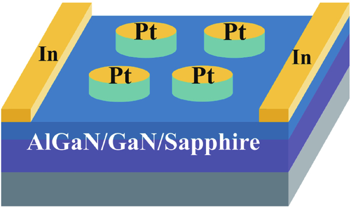
The SBDs were fabricated on commercially procured AlGaN/GaN heterostructure grown on the sapphire substrate by metal-organic chemical vapor deposition (MOCVD) technique. Circular platinum (Pt) dots (1.5 mm diameter, 100 nm thickness) were deposited using a metal mask in an ultra-high vacuum chamber followed by Indium (In) metal strips deposited at opposite edges for ohmic contacts as shown in the schematic diagram inFig. 1. DLTS characterization was done by a conventional boxcar method comprised of a capacitance meter (Boonton 7200), a pulse generator (HP 8012B), temperature controller (Lakeshore 340), ADC digitizer (DAQ card NI PCI 6251), and a computer interfaced with LabVIEW software. A temperature range of 150–480 K was used for the DLTS spectrum with a voltage excitation of 10 V (square pulse) applied on the SBD. The setup of the DLTS instrumentation is schematically shown inFig. 2. The filling and emptying pulse-width were kept at 2 and 10 ms respectively with a pulse sampling rate of 50 ms. The DLTS signal was captured by sampling capacitance transient data at different time intervals in the range of 5 μs to 9 ms. As demonstrated by Lang[26], the DLTS signal is generated from the difference in the C(t) spectrum (Eq. (1)) for two sampling times (t1 and t2) defined by a rate window (t1 – t2) utilizing a double boxcar integrator.
Figure 1.(Color online) Schematic of the Pt-AlGaN/GaN SBD under experimentation.
Here,
is the zero-bias capacitance,
is the trap concentration, and
is the donor concentration. When the temperature (T) is varied, the time constant (
) corresponding to a particular trap changes, this leads to a maximum in the DLTS signal as obtained from the capacitance transients. For different sampling times (rate windows), a specific value of
is obtained (Eq. (2)). These values are used to generate the Arrhenius plot following Eq. (3), from which the trap activation energy (
) can be calculated.
where
is the Boltzmann constant,
is the trap concentration,
with
as the thermal velocity and
as the effective density of states. The DLTS analysis results have been presented for four rate windows ratios r = t2/t1 (= 2, 3, 5 and 10) to get the maximum number of trap signatures in the SBDs. For the analysis, we have chosen the positive peaks in the DLTS signal for the electron traps as per the convention (which was preset from the experimental setup). The DLTS spectra is a result of multiple trap signatures (since any change in trap occupancy is directly reflected in the capacitance), hence multiple peaks correspond to multiple traps. Thus, the peaks were deconvoluted and analyzed with gaussian fitting function to determine the peak positions for a particular trap.
Results and discussion
The DLTS spectra for r = 2 are presented in Fig. 3(a) for different t1 values between (10–150 ms). A positive peak
at around 330 K for high t1 values and for 10 ms is observed. Along with it, a negative peak
around 400 K is also observed for high t1 values. The activation energies calculated from the Arrhenius plots are shown inFig. 3(b). The
peak corresponds to an electron trap EC – 0.87 eV and the
extracts a hole trap of EV + 1.56 eV. The electron trap peak
decreases with increasing t1 values whereas the hole trap peak
appears for t1 = 50 ms and remains constant till 250 ms. A similar deep-level electron trap in GaN (
) has been ascribed to nitrogen interstitials (Ni) and observed in low C-doped SBDs and high quality GaN films. Various studies have also shown yellow luminescence in GaN originating from trap centres with similar activation energies (0.75 to 0.89 eV)[29-31].
Figure 3.(Color online) (a) DLTS signal for r = 2 with t1 ranging from 10–150 ms. The vertical dashed lines are the peak position as they appear in the spectra for the first instance of sampling time. The inset shows the gaussian fit with the experimental data. (b) Calculated activation energies for the two peaks as denoted by
and
.
Next,Fig. 4 shows DLTS analysis for rate window ratio r = 3, where three traps are evident: two-electron traps
,
, and a hole trap
. All the evident traps are identified for t1 values \gt 50 ms and the peaks gradually decrease for t1 = 200 ms shown inFig. 4. The trap peak
is a shallow level around 0.05 eV from the conduction band edge. In contrast to other traps evaluated with this rate window, the trap peak moves towards lower temperatures with increasing t1. Shallow trap levels around EC – 0.04 eV originate due to open core dislocations within the crystal structure[32,33]. The
is a deep trap with an activation energy of 1 eV. This trap was also evident from DLTS on GaN-based SBDs with thin GaN layers and are generally associated with threading dislocations[34]. The hole trap
with the energy level of EV + 1.37 eV peaks around 400 K. Deep hole traps similar to
have been previously reported to be present in the AlGaN/GaN heterointerface from DLTS studies[35,36] and the same is to be accounted in this experiment as the SBDs are fabricated on AlGaN/GaN heterostructure.
Table Infomation Is Not Enable
Figure 4.(Color online) (a) DLTS signal for r = 3 with t1 ranging from 10–200 ms. The vertical dashed lines are the peak position as they appear in the spectra for the first instance of sampling time. The inset shows the fit with the experimental data. (b) Calculated activation energies for trap peaks
,
, and
.
The rate window r = 5 reveals three trap levels (Fig. 5(a)) with one shallow electron peak (
), a deep electron peak (
), and a deep hole peak (
). The
trap of EC – 0.09 eV has been reported as a native defect in n-GaN due to nitrogen vacancies (VN) leading to shallow levels around 100 meV[37]. Apart from pristine GaN SBDs, a similar trap level was reported in n-GaN SBDs after undergoing cumulative doses of 60Co-
-radiation[38]. The heavy ion irradiation on GaN SBDs facilitates defect formation as reported in Refs. [39,40]. The defects have been explained to be generated from N vacancies when energetic radiation/electrons on collision with GaN surface create either VN–NI Frenkel pairs and/or defects composed of longer chains[41,42]. Deep electron trap like
around 1.2 eV has been correlated to extended defects in bulk GaN[35] as well as electron-irradiated SBDs[43]. A deep hole trap,
= EV + 2.29 eV peaking around 400 K is also observed. The spectrally resolved measurement reveals a trap centered around 2.27 eV from the valence band edge (EV)[44] possibly from gallium vacancy (VGa) or nitrogen antisite (NGa). This trap is found to be responsible for optical quenching-related anomalous dispersion of off-state leakage current under illumination in GaN HEMT.
Figure 5.(Color online) (a) DLTS signal for r = 5 for t1 = 10–150 ms. The vertical dashed lines are the peak position as they appear in the spectra for the first instance of sampling time. The inset shows the fit with the experimental data. (b) Calculated activation energies for the trap peaks for r = 5 and r = 10.
Higher ratios lead to deeper trap states being resolved through DLTS as shown inFig. 5(b). We observed a shallow electron trap
of 0.17 eV which has been discussed in Refs. [45,46] reportedly around EC – 0.18 eV, originates from bulk GaN and/or interface states in AlGaN/GaN HEMTs. The
electron trap exactly reciprocates the
trap as obtained earlier centered around 325 K. The deep hole trap
has an energy level of EV + 2.66 eV. This is also consistent with Armstrong[47] who has reported a high-density deep hole trap around 2.59 eV from valence band edge for InGaN/GaN heterostructures from deep level optical spectroscopy (DLOS) studies. They ascribed this to most likely point or extended defects in InGaN underlayers. The summary of all the trap states as extracted from the DLTS analysis is presented inTable 1 along with the trap properties.
From the trap signatures as a result of extensive experimentation, it is evident that by increasing the ratio (r) of the rate windows (t1, t2) different traps corresponding to similar temperature regimes were evaluated as shown inFig. 6. For this, we focus on the three most dominant trap peaks as evident in the DLTS spectra for different r-values. The temperature range is divided into three regions. Region I (<250 K) is predominantly characterized by shallow electron traps and an increase in the trap energy level is observed as r is increased. It is also interesting to note that for all the evaluated shallow levels for different rate windows (
and
), the DLTS peaks shift to lower temperatures with increasing t1 values. This leads to obtaining shallow electron traps in a lower temperature regime with different dynamics as compared to the other deep levels. The trap peaks in region II (300–350 K) correspond to deep traps and become invariant revealing a constant electron trap of EC – 1.2 eV for r = 5 and 10. The hole trap peaks observed in region III (around 400 K) show a non-monotonic increase in energy values with 2.66 eV for r = 10. The higher r-value helps to find traps with larger time constants and thereby deep trap states within the heterostructure, which is evident from the traps in regions I and III. This leads to the selective probing of traps being evident in different temperature regimes.
Figure 6.(Color online) Trap energy levels from DLTS for different ratios of the rate windows. The energy level corresponds to the offset from conduction band edge (EC) for electron traps and from valence band edge (EV) for hole traps.
Present investigation on Pt-AlGaN/GaN SBDs through DLTS has revealed various electron and hole trap levels. In the analysis, the number of trap peaks observed also changes with the r value with higher r-values revealing a greater number of trap peaks. It was also observed that traps originating from different defect centers respond in similar temperature regimes. This can be used for selective probing of electron and hole traps. The trap levels are compared to those reported earlier which are attributed to dislocations, AlGaN/GaN interface, and vacancy defects within the epitaxial layers. The above results from this extensive DLTS experimentation reveal a wide view of the trap signatures in GaN systems.
Ashish Kumar, Jayjit Mukherjee, D. S. Rawal, K. Asokan, D. Kanjilal. Trap analysis on Pt-AlGaN/GaN Schottky barrier diode through deep level transient spectroscopy[J]. Journal of Semiconductors, 2023, 44(4): 042802