• Journal of Semiconductors
  • Vol. 42, Issue 1, 013102 (2021)
Xin Yang1, Chen Luo1, Xiyue Tian1, Fang Liang1, Yin Xia1, Xinqian Chen1, Chaolun Wang1, Steve Xin Liang2, Xing Wu1, and Junhao Chu1
Author Affiliations
  • 1Shanghai Key Laboratory of Multidimensional Information Processing, East China Normal University, Shanghai 200241, China
  • 2Changjiang Electronics Integrated Circuit (Shaoxing) Co., Ltd, Shaoxing 312000, China
  • show less
    DOI: 10.1088/1674-4926/42/1/013102 Cite this Article
    Xin Yang, Chen Luo, Xiyue Tian, Fang Liang, Yin Xia, Xinqian Chen, Chaolun Wang, Steve Xin Liang, Xing Wu, Junhao Chu. A review of in situ transmission electron microscopy study on the switching mechanism and packaging reliability in non-volatile memory[J]. Journal of Semiconductors, 2021, 42(1): 013102 Copy Citation Text show less
    (Color online) Advanced non-volatile memory devices.
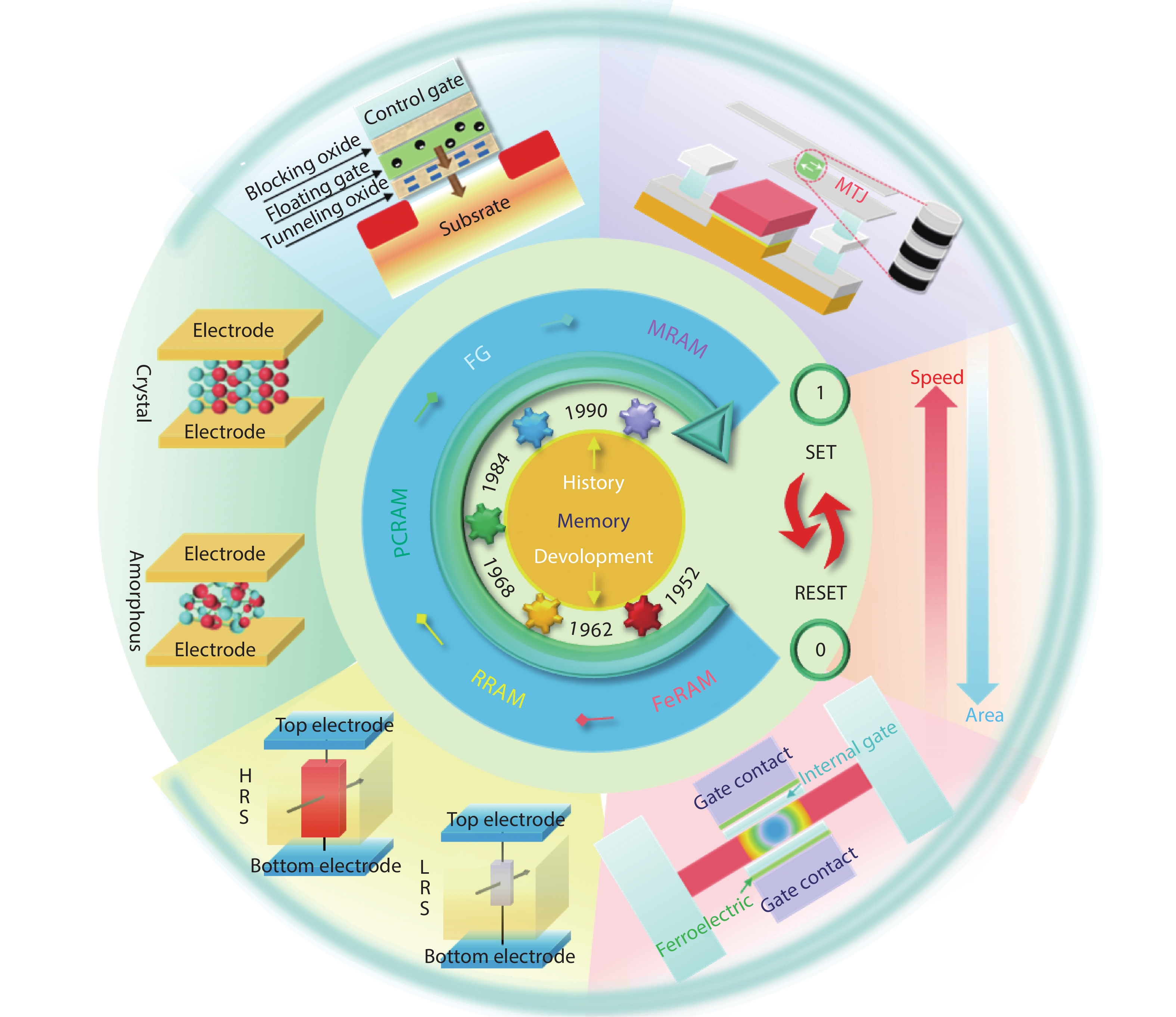
    Fig. 1. (Color online) Advanced non-volatile memory devices.
    (Color online) Overview of the in situ TEM characterization of memory devices in the wide range of external field stimuli, such as electrical, heating and magnetic fields.
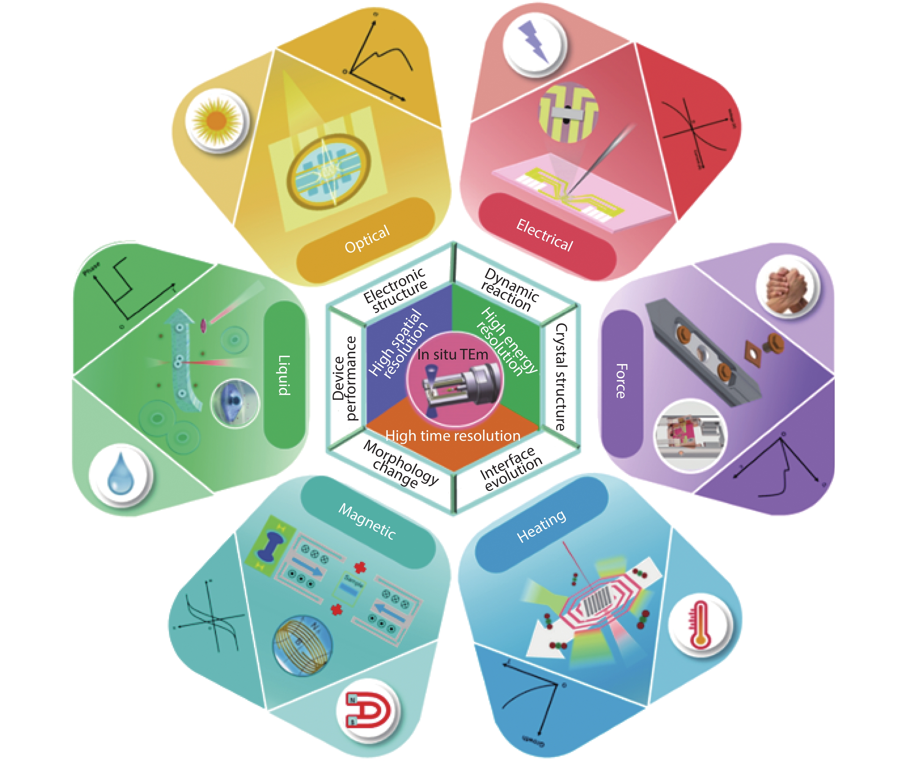
    Fig. 2. (Color online) Overview of the in situ TEM characterization of memory devices in the wide range of external field stimuli, such as electrical, heating and magnetic fields.
    (Color online) The switching mechanism of FeRAM and polarization evolution under the in situ environments. (a) Schematic of a typical FeRAM device. (b) Schematic diagram of polarization phenomenon in the SET/RESET process. (c) Structural changes of FeRAM during the switching of logic “0” and “1”. (d) HAADF-STEM image of polarization mapping in a BiFeO3/La0.7Sr0.3MnO3 based-FeRAM device. (e) Cross-sectional dark-field TEM images with different DWs. The scale bar is 20 nm. (f) Cross-sectional TEM images and corresponding diffraction patterns of the ferroelectric materials under the in situ electrical biasing field in the phase transition process. (g) A series of TEM dark-field images about the evolution of an upward polarized domain to a downward polarized matrix.
    Fig. 3. (Color online) The switching mechanism of FeRAM and polarization evolution under the in situ environments. (a) Schematic of a typical FeRAM device. (b) Schematic diagram of polarization phenomenon in the SET/RESET process. (c) Structural changes of FeRAM during the switching of logic “0” and “1”. (d) HAADF-STEM image of polarization mapping in a BiFeO3/La0.7Sr0.3MnO3 based-FeRAM device. (e) Cross-sectional dark-field TEM images with different DWs. The scale bar is 20 nm. (f) Cross-sectional TEM images and corresponding diffraction patterns of the ferroelectric materials under the in situ electrical biasing field in the phase transition process. (g) A series of TEM dark-field images about the evolution of an upward polarized domain to a downward polarized matrix.
    (Color online) The switching mechanism of RRAM and interfacial evolution under the in situ environments. (a) Schematic of the RRAM array. (b) Schematic diagrams of oxygen vacancies and MF-based resistive switching models in the SET/RESET process. (c) Local structural changes of the functional layer in RRAM during the switching of logic “0” and “1”. (d) The EELS oxygen K-edge spectra showing a lower oxygen count (more oxygen vacancies) in the device. (e) Topographic and electrostatic force microscopy results after removing the electrical stimuli suggesting that the charges observed should correspond to oxygen ions, instead of electrons. (f) A series of TEM images capturing the dynamic MF growth processes in the Cu/ZrO2/Pt TEM device. (g) Black-and-white images converted from the raw TEM images of (f) to highlight the growth of MF. (h) TEM images symbolizing logic “0” and “1” in the RS process. (i) A series of high-magnification TEM images showing the dynamic dissolution process of the MF.
    Fig. 4. (Color online) The switching mechanism of RRAM and interfacial evolution under the in situ environments. (a) Schematic of the RRAM array. (b) Schematic diagrams of oxygen vacancies and MF-based resistive switching models in the SET/RESET process. (c) Local structural changes of the functional layer in RRAM during the switching of logic “0” and “1”. (d) The EELS oxygen K-edge spectra showing a lower oxygen count (more oxygen vacancies) in the device. (e) Topographic and electrostatic force microscopy results after removing the electrical stimuli suggesting that the charges observed should correspond to oxygen ions, instead of electrons. (f) A series of TEM images capturing the dynamic MF growth processes in the Cu/ZrO2/Pt TEM device. (g) Black-and-white images converted from the raw TEM images of (f) to highlight the growth of MF. (h) TEM images symbolizing logic “0” and “1” in the RS process. (i) A series of high-magnification TEM images showing the dynamic dissolution process of the MF.
    (Color online) The switching mechanism of PCRAM and its nanostructure under the in situ environments. (a) Schematic of the PCRAM devices. (b) A schematic diagram of the phase change phenomenon occurs in the SET/RESET process. (c) The transformation between the crystal and amorphous phases in the memory devices from “0” to “1”. (d) A series of TEM images acquired during the in situ TEM heating field capturing the dynamic phase change process in the PCRAM device. The insets show the FFT patterns of the layer. (e) TEM images acquired showing the phase change under the in situ electrical biasing fields. (f, g) In situ amorphization of cubic GST at 300 °C with 200 keV e-beam irradiation, depicting the dynamic separation and shrinking of the cub-phase grains. The insets are the corresponding FFT patterns.
    Fig. 5. (Color online) The switching mechanism of PCRAM and its nanostructure under the in situ environments. (a) Schematic of the PCRAM devices. (b) A schematic diagram of the phase change phenomenon occurs in the SET/RESET process. (c) The transformation between the crystal and amorphous phases in the memory devices from “0” to “1”. (d) A series of TEM images acquired during the in situ TEM heating field capturing the dynamic phase change process in the PCRAM device. The insets show the FFT patterns of the layer. (e) TEM images acquired showing the phase change under the in situ electrical biasing fields. (f, g) In situ amorphization of cubic GST at 300 °C with 200 keV e-beam irradiation, depicting the dynamic separation and shrinking of the cub-phase grains. The insets are the corresponding FFT patterns.
    (Color online) The switching mechanism of floating-gate RAM and its nanostructure under the in situ environments. (a) Schematic of a typical floating-gate RAM device. (b) Schematic diagram of the charge storage in the memory device. (c) The corresponding internal oxygen vacancies distribution as the FG RAM transit from “0” to “1”. (d) Structural diagram of FG memory and high-resolution TEM images of the HfO2 capture layer. The white lines represent the position of grain boundaries. (e) A series of patterns concerning oxygen concentration in the trapping layer under the in situ electrical biasing fields. (f) Phase/potential mapping within the trapping layer at different biases. (g) Projected charge distribution at different biases in the trapping layer.
    Fig. 6. (Color online) The switching mechanism of floating-gate RAM and its nanostructure under the in situ environments. (a) Schematic of a typical floating-gate RAM device. (b) Schematic diagram of the charge storage in the memory device. (c) The corresponding internal oxygen vacancies distribution as the FG RAM transit from “0” to “1”. (d) Structural diagram of FG memory and high-resolution TEM images of the HfO2 capture layer. The white lines represent the position of grain boundaries. (e) A series of patterns concerning oxygen concentration in the trapping layer under the in situ electrical biasing fields. (f) Phase/potential mapping within the trapping layer at different biases. (g) Projected charge distribution at different biases in the trapping layer.
    (Color online) The switching mechanism of MRAM and its nanostructure by using advanced technology. (a) Schematic of the MRAM devices. (b) A schematic diagram of domain changes during the SET/RESET process. (c) Far-field diffraction pattern showing the different positions of the spectrometer entrance aperture for the left and right sidebands. Specific apertures are marked by yellow circles. (d) Schematic diagram of the EMCD technology working principle. (e) Raw achromatic SREELS image of the oxygen K edge and the Fe L3,2 edge of the double perovskite Sr2FeMoO6 without using an objective aperture. (f) Negative spherical aberration imaging of Sr2FeMoO6 and the corresponding projected structure model before tilting the sample. The arrows represent normalized background-subtracted SREELS images recorded at the O K edge. (g) Normalized background-subtracted SREELS image depicting the Fe L2,3 edge acquired at the ‘+’ and ‘−’ positions, respectively. (h) Atomic-scale image of EMCD achieved by subtracting the SREELS image acquired at the ‘+’ position from that acquired at the ‘−’ position.
    Fig. 7. (Color online) The switching mechanism of MRAM and its nanostructure by using advanced technology. (a) Schematic of the MRAM devices. (b) A schematic diagram of domain changes during the SET/RESET process. (c) Far-field diffraction pattern showing the different positions of the spectrometer entrance aperture for the left and right sidebands. Specific apertures are marked by yellow circles. (d) Schematic diagram of the EMCD technology working principle. (e) Raw achromatic SREELS image of the oxygen K edge and the Fe L3,2 edge of the double perovskite Sr2FeMoO6 without using an objective aperture. (f) Negative spherical aberration imaging of Sr2FeMoO6 and the corresponding projected structure model before tilting the sample. The arrows represent normalized background-subtracted SREELS images recorded at the O K edge. (g) Normalized background-subtracted SREELS image depicting the Fe L2,3 edge acquired at the ‘+’ and ‘−’ positions, respectively. (h) Atomic-scale image of EMCD achieved by subtracting the SREELS image acquired at the ‘+’ position from that acquired at the ‘−’ position.
    (Color online) The WB reliability of memory package. (a) Encapsulation diagram of the memory devices package. (b) A schematic diagram of the bonding void formation in the annealing process. (c) Cross-section focus ion beam image of the Cu-Al interface. (d–f) Lattice images and Fourier reconstructed pattern of CuAl2 (θ), CuAl (η2) and Cu9Al4 (γ2). (g) The STEM-BF image where the successive positions of the IMCs transformation interfaces, as indicated by the dashed lines. (h) Identification of sequential microstructure evolution of IMCs during the thermal annealing period under the in situ heating field.
    Fig. 8. (Color online) The WB reliability of memory package. (a) Encapsulation diagram of the memory devices package. (b) A schematic diagram of the bonding void formation in the annealing process. (c) Cross-section focus ion beam image of the Cu-Al interface. (d–f) Lattice images and Fourier reconstructed pattern of CuAl2 (θ), CuAl (η2) and Cu9Al4 (γ2). (g) The STEM-BF image where the successive positions of the IMCs transformation interfaces, as indicated by the dashed lines. (h) Identification of sequential microstructure evolution of IMCs during the thermal annealing period under the in situ heating field.
    Xin Yang, Chen Luo, Xiyue Tian, Fang Liang, Yin Xia, Xinqian Chen, Chaolun Wang, Steve Xin Liang, Xing Wu, Junhao Chu. A review of in situ transmission electron microscopy study on the switching mechanism and packaging reliability in non-volatile memory[J]. Journal of Semiconductors, 2021, 42(1): 013102
    Download Citation