Abstract
Non-volatile memory (NVM) devices with non-volatility and low power consumption properties are important in the data storage field. The switching mechanism and packaging reliability issues in NVMs are of great research interest. The switching process in NVM devices accompanied by the evolution of microstructure and composition is fast and subtle. Transmission electron microscopy (TEM) with high spatial resolution and versatile external fields is widely used in analyzing the evolution of morphology, structures and chemical compositions at atomic scale. The various external stimuli, such as thermal, electrical, mechanical, optical and magnetic fields, provide a platform to probe and engineer NVM devices inside TEM in real-time. Such advanced technologies make it possible for an in situ and interactive manipulation of NVM devices without sacrificing the resolution. This technology facilitates the exploration of the intrinsic structure-switching mechanism of NVMs and the reliability issues in the memory package. In this review, the evolution of the functional layers in NVM devices characterized by the advanced in situ TEM technology is introduced, with intermetallic compounds forming and degradation process investigated. The principles and challenges of TEM technology on NVM device study are also discussed.
1. Introduction
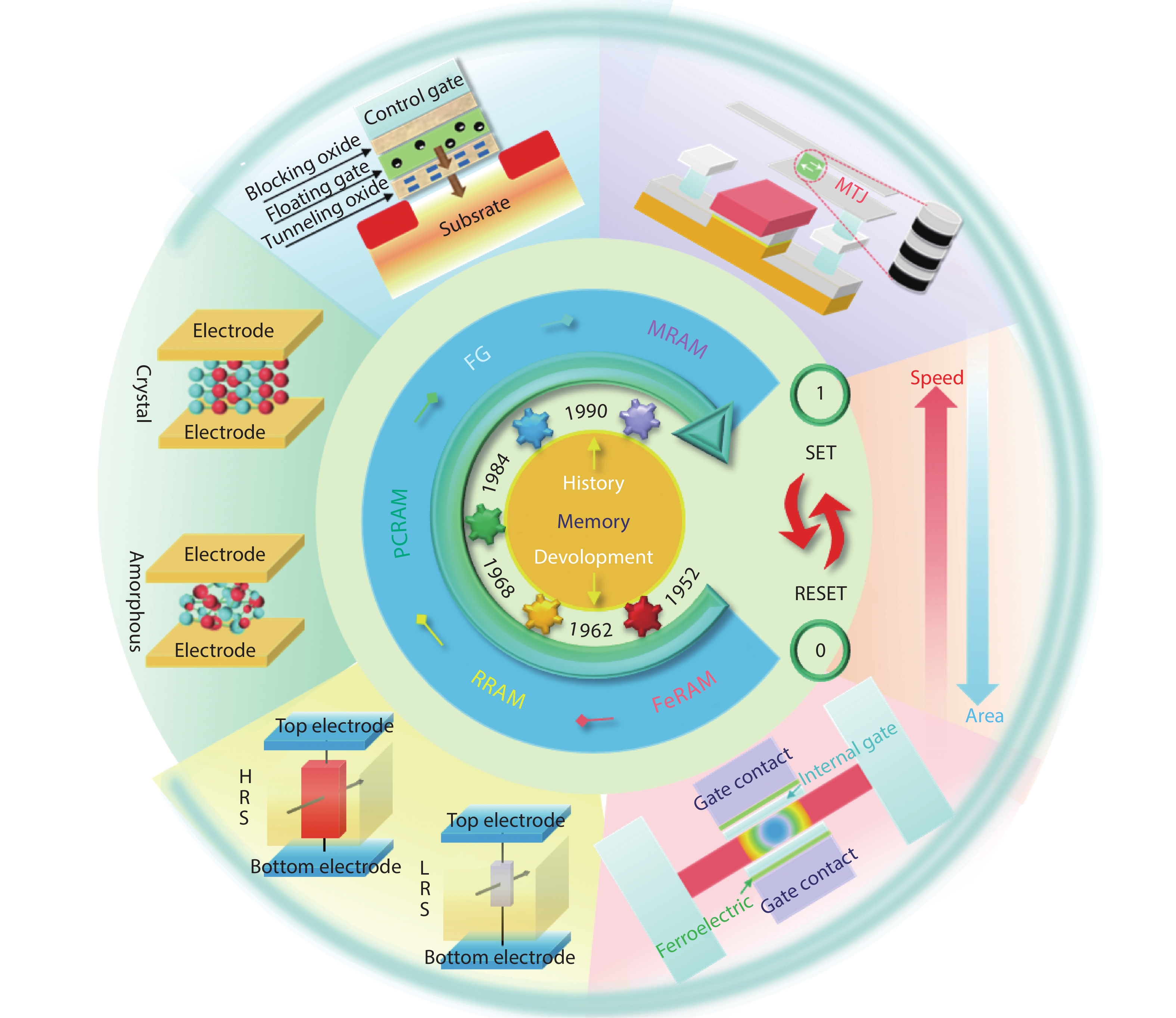
In the post-Moore era, non-volatile memories (NVMs) have rapidly evolved from the scientific study to digital products, including mobile devices, electronic instruments and artificial intelligence[1-8]. The properties of non-volatility and fast operation speed make NVMs the main data storage devices[9-13]. The NVMs with feasible miniaturization and scalability are important for high-density storage. The typical NVMs include ferroelectric random-access memory (FeRAM)[14-16], resistive random-access memory (RRAM)[17-20], phase-change random-access memory (PCRAM)[21-23], floating gate random-access memory (FG RAM)[24-27] and magnetic random-access memory (MRAM)[28-30]. The high capacity and density storage performances are governed by different switching mechanisms of NVMs. Fig. 1 shows the historic trends and structural schematics of the above typical NVMs in SET and RESET conditions. The NVMs are being developed towards higher speed and smaller volume[11-13].

Figure 1.(Color online) Advanced non-volatile memory devices.
The NVM package structure is important to chip performance as well[31-37]. NVMs tend to work under the electrical field and the heating field. These external energies have a great effect on the atomic structure of devices, which brings changes in device performance. Many experiments concerning in situ electrical and heating stimuli have been performed. Also, more external stimuli experiments needed to be explored for further studies on the device performance[38-42].
The evolution of microstructure and composition could be characterized using transmission electron microscopy (TEM) in real-time. TEM is undoubtedly a powerful tool to study the switching mechanism in miniaturized NVMs at atomic scale[1-3]. This advanced technology was firstly demonstrated by Max Knoll and Ernst Ruska in 1931. In 1939, the first commercial TEM was produced. Since then, tremendous effort has been made to improve the spatial and energy resolution. The TEM machines with field-emission guns could offer a spatial resolution close to 0.1 nm under the acceleration voltages between 200 and 300 kV. Currently, the most advanced TEM with aberration correctors could reach a spatial resolution of 0.5 Å[1, 2]. The energy resolution of TEM also reaches 0.01 eV which could image various elements clearly. In situ technology could provide various external fields to investigate the performance of the device by using different TEM sample holders. The time resolution of in situ TEM is in milliseconds. The combination of TEM and in situ technology provides a workable solution to visualize the intrinsic structure-switching mechanism of NVMs and intermetallic compounds (IMCs) reliability issues in packaging. Nowadays, various external stimuli, such as electrical, heating, force, light and magnetic sample holders are used to investigate mechanisms in NVMs under a high vacuum chamber environment without sacrificing the resolution[38-42]. As depicted in Fig. 2, with a variety of the in situ sample holders, the switching process could be dynamically monitored and manipulated under external stimuli simultaneously at the atomic scale[43-46]. The out circle represents different TEM holders that could perform in situ experiments. The sample holders ensure the external stimuli applied dynamically to realize various functions in the inner circle. In this review, we summarize the cutting-edge research on switching mechanisms of NVMs. The package reliability issue is also discussed. We primarily focus on in situ characterization techniques aiming to monitor and analyze the switching behavior of NVMs and IMCs at the atomic scale. Finally, a summary and outlook are provided for the bright future of the in situ TEM study in NVMs studies to improve device performance.
Figure 2.(Color online) Overview of the in situ TEM characterization of memory devices in the wide range of external field stimuli, such as electrical, heating and magnetic fields.
2. In situ study of non-volatile memories
2.1. Ferroelectric random-access memory
FeRAM is a promising non-volatile memory device for its low power consumption, fast work speed, and high reliability[16, 47-55]. The switching layer in FeRAM is the ferroelectric dielectric layer and the typical structure of FeRAM is depicted in Fig. 3(a). The ferroelectric materials have different polarization states under an external electrical field and Fig. 3(b) shows the corresponding structural diagram in the SET/RESET process. However, the switching mechanism is not clearly investigated by using traditional characterization tools. It is necessary to observe the microstructure changes directly. To understand the nature of switching states of FeRAM, a variety of in situ TEM experiments are performed[56-62].
Figure 3.(Color online) The switching mechanism of FeRAM and polarization evolution under the in situ environments. (a) Schematic of a typical FeRAM device. (b) Schematic diagram of polarization phenomenon in the SET/RESET process. (c) Structural changes of FeRAM during the switching of logic “0” and “1”. (d) HAADF-STEM image of polarization mapping in a BiFeO3/La0.7Sr0.3MnO3 based-FeRAM device. (e) Cross-sectional dark-field TEM images with different DWs. The scale bar is 20 nm. (f) Cross-sectional TEM images and corresponding diffraction patterns of the ferroelectric materials under the in situ electrical biasing field in the phase transition process. (g) A series of TEM dark-field images about the evolution of an upward polarized domain to a downward polarized matrix.
One of the methods to observe polarization states of FeRAM is the diffraction technique. The Bragg diffraction condition changes, owing to different crystal orientations and structure, and the contrast of images changes accordingly. For example, a typical BiFeO3 (BFO) film synthesized by standard solid-state reaction method consists of two phases: rhombohedral-like (R-like) phase and tetragonal-like (T-like) phase. The polarization of the two phases represents different resistance states with corresponding diffraction contrasts. Chiu et al. investigated the switching mechanism in BFO-based FeRAM and found that R-like and T-like structure transformed between each other during the SET/RESET process, as shown in Fig. 3(c)[56].
Generally speaking, the existence of defects and domain walls (DWs) could influence the device performance study. However, the microstructural changes of FeRAM during the switching process could not be observed directly by using the traditional characterization tools. In probing the effect of defects and DWs on the switching mechanism in FeRAM device working conditions, the application of electrical field in TEM is necessary. Currently, the spatial resolution of TEM has reached 0.5 Å and the accuracy of current measured could reach 10–12 A[1]. Benefitting from the high spatial and current resolution, Li et al. characterized the atomic replacement during the switching process on the BFO-based FeRAM device by using the in situ electrical TEM[61]. It was found that defects could bring the polarization back-switching, which results in the data loss shown in Fig. 3(d). Direct observation of the DWs evolution in the BFO is obtained by Pan et al. under the in situ electrical field[57]. During the switching process, the free charge accumulated near the DWs and strong charge DWs (sCDWs) formed. It was found that sCDWs could improve the steady metallic conductivity of FeRAM through angle changes in DWs, as shown in Fig. 3(e). The generation and disappearance of sCDWs affect the resistance changes for the device switching process. The dynamics of polarization in SET/RESET has been shown in Figs. 3(f) and 3(g)[56, 61].
Besides BFO, studies have been carried out on the ferroelectric KH2PO4 materials as well. The perovskite-type material-ABO3, such as BaTiO3, KNbO3, LiNbO3 and PZT (Pb(ZrTi)O3) become widely used[63]. Recent advances in atomic-level electron microscopy technology have made it possible to study high-quality FeRAM for its excellent work performance[64-67].
2.2. Resistive random-access memory
RRAM is a storage device that can switch between the low and high resistive states[19, 68-73]. A single memory unit is the metal–insulator–metal (MIM) structure with a dielectric layer sandwiched by a top electrode and a bottom electrode, as shown in Fig. 4(a). The switching behavior of the sandwich structure under a bias voltage was found by testing corresponding electrical characteristic curves. There are various explanations for the resistive phenomena in the MIM structure. Among these explanations, the widely accepted theoretical models are categorized into the interface resistance model and the filament conduction model. The interface resistance theory depends on the migration of oxygen atoms, and the filament conduction theory is based on the metal cations accumulation[73]. Fig. 4(b) depicts the schematic diagrams of the above two models. It is necessary to identify the structural changes in the two models[74-82]. To understand the nature of switching states of RRAM, a variety of in situ TEM experiments are performed for its high spatial and energy resolution for identifying the elements evolution during the switching process[83-87].
Figure 4.(Color online) The switching mechanism of RRAM and interfacial evolution under the in situ environments. (a) Schematic of the RRAM array. (b) Schematic diagrams of oxygen vacancies and MF-based resistive switching models in the SET/RESET process. (c) Local structural changes of the functional layer in RRAM during the switching of logic “0” and “1”. (d) The EELS oxygen K-edge spectra showing a lower oxygen count (more oxygen vacancies) in the device. (e) Topographic and electrostatic force microscopy results after removing the electrical stimuli suggesting that the charges observed should correspond to oxygen ions, instead of electrons. (f) A series of TEM images capturing the dynamic MF growth processes in the Cu/ZrO2/Pt TEM device. (g) Black-and-white images converted from the raw TEM images of (f) to highlight the growth of MF. (h) TEM images symbolizing logic “0” and “1” in the RS process. (i) A series of high-magnification TEM images showing the dynamic dissolution process of the MF.
The main RRAM mechanism could be divided into vacancies and filaments, which are the nature of interface resistance theory and the filament conduction theory. The vacancies and filaments both participate in the formation of conduction filaments in RRAM in some cases[74, 75]. The Z-contrast technology based on high-angle annular dark-field (HAADF)-STEM theory is capable of imaging the filament contrasts owing to the differences of the atomic number. For example, the Ni filament could be directly characterized using Z-contrast depicted in Fig. 4(c). Electron energy-loss spectroscopy (EELS) technique could identify the chemical elements. Electrons undergoing inelastic scattering could be collected by the energy loss spectrum. For example, fewer oxygen atoms could be observed in the oxide when a conductive channel forms in the device shown in Fig. 4(d)[76].
The understanding of the dynamics of oxygen vacancies in RRAM is important to improve device performance. As shown in Fig. 4(d), the relationship between oxygen vacancies and high conductivity channel has been studied[76]. It was found that oxygen vacancies accumulated under an applied electric field. Then these oxygen vacancies had a chemical reaction with metal cations accompanied by changes in the valence bond. Finally, a conductive channel formed. Also, electrostatic force microscopy could detect the existence of oxygen vacancies as shown in Fig. 4(e). Notably, the accumulated charge remained stable after biasing suggesting that the charge corresponds to oxygen ions rather than electrons[88].
The relationship between metal filaments (MFs) formation/rupture and resistive switching process is important to enhance device performance, and the nature of its working principle deserves investigation. Theoretically, the conductive filament occurs in a local region at the nanoscale[62]. When a positive voltage is applied to the active electrode, the mobile active metal ions drift to the anode surface. The MFs will form after the accumulation of metal ions during the switching process. In situ electric testing is the most feasible method for investigating the MFs. Liu et al. did the pioneering work to directly observe the formation and rupture of MFs as shown in Fig. 4(f)[77]. Fig. 4(g) is the black-and-white images converted from the raw TEM images of Fig. 4(f) to highlight the growth of MFs. Also, Ag particles could be discontinuously distributed to form a conductive channel. When the distance between multiple filaments meets the hopping distance of electrons in the electric field, the channel can be formed, as shown in Fig. 4(h). The microstructure and dynamic dissolution process of the MFs can be characterized using high-resolution TEM imaging, as shown in Fig. 4(i)[77].
Various materials can be used in RRAM. For example, typical materials used in the active electrode are Ag, Ti and Al. La0.67Sr0.33MnO3, SrTiO3, TiO2, ZrO2, Ag2S and Ta2O5 are commonly used materials for resistance material layer. Related research will be continuously promoted to improve the performance of RRAM[9] using in situ technology[89-96].
2.3. Phase change random-access memory
PCRAM with high integration and low power consumption is a promising NVM in the memory field. The construction of PCRAM is the MIM structure similar to the RRAM structure. The structure of PCRAM is shown in Fig. 5(a) and phase change in the dielectric layers are the core part[22, 97-103]. Phase change materials can transit between different phases with the corresponding resistance states displayed in Fig. 5(b). For example, Ge–Sb–Te (GST) exists in the two-phase change processes: from amorphous to face-centered cubic (FCC), and from FCC to hexagonal close packing (HCP). The GST exhibits semiconductor properties, semi-metallic properties, and metallic properties in the state of amorphous, FCC and HCP, respectively[104-106]. GST can transit from one phase to the other when applied to a critical voltage. A variety of in situ TEM experiments has been performed for the investigation on the nature of switching mechanisms in PCRAM[23, 107, 108].
Figure 5.(Color online) The switching mechanism of PCRAM and its nanostructure under the in situ environments. (a) Schematic of the PCRAM devices. (b) A schematic diagram of the phase change phenomenon occurs in the SET/RESET process. (c) The transformation between the crystal and amorphous phases in the memory devices from “0” to “1”. (d) A series of TEM images acquired during the in situ TEM heating field capturing the dynamic phase change process in the PCRAM device. The insets show the FFT patterns of the layer. (e) TEM images acquired showing the phase change under the in situ electrical biasing fields. (f, g) In situ amorphization of cubic GST at 300 °C with 200 keV e-beam irradiation, depicting the dynamic separation and shrinking of the cub-phase grains. The insets are the corresponding FFT patterns.
With the development of electron microscopy, the role of phase change play in the SET/RESET process deserves an in-depth study. Phase-contrast plays an important role in characterizing crystal structure during the switching process. The phase-contrast depends on the multiple diffraction beam coherent imaging through the aperture of the objective lens. The phase-contrast is sensitive to crystal structure and frequently used in the PCRAM studies as shown in Fig. 5(c).
The nanostructure changes during the switching process could be characterized directly by using in situ heating experiments. The heating sample holder is equipped with a micro-electro-mechanical system (MEMS) microheater by using a four-point probe that can measure the temperature changes. The temperature could reach a maximum of 1200 °C in a second without the sacrificing of atomic resolution. Fast Fourier transformation (FFT) is a method for the determination of phase structure. The interfacial spacing angle of the phase could be measured from FFT patterns to determine phase structure by comparing the data in the standard crystal library. For example, Lotnyk et al. performed in situ heating experiment on the GST sample. The FCC phase and HCP phase could be distinguished by the FFT method. It was found that the structure of the FCC phase is stable until the temperature increases up to 310 °C and transits to the stable GST HCP phase at the temperature of 320 °C shown in Fig. 5(d)[99].
Other in situ TEM technologies also play important roles in improving the performance of PCRAM, such as electrical field or e-beam radiation. Meister et al. used in situ electrical biasing fields to mimic the working environment[102]. It was found that the large crystalline phases disappeared during the electrical stressing as shown in Fig. 5(e). The structural changes brought resistance changes during the switching process. Also, the e-beam is a useful tool for the in situ manipulations of the crystal lattices to study the phase change. Jiang et al. studied the progressive amorphization of GST under the e-beam irradiation with different energies. The e-beam with higher energy leads to a more rapid amorphization process as shown in Figs. 5(f) and 5(g)[23].
Phase change materials used in PCRAM are developing. These materials could be categorized as: the binary alloy (GeTe), the ternary alloy (GeTeAs), and the multi-element alloy (AgInTeSb)[103-109]. These in situ images show that phase transition tends to occur through atomic displacement under external energy during the SET/RESET process. The dielectric layer phase changes could explain the above PCRAM instability by using the in situ TEM technology. To improve the performance of PCRAM, more advanced electron microscopy technologies and stable dielectric layer materials are needed[21, 110-117].
2.4. Floating gate random-access memory
Floating gate (FG) memory is important in the NVM market owing to the advantages of its high integration, high speed, low power consumption and good reliability. FG RAM is different from the previous memory devices. The charge could be stored in a floating gate layer[24-26, 118]. The schematic of the FG RAM devices is shown in Fig. 6(a), which has an extra capture layer compared to the traditional memory[118-124]. The extra capture layer between the gate and the substrate is to store the charge in the FG RAM. Based on the tunneling effect or hot electron injection effect, the charges pass through the capture layer for charging and discharging the floating gate. The specific charge movement process is shown in Fig. 6(b). However, the charge storage process could not be observed directly by using the traditional characterization tools. It is necessary to investigate the charge storage mechanism during the SET/RESET process. The electronic holography technique is used to directly observe charge storage.
Figure 6.(Color online) The switching mechanism of floating-gate RAM and its nanostructure under the in situ environments. (a) Schematic of a typical floating-gate RAM device. (b) Schematic diagram of the charge storage in the memory device. (c) The corresponding internal oxygen vacancies distribution as the FG RAM transit from “0” to “1”. (d) Structural diagram of FG memory and high-resolution TEM images of the HfO2 capture layer. The white lines represent the position of grain boundaries. (e) A series of patterns concerning oxygen concentration in the trapping layer under the in situ electrical biasing fields. (f) Phase/potential mapping within the trapping layer at different biases. (g) Projected charge distribution at different biases in the trapping layer.
Oxide materials with the high dielectric constant (κ) are widely used as the FG layer materials. The fabrication of the high κ layer is compatible with the semiconductor process. Li et al. investigated the oxygen vacancy-based conductive mechanism in the FG RAM in the HfO2 film[123]. Oxygen vacancies in HfO2 are induced when applied to a gate voltage as shown in Fig. 6(c).
The imaging technology based on the electric potential distribution is used to capture the distribution of oxygen vacancies. TEM equipped with electronic holography could visualize the electrical potential and morphology. The charge distribution could also be analyzed during the switching process. Fig. 6(d) displays the grain boundaries evolution due to the oxygen vacancies[125]. The accumulation of oxygen atoms could be observed in Fig. 6(e). The electric potential distribution is intuitively reflected by the e-beam phase distribution through the sample when the sample thickness is homogeneous. The electric potential distribution in the charge trapping layer under different gate bias is shown in Fig. 6(f).
How to link the charge distribution with the nanostructure of FGRAM is challenging. By taking advantage of the electrical potential and morphology, the charge distribution converted by the electric potential distribution could be obtained using the Poisson equation. This charge distribution has been further investigated[123]. As shown in Fig. 6(g), the charge distribution presents a non-uniform change with the increase of gate voltage values. The charge injected from some local places and reside there. This phenomenon could be explained by the non-uniform distribution of oxygen vacancies.
The traditional trapping layer materials are from SiO2 to the high κ materials. Combining the electronic holography technique, the charge movement of charge trapping memory is revealed. It confirms that the positive gate voltage induces oxygen vacancies. More advanced technologies are needed for further studies[126].
2.5. Magnetic random-access memory
MRAM is a typical memory device with long work lifetime, high work speed, low energy consumption and high capacity density compared with the conventional DRAM[30, 127-132]. Fig. 7(a) shows the schematic of the MRAM devices[133-140]. The data in MRAM is not stored as a charge or current flow, but by magnetic domain changes. As is shown in Fig. 7(b), the directions of domain changes when applied a voltage depicted by different colors[141]. However, the dynamic changes of the magnetic domain could not be observed by using conventional technology. Energy loss magnetic chiral dichroism (EMCD) technology has been contributed to study the MRAM switching mechanism[127-132].
Figure 7.(Color online) The switching mechanism of MRAM and its nanostructure by using advanced technology. (a) Schematic of the MRAM devices. (b) A schematic diagram of domain changes during the SET/RESET process. (c) Far-field diffraction pattern showing the different positions of the spectrometer entrance aperture for the left and right sidebands. Specific apertures are marked by yellow circles. (d) Schematic diagram of the EMCD technology working principle. (e) Raw achromatic SREELS image of the oxygen K edge and the Fe L3,2 edge of the double perovskite Sr2FeMoO6 without using an objective aperture. (f) Negative spherical aberration imaging of Sr2FeMoO6 and the corresponding projected structure model before tilting the sample. The arrows represent normalized background-subtracted SREELS images recorded at the O K edge. (g) Normalized background-subtracted SREELS image depicting the Fe L2,3 edge acquired at the ‘+’ and ‘−’ positions, respectively. (h) Atomic-scale image of EMCD achieved by subtracting the SREELS image acquired at the ‘+’ position from that acquired at the ‘−’ position.
The domain changes are subtle and transient and it is difficult for directly characterization magnetic structure of complex magnetic materials in microscopic regions[142]. The present occupant technology to characterize domain changes is X-ray magnetic chiral dichroism (XMCD)[143-145]. The signal of XMCD is produced by the virtual photons. The XMCD technique can distinguish the magnetic order of anti-ferromagnetism and ferromagnetism, which provides a new way to detect magnetic signals of materials. However, the spatial resolution is not high, owing to the wavelength of X-ray. Therefore, EMCD technology was developed and its signal is collected along with the EELS signal. The EELS are detected using electron beams from specific apertures marked by yellow circles as shown in Fig. 7(c). Compared to XMCD, it can distinguish the spin magnetic moment from the orbital magnetic moment at the nanometer scale, which means higher spatial resolution. Vortex beam with orbital angular momentum could be obtained under the e-beam modulation for the EMCD experiments. By analyzing the differences in the EMCD spectrum, information on the magnetic properties of the atom could be obtained.
The principle of the EMCD to observe domain changes is the second challenge needed to be discussed to better understand EMCD technology. The corresponding equipment details are shown in Fig. 7(d)[142-145]. It is possible to distinguish the magnetic properties of a given element by examining the EMCD spectrum at its characteristic energy.
The dynamics of imaging magnetic domain changes under the e-beam is important. Wang et al. studied the magnetic material – Sr2FeMoO6 (SMFO) exhibiting different types of magnetic coupling[128]. As shown in Fig. 7(e), the experimental achromatic spatially resolved EELS (SREELS) image of the double perovskite SFMO is depicted. Combining with the chromatic aberration correction with SREELS, their work demonstrated the atomic-scale imaging of EMCD from the individual Fe/Mo-O (004) atomic planes in the double perovskite SFMO. Fig. 7(f) reveals the arrangements of all atoms in the SFMO along with the [110]pc zone axis by the negative spherical aberration imaging technique. The pattern with arrows is the normalized background-subtracted SREELS images recorded at the oxygen K edge. The vertical spacing of 2 Å in the SREELS image at the oxygen K edge is consistent with the interplanar spacing between adjacent Fe/Mo-O and Sr-O atomic planes. The atomic-scale image of EMCD could be achieved by subtracting the SREELS images acquired at the ‘+’ and ‘–’ positions shown in Fig. 7(g). Fig. 7(h) shows the atomic-scale image of EMCD of SMFO from different SREELS images. The ratio of the spin to orbital magnetic moments could be obtained from the EMCD mapping to investigate the magnetism.
The EMCD technology is capable of understanding the physical origins of magnetic properties of materials at the highest spatial resolution. The principle of EMCD technology offers the possibility of achieving combined local atomic-scale magnetic, chemical and structural characterization. It is useful to promote technological development and improve device reliability in advanced MRAM technology[146-150].
3. In situ study of memory package
High integration density requires chip-level interconnection to ensure device performance. A high-quality memory package in NVMs is important for retaining the existing data under high working temperatures. The encapsulation diagram of the memory devices package is shown in Fig. 8(a). The pins of the circuit on the silicon chip are connected to the external joint with wires. This ultra-thin structure brings new challenges. The major one is the wire bonding (WB) lifetime under the high temperature. Intermetallic compound (IMC) formations between the two interfaces as-bonded conditions are critical for the WB lifetime, as shown in Fig. 8(b)[37]. It is difficult to find the failure area accurately at the nanoscale. However, combining TEM with various external field sample holders, it is possible to implement an in situ manipulation platform in TEM to observe the real-time evolution of materials[3].
Figure 8.(Color online) The WB reliability of memory package. (a) Encapsulation diagram of the memory devices package. (b) A schematic diagram of the bonding void formation in the annealing process. (c) Cross-section focus ion beam image of the Cu-Al interface. (d–f) Lattice images and Fourier reconstructed pattern of CuAl2 (θ), CuAl (η2) and Cu9Al4 (γ2). (g) The STEM-BF image where the successive positions of the IMCs transformation interfaces, as indicated by the dashed lines. (h) Identification of sequential microstructure evolution of IMCs during the thermal annealing period under the in situ heating field.
WB stability is important for NVM device performance. Among different WB materials, a copper alloy or palladium coated copper (PCC) is used to replace the conventional copper to prohibit oxidation. The chemical reactions of IMC under the thermal field changes the alloy stoichiometric. As shown in Fig. 8(c), take Cu–Al IMC as an example, the aluminum oxide as the protection layer is broken down and new IMCs formed. Various patents are proposed to improve performance such as the “integrated passive stacking for RFICs and MEMS in a system-in-package” by Liang et al.[151]. The patent provides a high level of circuit integration in a single molded package to improve device reliability.
The IMCs formed during the annealing process consists of multiple metal compounds. The delamination or void growth occurs when the IMCs are under the thermal field[31]. Kim et al. studied the compositions of Cu–Al IMCs under annealing process by using the TEM technique[150]. It is founded that CuAl2 (θ), CuAl (η2) and Cu9Al4 (γ2) are the main structures in the IMCs during the annealing process. The different structures of IMCs could be measured by using FFT patterns as shown in Figs. 8(d)–8(f). The delamination or void growth occurs are uneven on the Cu–Al surface shown in Fig. 8(g).
By studying the mechanism of WB microstructure evolution under the heating field, the nature of IMCs could be observed dynamically[34, 152-154]. The IMC mechanism was further studied by Xu et al.[36]. The process of IMCs growth and phase transition were in situ recorded in Fig. 8(h). The annealing process occurred in the chamber of TEM using a thermal sample holder, and the evolution of the bonding interfacial structure could be dynamically observed. A bilayer of IMCs with CuAl2 and Cu9Al4 formed. The CuAl2 started transforming into CuAl when the Al pad was consumed greatly. With the continuous decrease of Al element, the CuAl layer and CuAl2 transformed into Cu9Al4 under the annealing process as shown in Fig. 8(h). The final phase in IMC is the Cu9Al4.
Memory package is an important field in the semiconductor industry and its reliability greatly affects the device performance. More advanced electron microscopy will be used to study the package stability issues.
4. Conclusion
The NVMs characterized by the in situ TEM techniques combined with multiple stimuli such as e-beam, electrical field, heating field have been reviewed in this article. The switching mechanisms during the SET/RESET process have been discussed as well. From the above experiments and discussions, the future development directions, performance optimizations, characterization tools improvement and reliability research are all pointed out.
In the future, more advanced in situ experiments are needed, such as force or optical fields combined with TEM. As the continued scaling down memory devices, the high efficiency and the versatility of in situ TEM techniques are needed. The physical mechanism of the memory devices, such as the charge storage, DWs inverse, negative capacitance effect and so on[155-158]. The next generation TEM techniques should aim to provide a comprehensive analysis with higher spatial resolution and energy resolution[4, 159].
Here, we summarized the current applications and technical challenges for employing in situ TEM techniques on the mechanism study of NVMs as the following three aspects:
(1) The resolution of light element for TEM image should be improved[160-163]. For example, the in situ study in FeRAM requires the observation of oxygen atom displacement at a subtle scale. There is plenty of room to improve the spatial resolution combining various contrast principles such as increasing the acceleration voltage, adding an objective lens and the dyeing corresponding compositions.
(2) Advanced technical developments are needed about in situ TEM to observe the charge storage in the memory devices. The electronic holography method is an effective tool for imaging the electron potential distribution. A faster charge-coupled device (CCD) and big data technology are needed to record the process. The current time resolution of TEM equipped with CCD can reach a picosecond level[164, 165]. Faster CCD could improve TEM time resolution during the characterization of the switching process[166-168].
(3) EMCD is a powerful technique for the in situ studies of MRAM. The dynamic observation of magnetic domains could be implemented under a high time resolution[169-173].
The development of information technology has greatly promoted the memory storage density and speed[174-180]. Electron microscopy, especially the in situ TEM technology provides an opportunity to study the dynamic structural evolution to better understand the physical mechanism of the memory device.
Acknowledgements
This work is supported by the Projects of Science and Technology Commission of Shanghai Municipality (19ZR1473800 and 14DZ2260800), the Shanghai Rising-Star Program (17QA1401400), Young Elite Scientists Sponsorship Program by CAST (YESS), and the Fundamental Research Funds for the Central Universities.
References
[1] et alIn situ transmission electron microscopy characterization and manipulation of two-dimensional layered materials beyond graphene. Small, 13, 1604259(2017).
[2] et alElectron ptychography of 2D materials to deep sub-ångström resolution. Nature, 559, 343(2018).
[3] et alDynamic structure-properties characterization and manipulation in advanced nanodevices. Mater Today Nano, 7, 100042(2019).
[4] et alRecommended methods to study resistive switching devices. Adv Electron Mater, 5, 1800143(2019).
[5] et alIn situ transmission electron microscopy for energy materials and devices. Adv Mater, 31, 1900608(2019).
[6] et alDirect covalent modification of black phosphorus quantum dots with conjugated polymers for information storage. Nanoscale, 11, 3527(2019).
[7] et alAn overview of nonvolatile emerging memories: Spintronics for working memories. IEEE J Emerg Sel Top Circuits Syst, 6, 109(2016).
[8] et alMemory materials and devices: From concept to application. InfoMat, 2, 261(2020).
[9] et alUnderstanding memristive switching via in situ characterization and device modeling. Nat Commun, 10, 3453(2019).
[10] Nanoscale resistive switching devices for memory and computing applications. Nano Res, 13, 1228(2020).
[11] et alBrain-inspired computing with memristors: Challenges in devices, circuits, and systems. Appl Phys Rev, 7, 011308(2020).
[12] et alFunctional non-volatile memory devices: From fundamentals to photo-tunable properties. Phys Status Solidi RRL, 13, 1970022(2019).
[13] Microscopic investigations of switching phenomenon in memristive systems: A mini review. RSC Adv, 8, 28763(2018).
[14] et alTransparent, flexible, fatigue-free, optical-read, and nonvolatile ferroelectric memories. ACS Appl Mater Interfaces, 11, 35169(2019).
[15] et alA ferroelectric semiconductor field-effect transistor. Nat Electron, 2, 580(2019).
[16] et alImprovement of endurance in HZO-based ferroelectric capacitor using Ru electrode. IEEE Electron Device Lett, 40, 1744(2019).
[17] et alResistance random access memory. Mater Today, 19, 254(2016).
[18] Overview of resistive random access memory (RRAM): Materials, filament mechanisms, performance optimization, and prospects. Phys Status Solidi RRL, 13, 1900073(2019).
[19] et alAll nonmetal resistive random access memory. Sci Rep, 9, 6144(2019).
[20] et alA review of recent applications of ion beam techniques on nanomaterial surface modification: Design of nanostructures and energy harvesting. Small, 15, 1901820(2019).
[21] et alDesigning crystallization in phase-change materials for universal memory and neuro-inspired computing. Nat Rev Mater, 4, 150(2019).
[22] et alRecent progress in phase-change_newline memory technology. IEEE J Emerg Sel Top Circuits Syst, 6, 146(2016).
[23] et alProgressive amorphization of GeSbTe phase-change material under electron beam irradiation. APL Mater, 7, 081121(2019).
[24] et alA semi-floating gate transistor for low-voltage ultrafast memory and sensing operation. Science, 341, 640(2013).
[25] et alInvestigation of device physics and modeling of semi-floating gate image sensor cell. Microelectron Eng, 217, 111111(2019).
[26] et alSelf-assembled Sn nanocrystals as the floating gate of nonvolatile flash memory. ACS Appl Electron Mater, 1, 1852(2019).
[27] et alIn situ electron holography study of charge distribution in high-κ charge-trapping memory. Nat Commun, 4, 2764(2013).
[28] et alThree-dimensional nanomagnetism. Nat Commun, 8, 15756(2017).
[29] et alFully epitaxial magnetic tunnel junction on a silicon wafer. Appl Phys Lett, 115, 202403(2019).
[30] et alMagnetic skyrmions in FePt nanoparticles having Reuleaux 3D geometry: A micromagnetic simulation study. Nanoscale, 11, 20102(2019).
[31] et alInterface evolution of Cu–Ni–Si/Al–Mg–Si clad composite wires after annealing. Rare Met, 42, 1(2018).
[32] Investigation of the early stage of reactive interdiffusion in the Cu-Al system by in situ transmission electron microscopy. Materialia, 9, 100633(2020).
[33] et alBehavior of aluminum oxide, intermetallics and voids in Cu–Al wire bonds. Acta Mater, 59, 5661(2011).
[34] et alCu–Al interfacial formation and kinetic growth behavior during HTS reliability test. J Mater Process Technol, 267, 90(2019).
[35]
[36] et alNew observation of nanoscale interfacial evolution in micro Cu–Al wire bonds by in situ high resolution TEM study. Scr Mater, 115, 1(2016).
[37] et alCu–Al intermetallic compound investigation using ex-situ post annealing and in situ annealing. Microelectron Reliab, 55, 2316(2015).
[38] In situ transmission electron microscopy and spectroscopy studies of rechargeable batteries under dynamic operating conditions: A retrospective and perspective view. J Mater Res, 30, 326(2015).
[39] In situ mechanical TEM: Seeing and measuring under stress with electrons. Comptes Rendus Physique, 15, 224(2014).
[40] et alIn situ TEM near-field optical probing of nanoscale silicon crystallization. Nano Lett, 12, 2524(2012).
[41] et alControlled growth of nanoparticles from solution with in situ liquid transmission electron microscopy. Nano Lett, 11, 2809(2011).
[42] et alIn situ magnetic study of the low-temperature oxidation of carbon-supported cobalt nanoparticles. J Phys Chem C, 111, 5576(2007).
[43] Electron tomography and holography in materials science. Nat Mater, 8, 271(2009).
[44] Imaging of magnetic and electric fields by electron microscopy. J Phys: Condens Matter, 28, 403001(2016).
[45]
[46] et alIn situ observation of voltage-induced multilevel resistive switching in solid electrolyte memory. Adv Mater, 23, 3272(2011).
[47] et alA direct observation on the structure evolution of memory-switching phenomena using in situ TEM. 2009 Symposium on VLSI Technology, 204(2009).
[48] et alResistive switching studies of ReRAM devices by in situ TEM. Microsc Microanal, 25, 71(2019).
[49] et alCharacterization of atomic defects on the photoluminescence in two-dimensional materials using transmission electron microscope. InfoMat, 1, 85(2019).
[50] et alElectrode material dependent breakdown and recovery in advanced high-κ gate stacks. Appl Phys Lett, 96, 202903(2010).
[51] et alRecent advances in two-dimensional ferromagnetism: Materials synthesis, physical properties and device applications. Nanoscale, 12, 2309(2020).
[52] Self-assembled multiferroic perovskite–spinel nanocomposite thin films: Epitaxial growth, templating and integration on silicon. J Mater Chem C, 7, 9128(2019).
[53] et alThe electrical enhancement and reversible manipulation of near-infrared luminescence in Nd doped ferroelectric nanocomposites for optical switches. J Mater Chem C, 7, 4320(2019).
[54] et alEffect of extrinsically introduced passive interface layer on the performance of ferroelectric tunnel junctions. ACS Appl Mater Interfaces, 9, 5050(2017).
[55] Physics and applications of bismuth ferrite. Adv Mater, 21, 2463(2009).
[56] et alIn-situ TEM observation of multilevel storage behavior in low power FeRAM device. Nano Energy, 34, 103(2017).
[57] et alGiant resistive switching via control of ferroelectric charged domain walls. Adv Mater, 28, 6574(2016).
[58] et alQuantitative experimental determination of site-specific magnetic structures by transmitted electrons. Nat Commun, 4, 1395(2013).
[59] et alAtomic resolution probing of phase transformations and domain evolution during large superelastic deformation in ferroelectrics with in situ TEM. Microsc Microanal, 25, 1850(2019).
[60] Multiferroic and magnetoelectric materials. Nature, 442, 759(2006).
[61] et alAtomic-scale mechanisms of defect-induced retention failure in ferroelectrics. Nano Lett, 17, 3556(2017).
[62] et alAtomic scale modulation of self-rectifying resistive switching by interfacial defects. Adv Sci, 5, 1800096(2018).
[63] The physics of ferroelectric memories. Phys Today, 51, 22(1998).
[64] et alDeterministic ferroelastic domain switching using ferroelectric bilayers. Nano Lett, 19, 5319(2019).
[65]
[66] et alConfigurable resistive response in BaTiO3 ferroelectric memristors via electron beam radiation. Adv Mater, 32, 1907541(2020).
[67] et alInfluence of high-pressure annealing on memory properties of Hf0.5Zr0.5O2 based 1T-FeRAM. IEEE Electron Device Lett, 40, 1076(2019).
[68] et alHighly flexible and stable resistive switching devices based on WS2 nanosheets: Poly(methylmethacrylate) nanocomposites. Sci Rep, 9, 19316(2019).
[69] et alA novel resistive switching identification method through relaxation characteristics for sneak-path-constrained selectorless RRAM application. Sci Rep, 9, 12420(2019).
[70] et al3D characterization of hard breakdown in RRAM device. Microelectron Eng, 216, 111042(2019).
[71] et alResistive switching mechanism in the one diode-one resistor memory based on p+-Si/n-ZnO heterostructure revealed by in situ TEM. Sci Rep, 7, 45143(2017).
[72] et alControlling resistive switching by using an optimized MoS2 interfacial layer and the role of top electrodes on ascorbic acid sensing in TaOx-based RRAM. Langmuir, 35, 3897(2019).
[73] et alHighly durable and flexible gallium-based oxide conductive-bridging random access memory. Sci Rep, 9, 14141(2019).
[74] et alSub-10 nm Ta channel responsible for superior performance of a HfO2 memristor. Sci Rep, 6, 28525(2016).
[75] et alMemory devices: Direct observations of nanofilament evolution in switching processes in HfO2-based resistive random access memory by in situ TEM studies. Adv Mater, 29, 1602976(2017).
[76] The nature of dielectric breakdown. Appl Phys Lett, 93, 072903(2008).
[77] et alReal-time observation on dynamic growth/dissolution of conductive filaments in oxide-electrolyte-based ReRAM. Adv Mater, 24, 1844(2012).
[78] et alCorrelation of structural modifications by multiscale phase mapping in filamentary type HfO2-based RRAM: Towards a component specific in situ TEM investigation. Microsc Microanal, 25, 1842(2019).
[79] et alGermanium as a sodium ion battery material: In situ TEM reveals fast sodiation kinetics with high capacity. Chem Mater, 28, 1236(2016).
[80] et alEnhanced stability of filament-type resistive switching by interface engineering. Sci Rep, 7, 43664(2017).
[81] et alEvolution of filament formation in Ni/HfO2/SiOx/Si-based RRAM devices. Adv Electron Mater, 1, 1500130(2015).
[82]
[83] et alElectrochemical dynamics of nanoscale metallic inclusions in dielectrics. Nat Commun, 5, 4232(2014).
[84] et alFilament growth dynamics in solid electrolyte-based resistive memories revealed by in situ TEM. Nano Res, 7, 1065(2014).
[85] et alDynamic evolution of conducting nanofilament in resistive switching memories. Nano Lett, 13, 3671(2013).
[86] et alElectric-field induced structural transition in vertical MoTe2- and Mo1–xWxTe2-based resistive memories. Nat Mater, 18, 55(2019).
[87] et alCharge transition of oxygen vacancies during resistive switching in oxide-based RRAM. ACS Appl Mater Interfaces, 11, 11579(2019).
[88] et alProbing nanoscale oxygen ion motion in memristive systems. Nat Commun, 8, 15173(2017).
[89] et alAll WSe2 1T1R resistive RAM cell for future monolithic 3D embedded memory integration. Nat Commun, 10, 5201(2019).
[90] et alMulti-factors induced evolution of resistive switching properties for TiN/Gd2O3/Au RRAM devices. J Alloy Compd, 816, 152564(2020).
[91] et alTernary content-addressable memory with MoS2 transistors for massively parallel data search. Nat Electron, 2, 108(2019).
[92] et alAn indirect way to achieve comprehensive performance improvement of resistive memory: When hafnium meets ITO in an electrode. Nanoscale, 12, 3267(2020).
[93] Metal-oxide resistive random access memory (RRAM) technology: Material and operation details and ramifications. In: Advances in Non-Volatile Memory and Storage Technology. Amsterdam: Elsevier, 35(2019).
[94] Nano resistive memory (Re-RAM) devices and their applications. Rev Adv Mater Sci, 58, 248(2019).
[95] et alReview of printed electrodes for flexible devices. Front Mater, 5, 77(2019).
[96] et alA general and facile method for preparation of large-scale reduced graphene oxide films with controlled structures. Carbon, 143, 162(2019).
[97] et alSwitching between crystallization from the glassy and the undercooled liquid phase in phase change material Ge2Sb2Te5. Adv Mater, 31, 1900784(2019).
[98] et alKinetics features conducive to cache-type nonvolatile phase-change memory. Chem Mater, 31, 8794(2019).
[99] Phase change thin films for non-volatile memory applications. Nanoscale Adv, 1, 3836(2019).
[100] et alPhase change materials and phase change memory. MRS Bull, 39, 703(2014).
[101] et alSc-centered octahedron enables high-speed phase change memory with improved data retention and reduced power consumption. ACS Appl Mater Interfaces, 11, 10848(2019).
[102] et alIn situ transmission electron microscopy observation of nanostructural changes in phase-change memory. ACS Nano, 5, 2742(2011).
[103]
[104] An extremely fast, energy-efficient RESET process in Ge2Sb2Te5 phase change memory device revealed by the choice of electrode materials and interface effects. Semicond Sci Technol, 35, 015022(2020).
[105] et alBipolar resistive switching of Ge2Sb2Te5 material. Proc SPIE 11209, Eleventh International Conference on Information Optics and Photonics (CIOP 2019), 1120, 1120939(2019).
[106] et alBipolar resistive switching behavior of an amorphous Ge2Sb2Te5 thin films with a Te layer. Nanoscale, 7, 6340(2015).
[107] et alDirect measurement of crystal growth velocity in epitaxial phase-change material thin films. ACS Appl Mater Interfaces, 11, 41544(2019).
[108] et alIn situ TEM study of electron-beam radiation induced boron diffusion and effects on phase and microstructure evolution in nanostructured CoFeB/SiO2 thin film. J Appl Phys, 121, 015111(2017).
[109] et alIn-situ characterization of switching mechanisms in phase change random access memory (PRAM) using transmission electron microscopy (TEM). IEEE International Symposium for Testing and Failure Analysis, 236(2013).
[110] et alIn-situ TEM analysis of the phase transformation mechanism of a Cu–Al–Ni shape memory alloy. J Alloy Compd, 808, 151743(2019).
[111] et alIn situ observation of crystalline silicon growth from SiO2 at atomic scale. Research, 2019, 1(2019).
[112] et alIn-situ observation of Ge2Sb2Te5 crystallization at the passivated interface. Ceram Int, 45, 19542(2019).
[113] et alDirect atomic insight into the role of dopants in phase-change materials. Nat Commun, 10, 3525(2019).
[114] et alPhase-change memories (PCM) – Experiments and modelling: General discussion. Faraday Discuss, 213, 393(2019).
[115] Catching structural transitions in liquids. Science, 364, 1032(2019).
[116]
[117] et alGeSbTe deposition for the PRAM application. Appl Surf Sci, 253, 3969(2007).
[118] et alWafer-scale transferred multilayer MoS2 for high performance field effect transistors. Nanotechnology, 30, 174002(2019).
[119] et alThe relationship between the dislocations and microstructure in In0.82Ga0.18As/InP heterostructures. Sci Rep, 6, 35139(2016).
[120] et alTwo-terminal floating-gate memory with van der Waals heterostructures for ultrahigh on/off ratio. Nat Commun, 7, 12725(2016).
[121] et alHigh-performance nonvolatile organic transistor memory using quantum dots-based floating gate. IEEE Trans Electron Devices, 64, 3816(2017).
[122] et alTransparent and flexible graphene charge-trap memory. ACS Nano, 6, 7879(2012).
[123] et alIn situ transmission electron microscopy studies on nanomaterials and HfO2-based storage nanodevices. Acta Phys Sin, 67, 124(2018).
[124] et alQuantitative mapping of the charge density in a monolayer of MoS2 at atomic resolution by off-axis electron holography. ACS Nano, 14, 524(2020).
[125] Quantitative measurement of nanoscale electrostatic potentials and charges using off-axis electron holography: Developments and opportunities. Ultramicroscopy, 203, 105(2019).
[126]
[127] Production and application of electron vortex beams. Nature, 467, 301(2010).
[128] et alAtomic scale imaging of magnetic circular dichroism by achromatic electron microscopy. Nat Mater, 17, 221(2018).
[129] et alEffects of dynamic diffraction conditions on magnetic parameter determination in a double perovskite Sr2FeMoO6 using electron energy-loss magnetic chiral dichroism. Ultramicroscopy, 176, 212(2017).
[130] et alQuantitative characterization of nanoscale polycrystalline magnets with electron magnetic circular dichroism. Nat Commun, 5, 3138(2014).
[131] et alElement-specific magnetic hysteresis of individual 18 nm Fe nanocubes. Nano Lett, 11, 1710(2011).
[132] et alMagnetic monopole field exposed by electrons. Nat Phys, 10, 26(2014).
[133] et alUltrathin perpendicular magnetic anisotropy CoFeB free layers for highly efficient, high speed writing in spin-transfer-torque magnetic random access memory. Sci Rep, 9, 19407(2019).
[134] Magnetic properties and oxygen migration induced resistive switching effect in Y substituted multiferroic bismuth ferrite. Phys Chem Chem Phys, 21, 15854(2019).
[135] et alMagnetic measurements with atomic-plane resolution. Nat Commun, 7, 12672(2016).
[136] et alEvaluation of a new MgO barrier based on CoFeB/MgO/CoFeB structure for advanced MRAM applications. Microelectron Eng, 167, 6(2017).
[137] et alEvidence of intrinsic ferromagnetism in individual dilute magnetic semiconducting nanostructures. Nat Nanotech, 4, 523(2009).
[138] et alInnovative approaches to the invisible defect on STT-MRAM. Microelectron Reliab, 100/101, 113431(2019).
[139] et alColossal magnetoresistance in La–Ca–Mn–O ferromagnetic thin films. J Appl Phys, 76, 6929(1994).
[140] et alEnergy-efficient ultrafast SOT-MRAMs based on low-resistivity spin hall metal Au0.25Pt0.75. Adv Electron Mater, 6, 1901131(2000).
[141] et alNon-destructive imaging for quality assurance of magnetoresistive random-access memory junctions. J Phys D, 53, 014004(2019).
[142] First-principles theory of chiral dichroism in electron microscopy applied to 3d ferromagnets. Phys Rev B, 75, 214425(2007).
[143] et alQuantitative EMCD by use of a double aperture for simultaneous acquisition of EELS. Ultramicroscopy, 196, 192(2019).
[144] et alBlind identification of magnetic signals in electron magnetic chiral dichroism using independent component analysis. Ultramicroscopy, 195, 129(2018).
[145] et alTowards quantitative nanomagnetism in transmission electron microscope by the use of patterned apertures. Microsc Microanal, 25, 654(2019).
[146] et alMapping inelastic intensities in diffraction patterns of magnetic samples using the energy spectrum imaging technique. Ultramicroscopy, 108, 393(2008).
[147] et alDomain wall spin structures in mesoscopic Fe rings probed by high resolution SEMPA. J Phys D, 49, 425004(2016).
[148] et alRecent progress and next directions for embedded MRAM technology. 2019 Symposium on VLSI Circuits, T190(2019).
[149] et alMagnetoresistive random access memory: Present and future. IEEE Trans Electron Devices, 67, 1407(2020).
[150] et alEffects of Cu/Al intermetallic compound (IMC) on copper wire and aluminum pad bondability. IEEE Trans Comp Packag Technol, 26, 367(2003).
[151]
[152]
[153] et alMicrostructural indicators for prognostication of copper–aluminum wire bond reliability under high-temperature storage and temperature humidity. IEEE Trans Compon Packag Manuf Technol, 6, 569(2016).
[154] et alIntermetallic compound growth and stress development in Al–Cu diffusion couple. J Electron Materi, 47, 855(2018).
[155] et alMetallic few-layered VSe2 nanosheets: High two-dimensional conductivity for flexible in-plane solid-state supercapacitors. J Mater Chem A, 6, 8299(2018).
[156] et alVSe2/carbon-nanotube compound for all solid-state flexible in-plane supercapacitor. Appl Phys Lett, 114, 023902(2019).
[157] et alPalladium diselenide long-wavelength infrared photodetector with high sensitivity and stability. ACS Nano, 13, 2511(2019).
[158] et alSubstrates and interlayer coupling effects on Mo1–xWxSe2 alloys. J Semicond, 40, 062005(2019).
[159] et alIn situ transmission electron microscopy for energy applications. Joule, 3, 4(2019).
[160]
[161] et alHigh efficiency and fast van der Waals hetero-photodiodes with a unilateral depletion region. Nat Commun, 10, 4663(2019).
[162] et alIn situ interfacial manipulation of metastable states between nucleation and decomposition of single bismuth nanoparticle. Phys Status Solidi B, 256, 1970016(2019).
[163] et alInterfacial defects: Probing and manipulating the interfacial defects of InGaAs dual-layer metal oxides at the atomic scale. Adv Mater, 30, 1870013(2018).
[164] et al4D imaging of transient structures and morphologies in ultrafast electron microscopy. Science, 322, 1227(2008).
[165] et alImaging rotational dynamics of nanoparticles in liquid by 4D electron microscopy. Science, 355, 494(2017).
[166] et alElectronic holographic three-dimensional display with enlarged viewing angle using non-mechanical scanning technology. OSA Continuum, 2, 1917(2019).
[167] et alIn-situ studies of magnetostriction in TbxHo1–xFe1.9Mn0.1 Laves compounds. J Magn Magn Mater, 501, 166422(2020).
[168] Electron holography: Phase imaging with nanometer resolution. Ann Rev Mater Res, 37, 729(2007).
[169] et alReciprocal and real space maps for EMCD experiments. Ultramicroscopy, 110, 1380(2010).
[170] Atomic-plane resolved electron magnetic circular dichroism by achromatic spatially-resolved electron energy loss spectroscopy. Microsc Microanal, 25, 572(2019).
[171] et alElectron vortex beams prepared by a spiral aperture with the goal to measure EMCD on ferromagnetic films via STEM. Ultramicroscopy, 150, 16(2015).
[172] et alDetection of magnetic circular dichroism using a transmission electron microscope. Nature, 441, 486(2006).
[173] et alProspect for detecting magnetism of a single impurity atom using electron magnetic chiral dichroism. Phys Rev B, 100, 104434(2019).
[174] et alStructure-property relationships in graphene-based strain and pressure sensors for potential artificial intelligence applications. Sensors, 19, 1250(2019).
[175] et alDual-mode sensor and actuator to learn human-hand tracking and grasping. IEEE Trans Electron Devices, 66, 5407(2019).
[176] et alUltrafast dynamic pressure sensors based on graphene hybrid structure. ACS Appl Mater Interfaces, 9, 24148(2017).
[177] et alProperties of graphene-metal contacts probed by Raman spectroscopy. Carbon, 127, 491(2018).
[178] et alIn situ dynamic manipulation of graphene strain sensor with drastically sensing performance enhancement. Adv Electron Mater, 6, 2000269(2020).
[179] et alIron-doped VSe2 nanosheets for enhanced hydrogen evolution reaction. Appl Phys Lett, 116, 223901(2020).
[180] et alIn situ interfacial sublimation of Zn2GeO4 nanowire for atomic-scale manufacturing. ACS Appl Nano Mater, 3, 4747(2020).