
Jing-Zhi Huang, Zi-Tao Ji, Jia-Jian Chen, Wen-Qi Wei, Jia-Le Qin, Zi-Hao Wang, Zhi-Yuan Li, Ting Wang, Xi Xiao, Jian-Jun Zhang, "Ultra-broadband flat-top quantum dot comb lasers," Photonics Res. 10, 1308 (2022)
- Photonics Research
- Vol. 10, Issue 5, 1308 (2022)
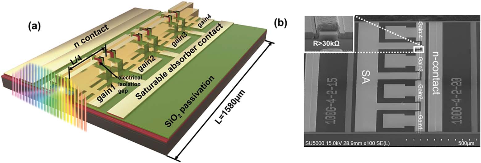
Fig. 1. (a) Schematic of InAs/GaAs fourth-order CPML design (total cavity length of 1580 μm) with four gain sections (360 μm for each section) and three equally spaced saturable absorbers (50 μm for each SA). (b) Cross-section SEM image of a fabricated device with a 45° tilted angle. Inset: magnified SEM image on electrical isolation trench region.
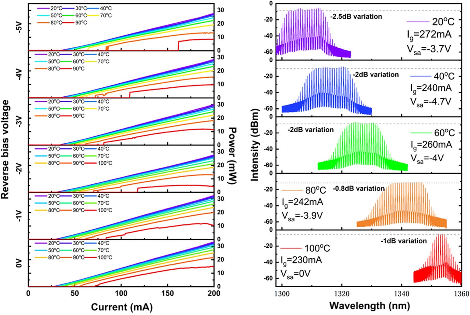
Fig. 2. (a) Temperature-dependent continuous-wave light current (L - I − 5 V L - I V SA
Fig. 3. Fourth-order QD-CPML. (a) Optical spectrum 3 dB bandwidth mapping as a function of SA reverse bias voltage ranging from 0 to 5 V with 0.5 V step and injection current of gain sections varying from 50 to 250 mA with 10 mA step. (b) A precisely swept map of comb line numbers within 3 dB optical bandwidth as a function of SA reverse bias voltage varying from 3 to 4.5 V with 0.1 V step and gain section injection current changing from 210 to 250 mA with 1 mA step [the mapping area corresponds to the red rectangular zone in (a)]. (c) Pulse width and (d) time–bandwidth product (TBP) mapping as a function of SA reverse bias voltage ranging from 0 to 5 V with 1 V step and gain section injection current ranging from 50 to 250 mA with 10 mA step. (e) Optical spectra and (f) pulse AC trace evolutions with injection current from 50 to 250 mA with 10 mA step at − 3 V
Fig. 4. (a) Optical spectrum of flat-top QD-CPML under optimized bias condition of I g = 224 mA V SA = − 3.8 V
Fig. 5. (a) Experimental setup used to measure B2B NRZ and PAM-4 transmission characteristics of QD-CPML, including ISO, optical isolator; OBPF, optical bandpass filter; PDFA, praseodymium-doped fiber amplifier; PC, polarization controller; AWG, arbitrary waveform generator; RF Amp, RF amplifier; MZM, Mach–Zehnder modulator; OSC, optical sampling oscilloscope. (b) 70 Gbit/s NRZ and (c) 40 GBaud PAM-4 optical eye diagram using comb line at 1321.28 nm.
Fig. 6. (a) Combined optical spectra of fourth-order QD-CPML for extended optical bandwidth under the temperatures of 15°C, 25°C, 51°C, and 63°C (purple line: I g = 195 mA V SA = − 2.8 V I g = 217 mA V SA = − 5 V I g = 240 mA V SA = − 3.3 V I g = 260 mA V SA = − 2.8 V
|
Table 1. Comparison of Mode-Locked Comb Laser on Various Material Platforms and Structures


Set citation alerts for the article
Please enter your email address

© Copyright 2018-2021 | Chinese Laser Press. All Rights Reserved 沪ICP备15018463号-20