
Tongchuan Ma, Xuanhu Chen, Fangfang Ren, Shunming Zhu, Shulin Gu, Rong Zhang, Youdou Zheng, Jiandong Ye. Heteroepitaxial growth of thick α-Ga2O3 film on sapphire (0001) by MIST-CVD technique[J]. Journal of Semiconductors, 2019, 40(1): 012804
- Journal of Semiconductors
- Vol. 40, Issue 1, 012804 (2019)
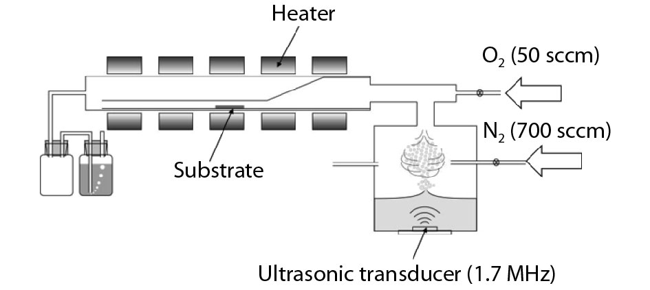
Fig. 1. Schematic illustration the mist-CVD system used for α -Ga2O3 epitaxy.
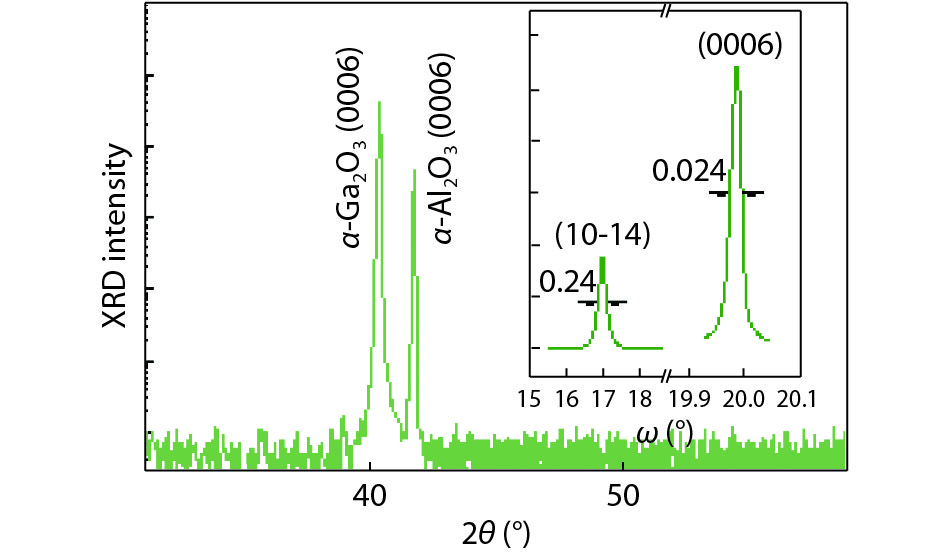
Fig. 2. (Color online) X-ray diffraction (XRD) 2θ /ω scan spectrum of the thick α -Ga2O3 epilayer. The inset displays the ω -scan rocking curves of (0006) and (10-14) planes under symmetric and skew-symmetric scan configuration, respectively.
Fig. 3. (Color online) XRD Φ -scan measurement for the (10-14) plane of the α -Ga2O3 epilayer and α -Al2O3 substrate.
Fig. 4. (Color online) (a) Optical microscopic image. (b) Large-scale atomic force microscopic image of the α -Ga2O3 epilayer. (c) Cross-sectional profile of grain. (d) AFM image of side facet of grain.
Fig. 5. (Color online) (a) The derived (αhv )1/2 curve as a function of photon energy and the inset displays the optical transmittance spectrum. (b) Raman scattering spectra of the α -Ga2O3 epilayer and α -Al2O3 substrate.

Set citation alerts for the article
Please enter your email address
© Copyright 2018-2021 | Chinese Laser Press. All Rights Reserved 沪ICP备15018463号-20