
Tongchuan Ma, Xuanhu Chen, Fangfang Ren, Shunming Zhu, Shulin Gu, Rong Zhang, Youdou Zheng, Jiandong Ye. Heteroepitaxial growth of thick α-Ga2O3 film on sapphire (0001) by MIST-CVD technique[J]. Journal of Semiconductors, 2019, 40(1): 012804
- Journal of Semiconductors
- Vol. 40, Issue 1, 012804 (2019)
Abstract
1. Introduction
Gallium oxide (Ga2O3), a representative ultra-wide bandgap (UWBG) semiconducting material, has attracted considerable attention in the applications of power electronic devices and solar-blind photodetectors owing to its unique properties, including an ultra-wide bandgap of about 4.9 eV and a high breakdown electric field of 8 MV/cm[
The growth of α-Ga2O3 thin films have been realized by various means of metal–organic vapor phase epitaxy (MOCVD)[
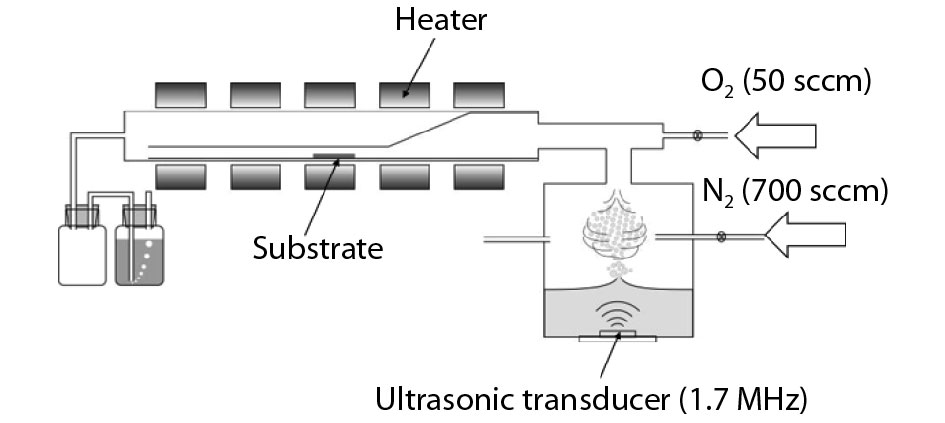
2. Experiment
The growth procedures were conducted using a hot-wall type mist-CVD system as developed by Shinohara and Fujita[
![]()
Figure 1.Schematic illustration the mist-CVD system used for
The microstructures of α-Ga2O3 epilayers were characterized by high resolution X-ray diffraction (HRXRD) using a D8 advance system with a Cu Kα X-ray source and a high resolution of 0.0001°. Optical transmission spectra were recorded by a UV-visible near-IR scanning spectrophotometer (Lambda 950, PerkinElmer). Raman scattering and photoluminescence spectroscopy measurements were performed at room temperature using a Micro-Raman spectrometer system (Horiba JY T64000) in a backscattering configuration with a 514 nm Ar+ laser as the excitation source. The laser was focused using a 100× objective for a spot size of ~2 μm in diameter and the excitation power was from 0.2 mW to avoid the laser heating effect. The surface morphology was investigated using atomic force microscopy (Asylum Research AFM).
3. Results and discussion
Fig. 2 shows the X-ray diffraction (XRD) 2θ/ω scan spectrum of the thick α-Ga2O3 epilayer. The spectrum is dominated by the diffraction peaks at 40.34° and 41.76°, which correspond to the (0006) planes of α-Ga2O3 epilayer and sapphire substrate, respectively. The calculated lattice constant along the c-axis is 13.40 Å, consistent with that of the other reported values for α-Ga2O3. There are no other distinct diffraction peaks observed in the XRD pattern, indicating phase-pure single crystalline α-Ga2O3 with (0001) out-of-plane orientation has been achieved. The inset of Fig. 2 illustrates the ω scan rocking curves of (0006) and (10-14) planes under symmetric and skew-symmetric scan configuration, respectively. The full-width at half maximum (FWHM) of the ω scan rocking curves for (0006) planes is as narrow as 0.024° (86 arcsec). Similar to the hexagonal III-nitride and ZnO epilayers grown on sapphire substrates, lattice twist and tilt are directly related to the dislocation density and can be roughly evaluated from the broadening feature of the ω scan[
![]()
Figure 2.(Color online) X-ray diffraction (XRD) 2
Fig. 3 shows the result of XRD Φ-scan measurement for the (10–14) plane of the α-Ga2O3 epilayer and α-Al2O3 substrate. Predominant peaks with 120° intervals appear at the same rotational angle of Φ, suggesting the epitaxial α-Ga2O3 film has the same corundum structure as the substrate. The epitaxial relationship is [0001]α-Ga2O3//[0001]α-Al2O3 in the out-of-plane orientation and [10-10]α-Ga2O3//[10-10]α-Al2O3 in the in-plane orientation. Aside from the distinct peaks of three-fold rotational symmetry, very weak peaks are seen in the α-Ga2O3 epilayer (marked by the red arrows in Fig. 3) at the positions rotated by 60° with respect to the predominant peaks. It means that a very small amount of 60°-twisted domains are formed during the epitaxial growth, which is expected to generate edge dislocations surrounding the twist boundaries of the rotational domains. The crystalline domains can be observed by the optical microscopic and atomic force microscopic (AFM) characterization as shown in Figs. 4(a) and 4(b), respectively. Determined from the optical microscopic image, the surface is crack-free but dominated by pyramid structures with different size distribution. The AFM image in Fig. 4(b) also clearly shows that a bunch of tetrahedron-structured grains dominates the surface morphology and the size of lateral coherent domain is in micron-scale. The cross-sectional profile of AFM shown in Fig. 4(c) shows that the angle between the side facet of the tetrahedron and the surface is about 6.05°, which is very close to the angle of 6.11° between the atomic planes of (0006) and (10-16). It indicates the side facets of tetrahedrons are in 10-16 orientation and exhibit a small roughness of 2.9 nm as shown in Fig. 4(d).
![]()
Figure 3.(Color online) XRD
![]()
Figure 4.(Color online) (a) Optical microscopic image. (b) Large-scale atomic force microscopic image of the
The optical transmittance spectrum of the α-Ga2O3 epilayer was recorded by using a c-plane sapphire substrate as reference and is shown in the inset of Fig. 5(a). A sharp absorption edge is observed at about 245 nm while the transmittance is low without the observable interference oscillations in the spectral range from near-ultraviolet to the visible region, which may suffer from a rough surface morphology. Typically, the optical bandgap can be evaluated by using the well-known Tauc rules of (αhν)n = A(hν − Eg), where the value of the exponent, n denotes the nature of the optical transitions[
Raman scattering is a powerful and nondestructive approach to probe lattice dynamics and evaluate crystalline quality and strain status. Fig. 5(b) shows the Raman scattering spectra of α-Ga2O3 epilayer obtained in a backscattering configuration together with that of α-Al2O3 substrate for reference. The Raman peaks located at 218.1, 288.4, 328.5, 431.4, 570.3, 690.3 cm−1 are the Raman-allowed vibration modes of A1g, Eg, Eg, Eg, Eg, A1g and Eg, respectively, consistent with the theoretical calculation in Ref. [27]. As reported by R. Cusco et al., the α-Ga2O3 with a rhombohedral structure belongs to the R3c space group and Raman active optical modes in the Brillouin zone center include 2A1g + 5Eg in terms of Raman selection rule. The low-frequency A1g mode at 218.1 cm−1 corresponds to Ga atoms vibrating against each other along the c-axis while the high-frequency A1g mode at 570.3 cm−1 mainly involves the vibration of oxygen atoms perpendicular to the c-axis. The linewidth of the low-frequency A1g is as narrow as 4.3 cm−1, strongly suggesting the highly crystallinity of the epilayer. As compared with the frequencies obtained from DFT calculations, the measured Raman frequencies are higher[
![]()
Figure 5.(Color online) (a) The derived (
4. Conclusion
In summary, the 8-μm thick single-crystalline crack-free α-Ga2O3 epilayers have been heteroepitaxially grown on sapphire (0001) substrates via the mist chemical vapor deposition technique. The resultant α-Ga2O3 has a low screw dislocation density of 2.24 × 106 cm−2 with very tiny lattice tilt from the (0006) orientation, while the 60°-twisted domains formed during the epitaxial growth leads to the generation of edge dislocations with a large density of about 1.63 × 109 cm−2. The surface is crack-free but dominated by pyramid structures with domain size in micron-scale. The optical transition exhibits an indirect nature with an optical bandgap of 5.03 eV. Lattice dynamics reveal the high crystallinity of the thick epilayer with a compressive residual strain not fully relaxed at the interface. The achieved high quality α-Ga2O3 with unique properties may be an alternative to β-Ga2O3 in the application of power devices and solar-blind photodetectors.
Acknowledgements
This work was supported by the National Key Research and Development Project (No. 2017YFB0403003), Shenzhen Fundamental Research Project (Nos. 201773239, 201888588), the National Natural Science Foundation of China (Nos. 61774081, 61322403), State Key Laboratory of Wide-Bandgap Semiconductor Power Electric Devices (No. 2017KF001), the Natural Science Foundation of Jiangsu Province (No. BK20161401), the Six Talent Peaks Project in Jiangsu Province (Mo. 2014XXRJ001), the Fundamental Research Funds for the Central Universities (Nos. 021014380093, 021014380085).
References
[1] J B Varley, J R Weber, A Janotti et al. Oxygen vacancies and donor impurities in
[2] M Higashiwaki, K Sasaki, A Kuramata et al. Gallium oxide (Ga2O3) metal–semiconductor field-effect transistors on single-crystal
[3] H Y Playford, A C Hannon, E R Barney et al. Structures of uncharacterised polymorphs of gallium oxide from total neutron diffraction. Chemistry, 19, 2803(2013).
[4] R Roy, V G Hill, E F Osborn. Polymorphism of Ga2O3 and the System Ga2O3–H2O. J Am Chem Soc, 74, 719(1952).
[5] H Aida, K Nishiguchi, H Takeda et al. Growth of
[6] W E Mahmoud. Solar blind avalanche photodetector based on the cation exchange growth of
[7] D Y Guo, H Z Shi, Y P Qian et al. Fabrication of
[8] X Zhao, Z Wu, D Guo et al. Growth and characterization of
[9] X Chen, Y Xu, D Zhou et al. Solar-blind photodetector with high avalanche gains and bias-tunable detecting functionality based on metastable phase alpha-Ga2O3/ZnO isotype heterostructures. ACS Appl Mater Interfaces, 9, 36997(2017).
[10] J Li, X Chen, T Ma et al. Identification and modulation of electronic band structures of single-phase
[11] B Zhao, F Wang, H Chen et al. Solar-blind avalanche photodetector based on single ZnO–Ga2O3 core-shell microwire. Nano Lett, 15, 3988(2015).
[12] K Sasaki, M Higashiwaki, A Kuramata et al. Ga2O3 Schottky barrier diodes fabricated by using single-crystal
[13] K Akaiwa, S Fujita. Electrical conductive corundum-structured
[14] H Ito, K Kaneko, S Fujita. Growth and band gap control of corundum-structured
[15] K Kaneko, T Nomura, I Kakeya et al. Fabrication of highly crystalline corundum-structured
[16] H Sun, K H Li, C G T Castanedo et al. HCl flow-induced phase change of
[17] Y Yao, S Okur, L A M Lyle et al. Growth and characterization of
[18] R Kumaran, T Tiedje, S E Webster et al. Epitaxial Nd-doped alpha-(Al(1−
[19] S Fujita, M Oda, K Kaneko et al. Evolution of corundum-structured III-oxide semiconductors: Growth, properties, and devices. Jpn J Appl Phys, 55, 1202A3(2016).
[20] M Oda, K Kaneko, S Fujita et al. Crack-free thick (~5
[21] D Shinohara, S Fujita. Heteroepitaxy of corundum-structured
[22] T Kawaharamura. Physics on development of open-air atmospheric pressure thin film fabrication technique using mist droplets: Control of precursor flow. Jpn J Appl Phys, 53, 05FF08(2014).
[23] M A Moram, M E Vickers. X-ray diffraction of III-nitrides. Rep Prog Phys, 72, 036502(2009).
[24] X H Zheng, H Chen, Z B Yan et al. Determination of twist angle of in-plane mosaic spread of GaN films by high-resolution X-ray diffraction. J Cryst Growth, 255, 63(2003).
[25] K Kaneko, H Kawanowa, H Ito et al. Evaluation of misfit relaxation in
[26] E A Davis, N F Mott et al. Conduction in non-crystalline systems V. Conductivity, optical absorption and photoconductivity in amorphous semiconductors. Philos Mag A, 22, 0903(1970).
[27] R Cusco, N Domenech-Amador, T Hatakeyama et al. Lattice dynamics of a mist-chemical vapor deposition-grown corundum-like Ga2O3 single crystal. J Appl Phys, 117, 185706(2015).

Set citation alerts for the article
Please enter your email address
© Copyright 2018-2021 | Chinese Laser Press. All Rights Reserved 沪ICP备15018463号-20