• Photonics Research
  • Vol. 9, Issue 3, 299 (2021)
A. Kafar1、2、*, A. Sakaki3, R. Ishii1, S. Stanczyk2、4, K. Gibasiewicz2, Y. Matsuda1, D. Schiavon2、4, S. Grzanka2、4, T. Suski2, P. Perlin2、4, M. Funato1, and Y. Kawakami1
Author Affiliations
  • 1Department of Electronic Science and Engineering, Kyoto University, Kyoto 615-8510, Japan
  • 2Institute of High Pressure Physics PAS, Sokolowska 29/37, 01-142 Warsaw, Poland
  • 3Nichia Corporation, Anan, Tokushima 774-8601, Japan
  • 4TopGaN Ltd., Sokolowska 29/37, 01-142 Warsaw, Poland
  • show less
    DOI: 10.1364/PRJ.411701 Cite this Article Set citation alerts
    A. Kafar, A. Sakaki, R. Ishii, S. Stanczyk, K. Gibasiewicz, Y. Matsuda, D. Schiavon, S. Grzanka, T. Suski, P. Perlin, M. Funato, Y. Kawakami. Influence of substrate misorientation on the emission and waveguiding properties of a blue (In,Al,Ga)N laser-like structure studied by synchrotron radiation microbeam X-ray diffraction[J]. Photonics Research, 2021, 9(3): 299 Copy Citation Text show less
    3D shape of the examined area with misorientation change and the corresponding misorientation map of this area. The dotted line presents the orientation of the synchrotron XRD scan, with the direction from A to B.
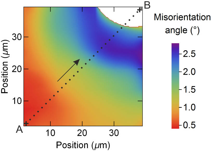
    Fig. 1. 3D shape of the examined area with misorientation change and the corresponding misorientation map of this area. The dotted line presents the orientation of the synchrotron XRD scan, with the direction from A to B.
    Map of the peak emission wavelength of the area studied in this experiment. The map was measured with excitation power density of around 0.2 kW/cm2. The dotted line presents the orientation of the synchrotron XRD scan, with the direction from A to B.
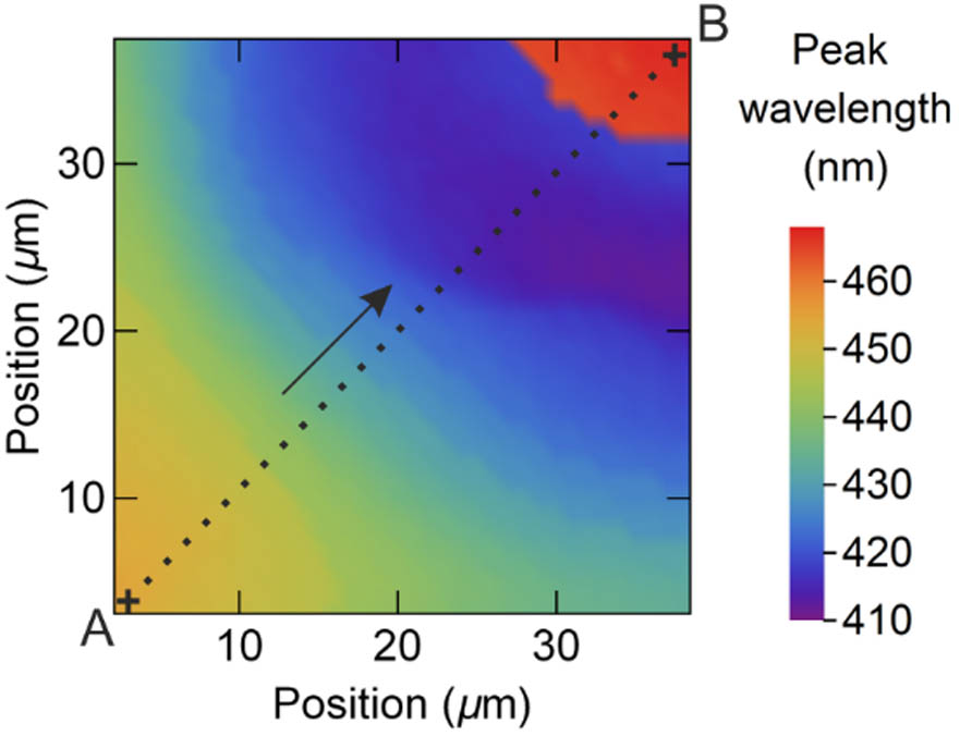
    Fig. 2. Map of the peak emission wavelength of the area studied in this experiment. The map was measured with excitation power density of around 0.2  kW/cm2. The dotted line presents the orientation of the synchrotron XRD scan, with the direction from A to B.
    Set of the XRD scans obtained along the diagonal of the test area, from point A to point B as marked in Figs. 1 and 2. A clear shift of the InGaN-related peak is observed. For clarity, the intensity scans were shifted vertically.
    Fig. 3. Set of the XRD scans obtained along the diagonal of the test area, from point A to point B as marked in Figs. 1 and 2. A clear shift of the InGaN-related peak is observed. For clarity, the intensity scans were shifted vertically.
    Parameters of the quantum wells obtained through SR-XRD scan: (a) indium content and (b) layer thickness. The (a) plot includes also μPL peak wavelength profile based on the data presented in Fig. 2. Position 0 corresponds to point A in Figs. 1 and 2.
    Fig. 4. Parameters of the quantum wells obtained through SR-XRD scan: (a) indium content and (b) layer thickness. The (a) plot includes also μPL peak wavelength profile based on the data presented in Fig. 2. Position 0 corresponds to point A in Figs. 1 and 2.
    Estimation of the Stokes shift of the PL emission based on comparison with the simulated transition energy. (a) The dependence of the emission energy versus position was estimated as a first-order interpolation of the experimental data and subtracted from the calculated transition energy. (b) The obtained difference was presented as a dependence on local In content and fitted with a linear function, which is used as the Stokes shift estimation.
    Fig. 5. Estimation of the Stokes shift of the PL emission based on comparison with the simulated transition energy. (a) The dependence of the emission energy versus position was estimated as a first-order interpolation of the experimental data and subtracted from the calculated transition energy. (b) The obtained difference was presented as a dependence on local In content and fitted with a linear function, which is used as the Stokes shift estimation.
    Relation of the μPL peak wavelength and the In content measured by SR-XRD compared with the values obtained through simulation of transition energy for the ground states of a single QW in the presence of electric fields. The transition energy was calculated based on the local parameters obtained from XRD and corrected using the In-content-dependent Stokes shift estimated in Fig. 5. The continuous line is a guide to the eye.
    Fig. 6. Relation of the μPL peak wavelength and the In content measured by SR-XRD compared with the values obtained through simulation of transition energy for the ground states of a single QW in the presence of electric fields. The transition energy was calculated based on the local parameters obtained from XRD and corrected using the In-content-dependent Stokes shift estimated in Fig. 5. The continuous line is a guide to the eye.
    Comparison of the spatial relation between the local misorientation angle and indium content in the quantum wells measured through SR-XRD: (a) as a dependence on position and (b) estimated relation of both types of values.
    Fig. 7. Comparison of the spatial relation between the local misorientation angle and indium content in the quantum wells measured through SR-XRD: (a) as a dependence on position and (b) estimated relation of both types of values.
    Parameters of the InGaN layer obtained through SR-XRD scan: (a) indium content and (b) layer thickness. Position 0 corresponds to point A in Figs. 1 and 2.
    Fig. 8. Parameters of the InGaN layer obtained through SR-XRD scan: (a) indium content and (b) layer thickness. Position 0 corresponds to point A in Figs. 1 and 2.
    Parameters of the AlGaN layer obtained through SR-XRD scan: (a) aluminum content and (b) layer thickness. Position 0 corresponds to point A in Figs. 1 and 2.
    Fig. 9. Parameters of the AlGaN layer obtained through SR-XRD scan: (a) aluminum content and (b) layer thickness. Position 0 corresponds to point A in Figs. 1 and 2.
    Relation between the composition of layers imitating InGaN waveguide and AlGaN cladding and the local misorientation angle of the sample. The continuous lines are guides to the eye.
    Fig. 10. Relation between the composition of layers imitating InGaN waveguide and AlGaN cladding and the local misorientation angle of the sample. The continuous lines are guides to the eye.
    Comparison of the calculated optical confinement factor Γ of the structure with other parameters as a dependence on position on the diagonal of the square pattern: (a) quantum well thickness and In content, and (b) confinement factor and local substrate misorientation. In (b), we present the optimally calculated confinement factor by crosses (based on the PL wavelength under high excitation). Additional data, depicted by diamond markers, refer to the same structural parameters as crosses but calculated for the propagating light characterized by 439.8 nm wavelength value obtained for P3.
    Fig. 11. Comparison of the calculated optical confinement factor Γ of the structure with other parameters as a dependence on position on the diagonal of the square pattern: (a) quantum well thickness and In content, and (b) confinement factor and local substrate misorientation. In (b), we present the optimally calculated confinement factor by crosses (based on the PL wavelength under high excitation). Additional data, depicted by diamond markers, refer to the same structural parameters as crosses but calculated for the propagating light characterized by 439.8 nm wavelength value obtained for P3.
    Comparison of the optical mode profiles of the structure calculated based on data estimated for points P1 (position 38 μm) and P4 (position 15 μm, maximal confinement factor). The black and gray lines present the refractive index profiles for the two points.
    Fig. 12. Comparison of the optical mode profiles of the structure calculated based on data estimated for points P1 (position 38 μm) and P4 (position 15 μm, maximal confinement factor). The black and gray lines present the refractive index profiles for the two points.
    LayerThickness (nm)Type
    GaN32
    In0.14GaN2.1QW
    GaN6.5
    In0.14GaN2.1QW
    GaN6.5
    In0.04GaN:Si50Waveguide
    GaN:Si10
    Al0.040GaN:Si100
    Al0.04GaN:Si100Cladding
    GaN:Si500
    GaN substrate
    Table 1. Structure of the Examined Samplea
    Al or In Content
     Position (μm)AlGaN Cladding TopAlGaN EBLInGaN Waveguide TopInGaN QWInGaN Waveguide BottomAlGaN Cladding BottomλPL (nm)
    P100.0490.1170.0430.1840.0430.073445.8
    P270.0500.1200.0400.1720.0400.075446.4
    P3150.0490.1180.0340.1490.0340.074439.8
    P4230.0470.1120.0260.1220.0260.070427.4
    P5290.0450.1070.0220.1060.0220.067420.1
    P6380.0420.1010.0190.0950.0190.063412.4
    Thickness (nm)
     Position (μm)AlGaN Cladding TopAlGaN EBLInGaN Waveguide TopInGaN QWInGaN Waveguide BottomAlGaN Cladding Bottom
    P1057921.159.21.945.5843
    P2755020.065.02.250.0800
    P31554319.769.92.353.8789
    P42356320.573.02.456.2819
    P52959721.774.12.457.0869
    P63867824.673.92.356.8986
    Table 2. Parameters Used for the Simulation of the Optical Confinement Factor in a Full Laser Structure
    A. Kafar, A. Sakaki, R. Ishii, S. Stanczyk, K. Gibasiewicz, Y. Matsuda, D. Schiavon, S. Grzanka, T. Suski, P. Perlin, M. Funato, Y. Kawakami. Influence of substrate misorientation on the emission and waveguiding properties of a blue (In,Al,Ga)N laser-like structure studied by synchrotron radiation microbeam X-ray diffraction[J]. Photonics Research, 2021, 9(3): 299
    Download Citation