A. Kafar1,2,*, A. Sakaki3, R. Ishii1, S. Stanczyk2,4..., K. Gibasiewicz2, Y. Matsuda1, D. Schiavon2,4, S. Grzanka2,4, T. Suski2, P. Perlin2,4, M. Funato1 and Y. Kawakami1|Show fewer author(s)
A. Kafar, A. Sakaki, R. Ishii, S. Stanczyk, K. Gibasiewicz, Y. Matsuda, D. Schiavon, S. Grzanka, T. Suski, P. Perlin, M. Funato, Y. Kawakami, "Influence of substrate misorientation on the emission and waveguiding properties of a blue (In,Al,Ga)N laser-like structure studied by synchrotron radiation microbeam X-ray diffraction," Photonics Res. 9, 299 (2021)
Copy Citation Text
In this work, we study how an epitaxial laser-like (or superluminescent diode-like) structure is modified by intentional changes of the substrate misorientation in the range of 0.5°–2.6°. The μμ test structure with misorientation profiling was fabricated using multilevel photolithography and dry-etching. The local structural parameters were measured by synchrotron radiation microbeam X-ray diffraction, with the sampling area of below μμ. We directly obtained the relation between the misorientation and indium content in the quantum well, changing from 9% to 18%, with a high resolution (small misorientation step). We also show a good agreement of local photoluminescence emission wavelength with simulation of transition energy based on synchrotron radiation microbeam X-ray diffraction (SR-XRD) data and estimated Stokes shift. We observe that the substrate misorientation influences also the InGaN waveguide and AlGaN cladding composition. Still, we showed through simulation of the optical confinement factor of a full laser diode structure that good light guiding properties should be preserved in the whole misorientation range studied here. This proves the usefulness of misorientation modification in applications like broadband superluminescent diodes or multicolor laser arrays.
1. INTRODUCTION
Nitride light emitters have quickly evolved from first demonstrations [1–3] to commercial products [4–8] and become the part of our everyday life, and their presence is still expanding as new applications are explored [9–11]. The vast range of developments includes high optical power and efficiency [12,13], a wide choice of emission wavelength [14–17], or new functionalities [10,18,19]. One of the important aspects of a state-of-the-art device is its high crystalline quality of the structure. The morphology of the grown layers strongly depends on the epitaxial growth mode [20,21], and it is usually preferred to ensure a step-flow mode. Typically, a vicinal substrate (surface plane misoriented with respect to the atomic planes) helps in achieving a step-flow growth [22–25]. Substrate misorientation can be formed by mechanochemical polishing [26,27], which allows the formation of a smooth and defect-free surface. In the case of bulk GaN substrates, usually a moderate misorientation of 0.3°–0.6° is used. It was demonstrated that, in the case of high indium content layers grown at lowered temperatures, the increase of substrate misorientation can make a dramatic change in the layer morphology [28].
It is important to note that increasing the misorientation of the substrate can influence not only morphology. It was reported that such changes can increase the hole concentration in Mg-doped p-GaN [29] and reduce the carbon impurity incorporation [30]. On the other hand, in the case of InGaN layers, a change of In incorporation with increasing misorientation angle was revealed [31–33]. It was also demonstrated that by proper patterning of the substrate, areas of different misorientation values can be created. This enables fabrication of multicolor devices [34,35] or broadening of superluminescent diode emission spectra [36,37]. While developing the latter solution, in our previous work [38] we studied how the InGaN quantum well (QW) emission properties are modified with the changes of misorientation. We demonstrated that it is possible to obtain, during the same growth procedure, a change of the central emission wavelength of above 25 nm in the blue–violet region with a wide range of misorientation where the light intensity is rather constant.
The goal of this study is to examine in more detail how the substrate misorientation angle influences the structural parameters of the epitaxial layers (a design including layers imitating waveguide and cladding layers below the active region). Thanks to the use of synchrotron radiation microbeam X-ray diffraction (SR-XRD), we were able to study the whole structure along a misorientation profile in a range of around 0.5° to 2.8°. We directly demonstrate the relation between the misorientation and In content in the QWs as well as the photoluminescence (PL) emission wavelength and In content. Good agreement of the calculated transition energy with the experimental PL results confirms the SR-XRD result that for lowest misorientation angles the QW thickness is reduced. Interestingly, not only InGaN but also the AlGaN layer shows a modification by substrate misorientation. This is an interesting conclusion not only from the point of view of special emitters like broadband superluminescent diodes, but also standard laser diodes as it shows that the same growth procedure may give different optoelectrical parameters of the device when it is grown on different substrates.
Sign up for Photonics Research TOC. Get the latest issue of Photonics Research delivered right to you!Sign up now
2. FABRICATION AND EXPERIMENTAL METHODS
The epitaxial structure studied within this measurement was grown on a patterned c-plane bulk GaN substrate, which included areas with changing misorientation angle. The details of the fabrication procedure are presented in our previous work [38] and include multilevel photolithography and dry-etching steps that allow us to obtain 3D shapes on the substrate surface. For this study, we chose a pattern with a non-linear misorientation profile that makes it easier to study the areas with lowest and highest substrate misorientation. After the substrate was prepared, we performed metal organic vapor phase epitaxy (MOVPE) of a structure, which simulates the bottom part of a laser diode or superluminescent diode and its active region; however, the AlGaN cladding layers were thinner than in a real structure. The active region consisted of two InGaN QWs surrounded by GaN barriers. The intentional structure, optimized for growth on around 0.5° misoriented substrate, is presented in Table 1.
Structure of the Examined Samplea
Layer
Thickness (nm)
Type
GaN
32
2.1
QW
GaN
6.5
2.1
QW
GaN
6.5
50
Waveguide
GaN:Si
10
100
100
Cladding
GaN:Si
500
GaN substrate
Below the active region, layers imitating InGaN waveguide and AlGaN cladding of typical edge emitters are included.
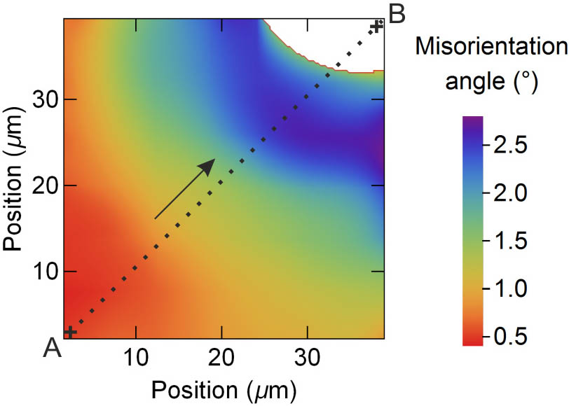
Figure 1.3D shape of the examined area with misorientation change and the corresponding misorientation map of this area. The dotted line presents the orientation of the synchrotron XRD scan, with the direction from A to B.
Figure 2.Map of the peak emission wavelength of the area studied in this experiment. The map was measured with excitation power density of around . The dotted line presents the orientation of the synchrotron XRD scan, with the direction from A to B.
Figure 3.Set of the XRD scans obtained along the diagonal of the test area, from point A to point B as marked in Figs. 1 and 2. A clear shift of the InGaN-related peak is observed. For clarity, the intensity scans were shifted vertically.
Figure 4.Parameters of the quantum wells obtained through SR-XRD scan: (a) indium content and (b) layer thickness. The (a) plot includes also μPL peak wavelength profile based on the data presented in Fig. 2. Position 0 corresponds to point A in Figs. 1 and 2.
Figure 5.Estimation of the Stokes shift of the PL emission based on comparison with the simulated transition energy. (a) The dependence of the emission energy versus position was estimated as a first-order interpolation of the experimental data and subtracted from the calculated transition energy. (b) The obtained difference was presented as a dependence on local In content and fitted with a linear function, which is used as the Stokes shift estimation.
Figure 6.Relation of the μPL peak wavelength and the In content measured by SR-XRD compared with the values obtained through simulation of transition energy for the ground states of a single QW in the presence of electric fields. The transition energy was calculated based on the local parameters obtained from XRD and corrected using the In-content-dependent Stokes shift estimated in Fig. 5. The continuous line is a guide to the eye.
Figure 7.Comparison of the spatial relation between the local misorientation angle and indium content in the quantum wells measured through SR-XRD: (a) as a dependence on position and (b) estimated relation of both types of values.
4. MODIFICATION OF WAVEGUIDE AND CLADDING PROPERTIES
The results presented to this point clearly demonstrate that the In content is closely following the change of the local misorientation of the substrate. Although such relation was already reported, our current experiment allowed us to directly compare the same positions of the sample by both PL and SR-XRD. Also, it can be safely assumed that the growth conditions (pressure, temperature, etc.) were the same during the growth of all the studied points, as the distance between the farthest studied points is below 55 μm.
Figure 8.Parameters of the InGaN layer obtained through SR-XRD scan: (a) indium content and (b) layer thickness. Position 0 corresponds to point A in Figs. 1 and 2.
Figure 9.Parameters of the AlGaN layer obtained through SR-XRD scan: (a) aluminum content and (b) layer thickness. Position 0 corresponds to point A in Figs. 1 and 2.
Figure 10.Relation between the composition of layers imitating InGaN waveguide and AlGaN cladding and the local misorientation angle of the sample. The continuous lines are guides to the eye.
To check how the change of substrate misorientation may affect the performance of real laser diodes or superluminescent diodes, we carried out a simulation based on a standard graded index separate confinement heterostructure introduced in Ref. [46] using the SiLENSe software, for sets of layer composition and thickness data obtained through this experiment. To reduce the scatter, we first fitted the data presented in Figs. 4, 8, and 9 with low-degree polynomials. Next, we chose six positions (P1–P6) that reflected the full range of In or Al content changes of sample parameters. As our test structure, shown in Table 1, has different values of the thicknesses from a real waveguide and cladding layers, we estimated the width proportionally to the changes in the current sample assuming that the structure measured for P3 corresponds to a standard structure on a non-patterned sample. The full list of parameters that were changed during the simulation is presented in Table 2. Other parameters are assumed as presented in Ref. [46]. The wavelength of light used for the mode simulation was assumed based on the PL mapping results. The data used for this calculation are extracted from the diagonal of a map analogous to what is presented in Fig. 2, but measured at higher excitation of around , which is closer to the work conditions (high carrier density) of the edge-emitting devices.
Parameters Used for the Simulation of the Optical Confinement Factor in a Full Laser Structure
Al or In Content
Position (μm)
AlGaN Cladding Top
AlGaN EBL
InGaN Waveguide Top
InGaN QW
InGaN Waveguide Bottom
AlGaN Cladding Bottom
(nm)
P1
0
0.049
0.117
0.043
0.184
0.043
0.073
445.8
P2
7
0.050
0.120
0.040
0.172
0.040
0.075
446.4
P3
15
0.049
0.118
0.034
0.149
0.034
0.074
439.8
P4
23
0.047
0.112
0.026
0.122
0.026
0.070
427.4
P5
29
0.045
0.107
0.022
0.106
0.022
0.067
420.1
P6
38
0.042
0.101
0.019
0.095
0.019
0.063
412.4
Thickness (nm)
Position (μm)
AlGaN Cladding Top
AlGaN EBL
InGaN Waveguide Top
InGaN QW
InGaN Waveguide Bottom
AlGaN Cladding Bottom
P1
0
579
21.1
59.2
1.9
45.5
843
P2
7
550
20.0
65.0
2.2
50.0
800
P3
15
543
19.7
69.9
2.3
53.8
789
P4
23
563
20.5
73.0
2.4
56.2
819
P5
29
597
21.7
74.1
2.4
57.0
869
P6
38
678
24.6
73.9
2.3
56.8
986
Figure 11.Comparison of the calculated optical confinement factor of the structure with other parameters as a dependence on position on the diagonal of the square pattern: (a) quantum well thickness and In content, and (b) confinement factor and local substrate misorientation. In (b), we present the optimally calculated confinement factor by crosses (based on the PL wavelength under high excitation). Additional data, depicted by diamond markers, refer to the same structural parameters as crosses but calculated for the propagating light characterized by 439.8 nm wavelength value obtained for P3.
Figure 12.Comparison of the optical mode profiles of the structure calculated based on data estimated for points P1 (position 38 μm) and P4 (position 15 μm, maximal confinement factor). The black and gray lines present the refractive index profiles for the two points.
Within this work, we studied the properties of a nitride structure grown on an area with profiled misorientation. The experiment is based on the SR-XRD with the beam size of below μμ, allowing us to examine the sample with very high resolution. The sample included two InGaN QWs and, below, a set of layers imitating the laser diode or superluminescent diode structure: an InGaN waveguide layer and an AlGaN cladding layer. The results were compared with the data obtained from μPL mapping allowing us to show the relation between the emission wavelength and In content of the QWs in the area of changing misorientation. We observed a change of In content in a range of around 9% to 18% and proved that the shift of emission is not induced by a change of QW thickness. We were also able to reproduce the PL emission wavelength value simulating the transition energy of a QW characterized by parameters obtained through the XRD measurements. Additionally, we observed that the misorientation influences also the other layers of the structure. Both the InGaN waveguide and the AlGaN cladding seem to show a change of composition (decrease of In or Al content) with increasing misorientation. This result has important practical consequences, showing that intentionally the same epitaxial structure may change its properties significantly when it is fabricated on substrates with different misorientation. To examine this effect more explicitly, we performed simulations of full laser diode structures. We observe that although the optical confinement factor is changed when moving away from the misorientation for which the structure is optimized, the variation is rather small. This is probably thanks to both the increase of layer thickness for the regions of lowered In or Al content, as well as the wavelength dependence of the refractive index of the layers. Our results show that the usage of the substrate misorientation change does not lead to a serious structural quality deterioration and that the method is a practical approach for device fabrication.
Acknowledgment
Acknowledgment. The synchrotron radiation experiments were performed with the approval of the Japan Synchrotron Radiation Research Institute (JASRI) (Proposal Nos. 2019B5080 and 2020A5082).
[8] M. Kawaguchi, O. Imafuji, S. Nozaki, H. Hagino, K. Nakamura, S. Takigawa, T. Katayama, T. Tanaka. Record-breaking high-power InGaN-based laser-diodes using novel thick-waveguide structure. International Semiconductor Laser Conference (ISLC), 1-2(2016).
[41] M. Hayakawa, Y. Hayashi, S. Ichikawa, M. Funato, Y. Kawakami. Enhanced radiative recombination probability in AlGaN quantum wires on (0001) vicinal surface. Proc. SPIE, 9926, 99260S(2016).
A. Kafar, A. Sakaki, R. Ishii, S. Stanczyk, K. Gibasiewicz, Y. Matsuda, D. Schiavon, S. Grzanka, T. Suski, P. Perlin, M. Funato, Y. Kawakami, "Influence of substrate misorientation on the emission and waveguiding properties of a blue (In,Al,Ga)N laser-like structure studied by synchrotron radiation microbeam X-ray diffraction," Photonics Res. 9, 299 (2021)