
Tingwei Lu, Xiangshu Lin, Wenan Guo, Chang-Ching Tu, Shibiao Liu, Chun-Jung Lin, Zhong Chen, Hao-Chung Kuo, Tingzhu Wu. High-speed visible light communication based on micro-LED: A technology with wide applications in next generation communication[J]. Opto-Electronic Science, 2022, 1(12): 220020
- Opto-Electronic Science
- Vol. 1, Issue 12, 220020 (2022)
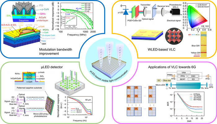
Fig. 1. Summary of the review, which includes modulation bandwidth improvement, white light emitting diodes (WLED)-based visible light communication (VLC), micro light emitting diode (μLED) detector and applications of VLC towards 6G. Figure reproduced from: ref.96, 125, 154, 165, American Chemical Society; ref.139, 153, Chinese Laser Press; ref.161, 166, OSA Open Access Publishing Agreement; ref.175, 184, Optical Society of America.
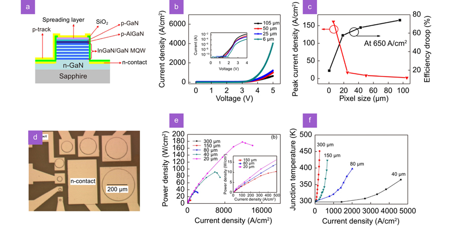
Fig. 2. (a ) Schematic of the samples’ structure. (b ) J–V characteristics of samples. (c ) Current densities of peak EQE, and the efficiency drop of samples. (d ) Optical micrograph. (e ) Power density and (f ) junction temperature of the samples at different current densities. Figure reproduced with permission from: (a–c) ref.61, AIP Publishing; (d–f) ref.64, AIP Publishing.
Fig. 3. (a ) Transmission electron microscopy (TEM) image. (b ) Three-dimensional schematic and (c ) scanning electron microscopy (SEM) image of a µLED. (d ) −3 dB bandwidth for different current densities. Schematics of fabrication for the growth of μLEDs on a high-electron-mobility transistor (HEMT) template. (e ) Deposition of SiO2. (f ) Fabrication of SiO2 microhole arrays. (g ) Growth of μLEDs. (h ) SiO2 mask removal. (i ) Modulation bandwidth and (j ) electroluminescence (EL) spectra of device. Figure reproduced with permission from: (a–d) ref.90, IEEE; (e–j) ref.100, under a Creative Commons Attribution (CC-BY) License.
Fig. 4. (a ) Bandwidth for devices with different crystal orientations. (b ) Schematic and (c ) frequency response of the nonpolar μLED. (d ) Schematic diagram of semipolar (20–21) green μLED structures. (e ) Time-resolved photoluminescence (TRPL) curves of semipolar μLED and c-plane μLED. (f ) Frequency response of the semipolar μLED. (g ) PR and (h ) frequency responses of μLED array. (i ) BER and signal-to-noise ratio at 4.5 Gbit/s transmission rate with different sampling rates. Figure reproduced with permission from: (a) ref.65, AIP Publishing; (b, c) ref.103, IEEE; (d–f) ref.96, American Chemical Society; (g–i) ref.109, Optica Publishing Group.
Fig. 5. (a ) Schematic. (b ) HRTEM image of the QWs. (c ) Bandwidth of single chip WLED vs. injection current density. (d ) Eye diagram at transmission rate of 50 and 127 Mbps. (e ) TEM images of InGaN QDs. (f ) –3 dB bandwidth and (g ) BER at different current densities. Figure reproduced with permission from: (a–d) ref.118, Optica Publishing Group; (e–g) ref.91, ACS Publishing.
Fig. 6. SEM images of the nanowires after (a ) QW and (b ) p-GaN growth and (c ) the fully fabricated nanowire μLED device. (d ) −3 dB bandwidth of device. (e ) TRPL of PLED and control LED. Figure reproduced with permission from: (a–d) ref.125, American Chemical Society; (e) ref.129, American Chemical Society.
Fig. 7. (a ) Schematic diagram of WLED device based on semipolar μLED array. (b ) Photographs of the μLED array without current. (c ) Spectrum of the WLED. (d ) Measured normalized frequency response of μLED array. (e ) BER curve of the white-light VLC system. Figure reproduced with permission from: (a–e) ref.87, under the Optica Open Access Publishing Agreement.
Fig. 8. (a ) White-light VLC system consisting of perovskite quantum dot (PQD) and blue μLED. (b ) The longevity of the PL properties of the PNCs. (c ) Frequency response of the PNC-μLED. (d ) TRPL measurement for semipolar μLED, PQD and CdSe QD papers. (e ) Frequency response of PQD paper and PQD film. (f ) TEM images of RQDs. (g ) TRPL measurement for YQDs and RQDs. (h ) Frequency response of red and yellow PNC-PMMA. Figure reproduced with permission from: (a) ref.152, American Chemical Society; (b, c) ref.139, American Chemical Society; (d, e) ref.153, Optica Publishing Group; (f–h) ref.154, American Chemical Society.
Fig. 9. (a ) Composition of WLED active region. (b ) The distribution analysis of In components in QWs. (c ) Modulation bandwidths of different sizes µLEDs. (d ) Power spectra of OFDM-modulated waveforms measured at data rates of 4.42 Gbps, 3.72 Gbps, and 336 Mbps. (e ) Constellations under corresponding order QAM modulation. Figure reproduced with permission from: (a–c) ref.161, under the OSA Open Access Publishing Agreement; (d, e) ref.162, under a Creative Commons Attribution (CC-BY) License.
Fig. 10. (a ) Cross-section of the μLED and schematic setup for VLC system using the μLED based photodetectors. (b ) Current–voltage (I–V) curves of the μLED-based PD with diameters of 60 μm under darkness and illumination. (c ) Responsivities of the μLED-based PD measured for various laser wavelengths. (d ) Frequency response for μLED-based PD. (e ) Eye diagrams at a transmission rate of 160 Mbps. (f ) Cross-section of semipolar green μLEDs. (g ) Frequency responses of μLED PD. (h ) BERs with μLEDs as PD at a transmission rate of 540 Mbps. Figure reproduced with permission from: (a–e) ref.165, American Chemical Society; (f–h) ref.166, under the OSA Open Access Publishing Agreement.
Fig. 11. (a ) Schematic of setup and (b ) photograph and (c ) frequency responses of the μLED-based UOWC system. (d ) Light output power (LOP) and forward current characteristics of the μLED-on-HEMT arrays. Figure reproduced with permission from: (a–c) ref.175, under a Creative Commons Attribution license; (d) ref.176, under a Creative Commons Attribution License.
Fig. 12. (a ) Schematic of the VLC system based on μLED and ANN equalizers. (b ) Schematic of the arrangement of pilots. (c ) BER in simulation with different pilot lengths. BER performance for (d ) 50- and (e ) 75-µm blue μLEDs. Figure reproduced with permission from ref.184, Optical Society of America.
|
Table 1. Summary of research progress in the VLC system based on μLED


Set citation alerts for the article
Please enter your email address

© Copyright 2018-2021 | Chinese Laser Press. All Rights Reserved 沪ICP备15018463号-20