Abstract
The evolution of next-generation cellular networks is aimed at creating faster, more reliable solutions. Both the next-generation 6G network and the metaverse require high transmission speeds. Visible light communication (VLC) is deemed an important ancillary technology to wireless communication. It has shown potential for a wide range of applications in next-generation communication. Micro light-emitting diodes (μLEDs) are ideal light sources for high-speed VLC, owing to their high modulation bandwidths. In this review, an overview of μLEDs for VLC is presented. Methods to improve the modulation bandwidth are discussed in terms of epitaxy optimization, crystal orientation, and active region structure. Moreover, electroluminescent white LEDs, photoluminescent white LEDs based on phosphor or quantum-dot color conversion, and μLED-based detectors for VLC are introduced. Finally, the latest high-speed VLC applications and the application prospects of VLC in 6G are introduced, including underwater VLC and artificial intelligence-based VLC systems.The evolution of next-generation cellular networks is aimed at creating faster, more reliable solutions. Both the next-generation 6G network and the metaverse require high transmission speeds. Visible light communication (VLC) is deemed an important ancillary technology to wireless communication. It has shown potential for a wide range of applications in next-generation communication. Micro light-emitting diodes (μLEDs) are ideal light sources for high-speed VLC, owing to their high modulation bandwidths. In this review, an overview of μLEDs for VLC is presented. Methods to improve the modulation bandwidth are discussed in terms of epitaxy optimization, crystal orientation, and active region structure. Moreover, electroluminescent white LEDs, photoluminescent white LEDs based on phosphor or quantum-dot color conversion, and μLED-based detectors for VLC are introduced. Finally, the latest high-speed VLC applications and the application prospects of VLC in 6G are introduced, including underwater VLC and artificial intelligence-based VLC systems.Introduction
Innovations in smartphones and smart homes, and the emergence of online services have propelled the growth of cloud computing, the Internet of Things, and autonomous driving1-6. In the future, the metaverse, a fledgling networking technology, will allow users to experience multimedia by combining distributed real-time sources and stored digital assets in real time. However, its real-time interactive nature will significantly increase requirements for data storage and transmission rates7, 8. With the increasing demand for data traffic by users, licenses for spectrum resources will become expensive and scarce9. It is unlikely that a single communication technology will be able to support these growing data demands. Therefore, future networks must support the coexistence and cooperation of different wireless technologies, including radio-frequency (RF), millimeter-wave, and light-wave technologies10, 11.
Light-emitting diode (LED) solid-state lighting technology offers low power consumption and cost, small size, and a long operational lifetime; moreover, it is environmentally friendly. These advantages contributed to the explosive growth of the LED-lighting market12-18. Notably, the visible-light band with a spectral range between 380 and 780 nm is not licensed like radio frequencies and can be used without authorization19-23. Hence, LED-based visible light communication (VLC) technology has attracted research attention worldwide, and VLC technology has rapidly developed in the past decade15, 24-26.
The flickering of LEDs cannot be identified by the naked eye, owing to the high frequency of the signal in the VLC system. Thus, by adding relatively inexpensive front-end components, VLC can be easily implemented in existing lighting infrastructures to achieve data communications with speeds in the Gbps range27-31. Furthermore, compared with the considerable co-channel interference of wireless RF communication, the propagation of visible light is not perturbed by electromagnetic waves, i.e., the electromagnetic interference phenomenon does not occur32. Therefore, VLC offers unique advantages in hospitals, airports, nuclear power plants, underground mines, substations, and other scenarios that are sensitive to electromagnetic interference. Accordingly, the advantages of VLC technology, such as environmental protection, stability, and confidentiality in the transmission process, make it a candidate for broad application prospects33-35.
A unique advantage of VLC is that it can simultaneously realize illumination and displays. Owing to their high efficiency and environmental protection, white light emitting diodes (WLEDs) are considered an efficient and energy-saving solid-state light source and have received considerable attention36-39. Traditional WLEDs consist of blue and violet LED chips and phosphors. Despite the excellent performance of phosphor-based WLEDs, their modulation bandwidth is significantly limited by the color-conversion materials40. To accurately transmit high-speed data, the switching time between turning the LED on and off should be as short as possible. Thus, the device should have a short fluorescence lifetime. Therefore, the exploration of luminescent materials that can be mass-produced with high efficiency and response speed is of great significance for next-generation WLED applications.
Although LEDs have attracted considerable interest in high-speed VLC applications, many factors limit the modulation bandwidth of conventional LEDs41, 42. Recently, research has gradually focused on the application of micro-LEDs (µLEDs) with an active area of less than 100 μm in VLC. Compared with conventional LEDs, µLEDs have a higher modulation bandwidth owing to their smaller size, higher injection-current density, and lower RC time constant, which significantly improves the transfer rate of VLC systems43-46. Moreover, μLEDs can be employed in displays; thus, they can be used for combined full-color display and communication applications. The compactness of μLEDs makes them easier to integrate; therefore, μLED-based VLC systems also endow wearable devices with unique advantages47, 48. In addition, their sensitivity to light has enabled the use of μLEDs in the fabrication of high-performance receivers, which provides new possibilities for their application49.
With the continuous advancement of 5G commercialization, future-oriented competitiveness research has begun in the field of its successor 6G50. The 6G white papers released by several research institutes show that 6G communication is no longer limited to the original wireless spectrum51. New spectrum resources can be found in the visible-light band. As one of the two major future spectrum resources, VLC can exploit the ultrahigh bandwidth in the 400–800 THz frequency range. Compared with traditional wireless frequency bands, the unlicensed spectrum used by VLC will give operators and device manufacturers more freedom, thereby establishing a technology that is suitable for 6G52. In the indoor environment, VLC has the inherent advantages of wide coverage, green light, and energy saving. In the outdoor environment, VLC technology can be used in underwater communication, inter-vehicular communication, and several other unique applications for realizing machine-machine interaction53, 54. Owing to the high requirements for 6G in terms of transmission speed, VLC based on high-bandwidth μLED devices and artificial intelligence (AI) will emerge in various application fields of 6G55. Although μLEDs are now widely used in VLC, few studies have provided general descriptions of μLED-based VLC systems from devices to applications. An extensive review of high-speed μLED-based VLC will facilitate its comprehensive application to future 6G.
In this review, we focus on the μLED-based high-speed VLC system and its applications, as illustrated in Fig. 1. First, the advantages and challenges of using μLEDs in VLC systems are summarized. Methods to improve the modulation bandwidth of μLEDs are comprehensively discussed, including c-polar epitaxial structure optimization, semi/nonpolar GaN epitaxial growth, microstructures, and InGaN quantum dots (QDs) as active regions. Furthermore, photoluminescent and electroluminescent WLEDs for VLC are introduced and discussed separately according to different fabrication methods. Progress in the use of μLEDs for VLC detectors is also discussed. Finally, the latest high-speed VLC applications and the application prospects of VLC in 6G are discussed.

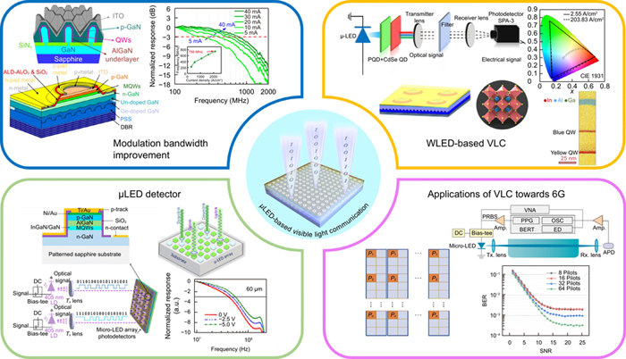
Figure 1.Summary of the review, which includes modulation bandwidth improvement, white light emitting diodes (WLED)-based visible light communication (VLC), micro light emitting diode (μLED) detector and applications of VLC towards 6G.Figure reproduced from: ref.96, 125, 154, 165, American Chemical Society; ref.139, 153, Chinese Laser Press; ref.161, 166, OSA Open Access Publishing Agreement; ref.175, 184, Optical Society of America.
Overview of micro light emitting diode (μLED)-based visible light communication (VLC) systems
Theory of VLC applications
The transmitter in a VLC system uses a visible-light-emitting device, such as an LED or LD, to realize data transmission56, 57. LEDs with diffusers, energy-saving properties, and environmental protection are good light sources for providing uniform illumination. The receiver consists of a photodetector (PD) and signal-processing circuitry. After receiving the optical signal and restoring it to a current signal, the PD generates a voltage signal and completes the digital-to-analog conversion after the signal passes through the signal-processing circuit. The electrical signal is then amplified, equalized, and demodulated to extract valid data.
The channel characteristics in the VLC are distinct from those of the traditional RF system, which is mainly affected by the light source, free-space atmospheric channel, and PD at the receiving end. The modulation bandwidths of the transmitting and receiving ends jointly affect the overall performance of the VLC system. However, in most VLC systems, where the space channel is relatively stable, the devices at the transmitting end mainly affect the communication performance because of the relatively high receiving bandwidth of the PD.
Frequency response is one of the most important parameters required to address when developing LEDs for VLC-system transmitters. For a LED system, the light transfer function is expressed as follows:
where Nin and Nout are the input and output carrier concentrations, respectively. Nout determines the modulated optical power. ω is the angular frequency, and τ is the total response time. The frequency at which the optical modulation power is reduced by half is defined as fc,
where τr and τnr refer to the radiative and nonradiative recombination lifetimes, respectively. τRC is the resistor-capacitor (RC) time constant. As observed in
Eq. (3), the factors affecting the LED modulation characteristics primarily depend on the RC time and carrier radiation lifetime. The junction capacitance affects the RC time and response speed of LED devices, which can delay the signals. The spontaneous emission lifetime of carriers directly affects the time required for carriers from recombination to photons to escape from the device.
Advantages of μLEDs as VLC transmitters
Commercial large-size GaN-based LED dies have an area of a few millimeters per side. However, over such a large area, the response speed is ultimately limited by its RC time constant58. In addition, the carrier recombination process in GaN-based LEDs is affected by the carrier localization effect and quantum confinement stark effect (QCSE), which also leads to an increased carrier lifetime and reduced electro-optical conversion response speed59, 60.
A smaller active area results in reduced geometric capacitance, and consequently a lower RC time constant, which allows μLEDs to have higher modulation bandwidths. Furthermore, μLEDs can withstand higher injection current densities, owing to their uniform current spreading. Tian et al. studied the optoelectronic properties of μLEDs of different sizes, as depicted in Fig. 2(a)61. The current density–voltage (J–V) curves of the LEDs are illustrated in Fig. 2(b). The results indicated that samples of different sizes exhibited strong size-dependent behavior. The smaller μLED has a more uniform current distribution, which leads to a higher injection current density62, 63. They also demonstrated that the current crowding of large-scale samples affects efficiency, especially at high injection densities. The external quantum efficiency (EQE) of the samples was measured. As shown in Fig. 2(c), the smaller μLEDs had lower efficiencies at low current densities, and higher at high current densities. Owing to poor current uniformity, large-sized samples cause a severe efficiency decrease at higher injected carrier concentrations, which results in strong Auger recombination at the edges and other nonradiative recombinations. A higher injection current or efficiency significantly improves the performance of LEDs as VLC emitters.
Figure 2.(a) Schematic of the samples’ structure. (b) J–V characteristics of samples. (c) Current densities of peak EQE, and the efficiency drop of samples. (d) Optical micrograph. (e) Power density and (f) junction temperature of the samples at different current densities. Figure reproduced with permission from: (a–c) ref.61, AIP Publishing; (d–f) ref.64, AIP Publishing.
Zheng et al. investigated the impact of device size scaling on the light output and self-heating of InGaN LEDs64. Figure 2(d) illustrates the optical micrograph of samples with different sizes. The power density versus current density was measured for InGaN LEDs with diameters ranging from 20 to 300 μm (Fig. 2(e)). The study also observed that small-sized samples could withstand higher current densities. The measured junction temperature highlighted in Fig. 2(f) demonstrated that the junction temperature of the smaller samples increased more gradually with the injection current density. They specified 40 μm and 150 μm LED devices for simulation, and the current crowding effect was considered. They discovered significant overheating of the edge of the 150 μm pixel. Thus, the size-dependence effect of the junction temperature can be attributed to the more severe current crowding effect in larger pixels. This explains why smaller samples can withstand higher current densities.
In conclusion, owing to low capacitance and self-heating effect, and good current dispersion, μLEDs possess smaller RC constants and higher injection current densities than conventional wide-area LEDs, resulting in shorter carrier lifetimes and higher modulation bandwidths. Owing to the ultrasmall area, the output optical power can be increased for long-distance and high-speed communication by assembling multiple µLEDs into an array.
Challenges of μLEDs as VLC transmitters
QCSE
Although μLEDs can effectively increase bandwidth compared with traditional LEDs, they still face some challenges in VLC applications. First, commercial μLEDs are typically grown on the (0001) polar c-plane sapphire substrates. This leads to a strong QCSE, which results in reduced efficiency at high injection current densities65. The current GaN-based epitaxy has a hexagonal crystal structure with the highest symmetry compatibility, which results in spontaneous polarization66. Simultaneously, the lattice mismatch between InxGa1−xN and GaN induces strain, which leads to piezoelectric polarization67, 68. The internal spontaneous polarization and piezoelectric polarization tilt the energy-band, and reduce the radiative recombination rate of the carriers, which results in lower modulation bandwidths. In addition to the modulation properties, the QCSE also leads to a wavelength shift and efficiency decrease as the injection current density increases69, 70.
To suppress the QCSE, research has focused on optimizing the epitaxial structure of the device. For example, a thin quantum barrier (QB) can make the carrier distribution more uniform throughout the active region71, 72. Therefore, a thin QB can enhance radiative recombination in the active region and suppress the QCSE with higher bandwidths than those of thick QB. Furthermore, the effect can also be suppressed by growing devices on semipolar or nonpolar substrates.
Carrier localization effect
At low current densities, the QCSE dominates carrier recombination and reduces the radiative recombination rate, which is the main limiting factor for the modulation bandwidth. At high injection condition, the Coulomb shielding effect reduces the polarization caused by the QCSE73, 74. In this case, the carrier localization effect can significantly influence the carrier recombination processes.
The carrier localization effect prevents the nonradiative recombination of carriers inside the quantum well (QW), thereby increasing carrier lifetime59, 75. Hence, for a device with a strong positioning effect, its modulation bandwidth is reduced accordingly. It has been shown that the thickness of the QW affects carrier localization. Zhu et al. fabricated μLEDs with different QW thicknesses and evaluated the extent of carrier localization76. For MQWs with fewer in components, the carrier localization effect was mainly caused by well-width fluctuations77. This suggests that the localization energy can also be evaluated using the variation of the QW band gap. Thus, thicker QW devices with lower MQW bandgap reductions have weaker carrier localization effects, and thus reduced carrier lifetimes.
Size-dependent effect
The reduced size reduces junction temperature and improves current density distribution64, 78, 79. However, as the chip size decreases to the micrometer level, the proportion of the sidewall area increases. The Schockley–Read–Hall (SRH) recombination caused by the sidewall defects in the active region affects the efficiency of the device80. Standard photolithographic techniques introduce severe defects on the surface during dry etching and subsequent processes, which are difficult to avoid during fabrication61. As the chip size decreases, the proportion of the sidewall area increases significantly, and the effect of sidewall defects increases81, 82. More carriers are trapped by sidewall defects during migration, which reduces the efficiency of radiative recombination83. In addition, the SRH recombination is weakened at high injection current densities, which leads to peak EQEs appearing at larger current densities84.
To mitigate the performance degradation, researchers focused on eliminating the sidewall defects of μLED that cause nonradiative recombination. Passivation of sidewalls has been demonstrated as an effective method to reduce the effects of sidewall defects83. In addition, the sidewall defects caused by dry etching can be partially recovered by thermal annealing at high temperatures61.
In addition, as the manufacturing technology of μLED matures, interest in μLED devices with sizes between 1 and 10 μm is increasing. Smith et al. compared the size-dependent EQE of blue and green InGaN μLEDs with sizes as low as 1 μm85. The results show that the EQE of blue μLED evidently decreases for smaller devices. Conversely, green wavelength devices exhibit a smaller size dependence, which is attributed to decreasing surface recombination velocities with increasing In content. Consequently, green μLED sizes smaller than 10 μm have higher EQE than blue devices.
Approaches to increasing the modulation bandwidth
μLED, as an emerging VLC emitter, has rapidly developed in recent years and has made impressive achievements.
Table 1 lists the academic results of VLC systems based on μLED as a light source in recent years, which helped us gain a comprehensive understanding of the recent progress.
| Year | Light source | Modulation bandwidth | Transmission rate | Ref. |
| 2022 | c-plane green μLED (525 nm) | 1.31 GHz | 6 Gbps | ref.86 |
| 2022 | Semipolar blue μLED (447 nm), yellow phosphor | 849 MHz | 2.8 Gbps | ref.87 |
| 2022 | c-plane blue μLED (450 nm) | 880 MHz | 1.1 Gbps | ref.88 |
| 2022 | c-plane red μLED (652 nm) | 271 MHz | 350 Mbps | ref.31 |
| 2022 | Nonpolar blue μLED (463 nm) | 991 MHz | 2 Gbps | ref.89 |
| 2022 | c-plane blue μLED (475 nm) | 1.53 GHz | 5.27 Gbps | ref.90 |
| 2022 | Green quantum dot (QD) LED (495 nm) | 1.22 GHz | 2.1 Gbps | ref.91 |
| 2021 | Semipolar green μLED (550 nm) | 1.1 GHz | 4.3 Gbps | ref.92 |
| 2021 | Green QD-LED (550 nm) | 1.3 GHz | none | ref.93 |
| 2021 | c-plane blue μLED (450 nm) | 251 MHz | 660 Mbps | ref.94 |
| 2021 | c-plane blue μLED (467 nm) | 1.3 GHz | 2 Gbps | ref.95 |
| 2020 | Semipolar green μLED (525 nm) | 775 MHz | 1.5 Gbps | ref.96 |
Table 1. Summary of research progress in the VLC system based on μLED
Currently, blue devices are the most mature among visible LEDs. Thus, blue μLEDs exhibit the highest reported modulation bandwidth among all wavelength devices. Currently, c-plane μLEDs have a lower bandwidth than nonpolar or semipolar μLEDs; however, bandwidths greater than 1 GHz can be achieved by structural optimization or growth of microstructures86, 90, 95, 96. In addition, the use of QDs as active regions also helps reduce the carrier lifetime of the device91, 93. The rest of this chapter describes the methods to increase the modulation bandwidth of the μLED device.
Optimization of C-plane epitaxial structure
InGaN/GaN MQW active regions based on c-plane growth are currently the most mature manufacturing process in the LED industry. Parameter tuning and optimization based on this structure are of great value for the future commercialization of μLED97.
In recent years, structural optimization of c-plane μLED devices has been reported, and the improvement of the modulation bandwidth has mainly focused on enhancing the carrier recombination process. Ferreira et al. fabricated GaN-based μLEDs using Pd as the p-contact metal. Metal contacts with low contact resistances were formed by thermal annealing98. This helped maintain a higher current density. In addition, the face layer was etched on a sapphire substrate, which limited the matching of n-GaN to the active region, thus reducing the capacitance of the device. Rajabi et al. grew blue LEDs with ultrathin InGaN QWs (1 nm) and GaN barriers (3 nm)70. The ultrathin QW device was grown by metalorganic chemical vapor deposition (MOCVD) on a c-plane sapphire substrate. The epitaxial structure included a 1-µm-thick GaN buffer layer, a 2.5-µm-thick Si-doped n-GaN, an MQW active region, a 30-nm-thick electron barrier layer, and a 75-nm-thick p-GaN contact layer. The sample with a thin QW/QB had a faster recombination process than that of a standard sample with a 3 nm/10 nm InGaN/GaN MQW, which was attributed to the higher EH wavefunction overlap in the thin QW. At 2.5-kA/cm2 injection current density, the bandwidth of the thin QW/QB device was 536 MHz. Xu et al. designed and fabricated c-plane blue μLEDs with a thin InGaN layer90. Figure 3(a) shows a transmission electron microscopy (TEM) image of the epitaxial structure of the fabricated LED. The GaN barrier and InGaN well were 1 nm and 12 nm thick, respectively. A 3D schematic of the device is presented in Fig. 3(b), and a cross-sectional scanning electron microscopy (SEM) image of the μLED device is shown in Fig. 3(c). The 60 μm LED pixels were defined using ICP etching processes. Figure 3(d) depicts the modulation bandwidth of the μLED devices. The bandwidth eventually reaches a high value of 1.53 GHz at 6 kA/cm2. Evidently, a 1 nm ultrathin QW structure significantly reduces the QCSE, resulting in a high recombination rate.
Figure 3.(a) Transmission electron microscopy (TEM) image. (b) Three-dimensional schematic and (c) scanning electron microscopy (SEM) image of a µLED. (d) −3 dB bandwidth for different current densities. Schematics of fabrication for the growth of μLEDs on a high-electron-mobility transistor (HEMT) template. (e) Deposition of SiO2. (f) Fabrication of SiO2 microhole arrays. (g) Growth of μLEDs. (h) SiO2 mask removal. (i) Modulation bandwidth and (j) electroluminescence (EL) spectra of device. Figure reproduced with permission from: (a–d) ref.90, IEEE; (e–j) ref.100, under a Creative Commons Attribution (CC-BY) License.
Dry-etching technology can cause inevitable and significant deterioration of μLED performance, and consequently cannot meet the requirements to manufacture high-performance μLEDs29, 99. In addition, with conventional biasing methods, small changes in the forward bias will result in large fluctuations in the injection current density when the LED is operating at a high injection current density, which is difficult to maintain and control. Cai et al. demonstrated the growth of LEDs on predetermined microhole arrays created by SiO2 masks on a high-electron-mobility transistor (HEMT) template100. In this study, direct modulation of the LED emission was achieved by adjusting the 50-nm HEMT gate voltage. The fabrication method is illustrated in Fig. 3(e–h). First, a SiO2 layer was deposited on the AlGaN/GaN template. Subsequently, SiO2 was etched into the microhole arrays. Then, metalorganic vapor-phase epitaxy (MOVPE) was used to reload the patterned HEMT template for further LED growth. The maximum modulation bandwidth reached 1.2 GHz (Fig. 3(i)), which was realized with a 10 V bias in relation to the HEMT and zero gate bias. Figure 3(j) shows the electroluminescence (EL) spectra of a single μLED.
Nonpolar and semipolar plane growth
C-plane LEDs are affected by a strong QCSE, which limits the modulation bandwidth and leads to a decrease in efficiency at high injection current densities66, 68. The deleterious effects of these fields have recently sparked growing interest in nontraditional directions. One approach to overcome the QCSE is to fabricate nonpolar or semipolar structures101. Monavarian et al. measured the modulation bandwidths of μLEDs with different crystal orientations, as shown in Fig. 4(a)65. The bandwidth of the μLEDs grown on nonpolar faces is the highest, followed by those of the semipolar plane and c-plane. The difference in the bandwidth is related to the difference in the wavefunction overlap between the different crystal orientations. Corresponding to the modulation bandwidth, the wavefunction overlap is the highest in nonpolar QWs. When the growth direction of the InGaN/GaN MQW crystal planes is perpendicular to the polar plane, such as (11–20) or (1–100), the polarization field can be completely eliminated102.
Figure 4.(a) Bandwidth for devices with different crystal orientations. (b) Schematic and (c) frequency response of the nonpolar μLED. (d) Schematic diagram of semipolar (20–21) green μLED structures. (e) Time-resolved photoluminescence (TRPL) curves of semipolar μLED and c-plane μLED. (f) Frequency response of the semipolar μLED. (g) PR and (h) frequency responses of μLED array. (i) BER and signal-to-noise ratio at 4.5 Gbit/s transmission rate with different sampling rates. Figure reproduced with permission from: (a) ref.65, AIP Publishing; (b, c) ref.103, IEEE; (d–f) ref.96, American Chemical Society; (g–i) ref.109, Optica Publishing Group.
Rashidi et al. demonstrated a nonpolar m-plane blue μLED for high-speed VLC103. As depicted in Fig. 4(b), the device is grown on a freestanding GaN substrate formed by metal–organic chemical vapor deposition on a nonpolar (10–10) face. The normalized frequency responses of the nonpolar μLEDs at different current densities are shown in Fig. 4(c). With an injection current density of 1000 A/cm2, the maximum –3 dB bandwidth of the LEDs reached a maximum of 1.485 GHz.
Although devices grown on nonpolar planes can effectively eliminate polarization fields, achieving long-wavelength emissions >510 nm with such nonpolar a-plane or m-plane LEDs remains challenging. Additionally, nonpolar LEDs have a low EQE, owing to low In incorporation. The semipolar plane is also a fundamental solution to the QCSE, which makes semipolar μLEDs a strong contender for high-bandwidth devices. The chemical potential for incorporating In atoms into semipolar planes is considerably lower than that into nonpolar planes, owing to the lower repulsive interactions between the semipolar GaN surface and the In atoms. This facilitates the growth of long-wavelength InGaN/GaN devices 104. Chen et al. realized 540-nm green μLEDs with a high –3 dB bandwidth using semipolar (20–21) GaN epitaxy96. Figure 4(d) demonstrates the optimized μ-LED device structure. The Al2O3 layer deposited by atomic-layer deposition (ALD) reduced the effect of sidewall defects. The carrier lifetime τ of the semipolar μLED measured by time-resolved photoluminescence (TRPL) is 2.65 ns, as shown in Fig. 4(e), which is much lower than that of the c-plane μLED used as a reference. The shorter lifetime of the semipolar samples is owing to the weak polarization field. This results in a larger electron-hole wavefunction overlap, which reduces τr105-107. A shorter carrier recombination corresponds to faster carrier transport; thus, green semipolar μLEDs can achieve –3 dB bandwidths up to 756 MHz, as shown in Fig. 4(f).
The fast response time and small size of semipolar μLEDs enable a high output power, high modulation bandwidth, and high efficiency when integrated into arrays108. Lin et al. designed a 2×2 semipolar green μLED array with a size of 50 µm109. Semipolar (20–21) oriented GaN layers were synthesized on a patterned sapphire substrate. All the elements in the μLED array were connected in parallel. The device was fabricated by employing nanostructured grating patterns, which improved the polarization ratio (PR)110. Figure 4(g) reveals that the output degree of polarization (DOP) of the semipolar μLED increased by 0.71 to favor liquid-crystal display applications. With an injected current of 23 mA, the −3 dB bandwidth of the μLED array was 800 MHz, as shown in Fig. 4(h). A transmission rate of 4.5 Gbps can be achieved using 8-QAM OFDM modulation, as shown in Fig. 4(i).
InGaN QDs in active region
GaN-based QDs have received significant research attention, owing to their strong quantum-confinement capabilities111-114. Unlike QWs, which only bear compressive stress from the direction parallel to the interface, the compressive stresses on QDs in three dimensions cancel each other; thus, the strain is smaller than that of QWs. In addition, QDs exhibit a stress-releasing mechanism during epitaxy115. Incidentally, the use of QDs instead of QWs can reduce the volume of the active region, which is beneficial for accelerating the carrier recombination process and increasing the device modulation bandwidth.
Based on the potential of GaN-based QDs devices in VLC applications, Wang et al. grew self-assembled QDs in the Volmer-Weber mode93. This resulted in QDs without a wetting layer (WL), owing to a sufficiently large lattice mismatch. The WL in the QD decreases the carrier localization, thereby limiting the recombination and increasing the carrier lifetime112. Thus, the bandwidth of the μLED device reaches 1.3 GHz at a relatively low current density of 509 A/cm2.
QCSE suppression was also observed in QD-based long-wavelength LEDs, with a blue-shift level similar to those of nonpolar or semipolar plane devices with increasing injection current116, 117. Wan et al. demonstrated a phosphor-free single-chip WLED using a InGaN QDs structure118. Figure 5(a) shows a schematic of the epitaxial structure. A HRTEM image of the MQW region is shown in Fig. 5(b), where alternately stacked light and dark layers represent GaN QBs and InGaN QWs, respectively. The modulation bandwidth of the WLED at different current densities is summarized in Fig. 5(c). The bandwidth of a traditional WLED (a few MHz) is much lower than that of the fabricated WLED. One reasonable explanation is that the QCSE of InGaN/GaN QDs is smaller than that of the InGaN/GaN QWs. The –3 dB bandwidth reached a maximum of 150 MHz. Eye diagrams for transmission rates of 50 and 127 Mbps are shown in Fig. 5(d). Wei et al. designed a green μLED with five-layer InGaN QDs91. Figure 5(e) shows a TEM image of the 5-layer InGaN QD structure as the active region. The heights of QDs are distributed over approximately 2–3 nm, and the horizontal distribution is denser, which helps shorten the carrier recombination lifetime. Figure 5(f) shows the extracted –3 dB bandwidth. The bandwidth of QD green μLEDs with 50 and 75 μm active region diameters can reach 1.22 and 1.14 GHz, respectively. As shown in Fig. 5(g), the 75 μm sample can achieve a maximum transmission rate of 2.0 Gbps.
Figure 5.(a) Schematic. (b) HRTEM image of the QWs. (c) Bandwidth of single chip WLED vs. injection current density. (d) Eye diagram at transmission rate of 50 and 127 Mbps. (e) TEM images of InGaN QDs. (f) –3 dB bandwidth and (g) BER at different current densities. Figure reproduced with permission from: (a–d) ref.118, Optica Publishing Group; (e–g) ref.91, ACS Publishing.
Microstructure
Exploiting nanostructures in the active region to excite resonant interaction between QWs and QDs in QD-LEDs is another approach to fabricate high-modulation bandwidth devices. Nonradiative resonance energy transfer (NRET) between QWs and QDs has been demonstrated to use exciton-exciton coupling to accelerate the recombination rate119-121. Wan et al. fabricated quantum-well-QD-SP coupled LEDs in nanopore LED (H-LED) structures filled with QD and silver nanoparticles, which had a shorter carrier lifetime compared to H-LED and QD-only filled samples (QD-LEDs)122. In QD-LEDs, excitons close to the nanohole sidewall can undergo NRET. This process can significantly increase the decay rate of excitons in QWs and lead to shorter carrier lifetimes. Owing to the NRET, the recombination of excitons in the QWs of quantum-well-QD-SP coupled LEDs is faster than that of QD-LEDs, which further decreases the fast carrier lifetimes.
Similar to QDs, InGaN nanowires are another low-dimensional structure. Unlike planar μLEDs, nanowire μLEDs have independent nanowires within each pixel. Thus, the surface-to-volume ratio remains constant for different pixel sizes123, 124. This enables a higher efficiency in nanowire μLEDs. Nanowire-based LEDs can also be considered in VLC applications. Nami et al. grew GaN nanowires on c-plane sapphire substrates using MOCVD125. InGaN/GaN QW/barriers were grown around the core-shell nanowires and 60 μm nanowire μLEDs were fabricated. SEM images of the nanowires after QW and p-GaN growth and the fully fabricated nanowire μLED device are shown in Fig. 6(a–c), respectively. The nanowires contained nonpolar m-plane sidewalls. The bandwidth of the nanowire μLED was 1.19 GHz, as shown in Fig. 6(d). The high modulation bandwidth of nanowire μLEDs is the result of electron-hole wavefunction overlap in nonpolar QWs, which increases the rate of recombination processes.
Figure 6.SEM images of the nanowires after (a) QW and (b) p-GaN growth and (c) the fully fabricated nanowire μLED device. (d) −3 dB bandwidth of device. (e) TRPL of PLED and control LED. Figure reproduced with permission from: (a–d) ref.125, American Chemical Society; (e) ref.129, American Chemical Society.
Recently, plasmonic devices have received extensive attention in the field of VLC for surface plasmons, which can create energy transition channels for electron-hole pairs in devices via QW-SP coupling122. Possible resonant coupling conditions between QWs and bulk silver have been reported126; therefore, the plasmonic coupling is extensively used in GaN-based LEDs127, 128. Ferrari et al. fabricated a nanostructured plasmonic light-emitting diode (PLED)129. Nanoholes were patterned into the MQW region through the p-GaN layer and then coated with a thin Ag film. This scheme exploits the nanostructural properties of silver films to couple SPP to the far field. The decay curves of the PLED versus the control LED are shown in Fig. 6(e). The lifetimes of PLED and control LED are 0.08 ns and 3 ns, respectively, which is equivalent to a shortening by a factor of several dozen. This paves the way for the fabrication of high-speed ion-enhanced μLEDs used for VLC.
μLED-based WLED VLC system
VLC technology enables LED-based lighting infrastructure to offer both lighting and data communication. According to statistics, lighting electricity accounts for approximately 20% of the global electricity consumption, which urgently requires the development of efficient and environmentally friendly lighting sources. Therefore, compared with monochromatic blue or green LEDs, WLEDs that can provide lighting functions while offering a high luminous efficiency, long service life, and environmental protection characteristics have greater application prospects in VLC. In recent years, VLC systems utilizing WLEDs have been demonstrated130-132.
PL WLEDs
WLEDs based on μLEDs are attractive, owing to the characteristics of a high modulation speed, high efficiency, and long lifetime. The ideal white μLED is a monolithic integration of three separate μLED chips containing red, green, and blue (RGB) emissions. Research on high-efficiency blue μLEDs is relatively mature. However, the “green gap” limits the performance of the green µLED133. Green μLEDs have a high proportion of indium, which requires a relatively low temperature when fabricating, which leads to strong QCSEs and a reduced radiative recombination efficiency. In addition, red µLEDs are mainly fabricated using the AlGaInP material system, which leads to long carrier diffusion length and enhanced non radiation recombination134, 135. Therefore, the efficiency degradation of red µLEDs is more severe with the size of devices decreasing to a few microns. Another problem with implementing RGB µLEDs is that the working voltage between different pixels is different, which complicates driver circuit design. For photoluminescent WLEDs, trichromatic components are typically derived from emissive materials pumped by blue or UV chips.
WLEDs based on phosphor film for VLC
Phosphor-based WLEDs based on blue LEDs exciting yellow phosphor are among the most common lighting devices. However, the modulation bandwidth of WLEDs is significantly limited by the long response time of LEDs and fluorescent materials. This leads to difficulties in realizing high-speed VLC with the electro-optic (EO) bandwidth of conventional WLEDs of only a few MHz. Therefore, previous studies have proposed several methods to increase speed, including the addition of equalization circuits or higher-order modulation methods. Minh et al. increased the bandwidth of a WLED to 50 MHz using an analog equalizer and achieved a transmission rate of 100 Mbps136. Hsu et al. proposed the use of adaptive Volterra filtering for phosphor-based WLED VLC systems, and a transmission rate of 700.68 Mbit/s was achieved137. Hsu et al. demonstrated a 3 × 3 multiple-input multiple-output (MIMO) WLED VLC system with a data rate of 1 Gbps using a pre-equalizer circuit and OFDM modulation138.
To address the low modulation bandwidth of WLEDs fabricated based on phosphor films, blue μLEDs can be integrated with color-conversion materials. Chun et al. achieved high-speed transmission of 1.68 Gbps using a blue μLED combined with phosphor films139. Huang et al. proposed a white-light system based on blue μLED arrays with phosphor color conversion to achieve a 127.3 MHz EO bandwidth140. Semipolar μLEDs also provide unique advantages in WLED systems, owing to their excellent performance. Zhang et al. utilized semipolar (20–21) blue μLEDs to pump yellow phosphors to realize a high-speed VLC system87. A phosphor film was coated onto the surface mounted devices (SMD) package to generate white light, as shown in Fig. 7(a). Figure 7(b) shows a photograph of the fabricated WLED device. The optoelectronic and communication properties of these devices were also evaluated. The spectrum of the blue μLED array with yellow phosphor is displayed in Fig. 7(c), with peak wavelengths of 447 and 545 nm. The normalized frequency response of the μLED array was measured, as shown in Fig. 7(d). The bandwidth of the semipolar blue μLED, yellow component and the overall white-light VLC system are 1042.5, 24, and 849 MHz, respectively. Figure 7(e) shows the BERs curves of the white-light VLC system. A data rate of 2.805 Gbps can be achieved using OFDM modulation; thus, this phosphor-based white μLED device can be applied to high-speed VLC.
Figure 7.(a) Schematic diagram of WLED device based on semipolar μLED array. (b) Photographs of the μLED array without current. (c) Spectrum of the WLED. (d) Measured normalized frequency response of μLED array. (e) BER curve of the white-light VLC system. Figure reproduced with permission from: (a–e) ref.87, under the Optica Open Access Publishing Agreement.
WLEDs based on QDs color conversion for VLC
Despite the excellent performance of phosphor-based WLEDs, their modulation bandwidth is significantly limited by the color-conversion materials. The radiative relaxation of phosphors is related to the trap energy state with a certain depth, which causes the afterglow lasting a few microseconds37, 141-143. Therefore, the development of color-conversion materials with a fast response speed is crucial for VLC applications. QDs are nanoscale semiconductor crystals that can modulate the emission wavelength by changing sizes144-146. Compared to traditional fluorophores, QDs have a wide range of absorption spectra, including blue and UV bands147, 148. More importantly, for VLC applications, QDs typically have short fluorescence lifetimes in the order of nanoseconds. Therefore, QD-based color-conversion layers can achieve high modulation bandwidths and high data rates. Ruan et al. demonstrated that AgInS2/ZnS core/shell QDs are good color-conversion materials for WLEDs and can conduct VLC149. Xiao et al. increased the modulation bandwidth of QD-WLED by 67.75% using CdSe/ZnS QDs130. Cao et al. used GHz high-bandwidth blue LED devices combined with CdSe/ZnS QDs to achieve white light emission with an overall modulation bandwidth of 637.6 MHz for visible light communication150.
Halide perovskite quantum dots (PQDs) exhibited narrow emission and short fluorescence lifetimes and have garnered broadening research interest for VLC151. Shi et al. combined blue GaN-based μLEDs with CsPbBr1.8I1.2 yellow PQDs for color conversion to fabricate a white-light VLC system, as illustrated in Fig. 8(a)152. Modulation bandwidths of 73 MHz and 85 MHz were achieved for PQDs and overall VLC system, respectively. Wu et al. proposed a PNC-μLED device based on a semipolar (20–21) blue μLED array, mixing green CsPbBr3 and red CsPbBrI2 PNCs powders as the color conversion layer139. The PNCs were encapsulated in a SiO2 shell using high-temperature sintering, which significantly improved the stability. Figure 8(b) illustrates the PL intensity of PNCs after blue radiation aging. The SiO2-embedded samples exhibited remarkable stability and no degradation under blue irradiation. The bandwidth of PNCs is typically in the order of tens of MHz, and a filter was used to remove the red and green light generated by PNCs in the experiment. The blue light passing through the filter was coupled to a photodetector, and the highest bandwidth of the PNC-μLED was measured as 655 MHz at a current of 200 mA (Fig. 8(c)).
Figure 8.(a) White-light VLC system consisting of perovskite quantum dot (PQD) and blue μLED. (b) The longevity of the PL properties of the PNCs. (c) Frequency response of the PNC-μLED. (d) TRPL measurement for semipolar μLED, PQD and CdSe QD papers. (e) Frequency response of PQD paper and PQD film. (f) TEM images of RQDs. (g) TRPL measurement for YQDs and RQDs. (h) Frequency response of red and yellow PNC-PMMA. Figure reproduced with permission from: (a) ref.152, American Chemical Society; (b, c) ref.139, American Chemical Society; (d, e) ref.153, Optica Publishing Group; (f–h) ref.154, American Chemical Society.
Currently, the in-depth study of PQDs is committed to fabricating color-conversion layers with higher modulation speeds, which will further increase the transmission rate. Singh et al. proposed a flexible white-light VLC system consisting of nanostructured green CsPbBr3 PQD paper, red CdSe QD paper, and semipolar blue μLEDs153. CsPbBr3 PQD paper was prepared by mixing a QD solution with a cellulose nanocrystal suspension. The PQD paper fabricated using this method has a nanostructure that provides a strong quantum confinement effect to increase the recombination rate. The TRPL measurements of PQD and CdSe QD are shown in Fig. 8(d), and the calculated average lifetimes are calculated as 5.92 and 12.88 ns, respectively. The shorter carrier lifetime of the PQD paper is attributable to the quantum confinement effect. The PQD paper exhibits a higher bandwidth of 229 MHz compared to the 111 MHz of the PQD film embedded in the polymer fabrication, as shown in Fig. 8(e), which is suitable for achieving a high-speed VLC. Wang et al. proposed a white-light VLC system using red/yellow-emitting CsPb(Br/I)3 and CsPbI3 PNC-PMMA films combined with blue μLEDs154. Figure 8(f) shows the TEM images of RQDs with an average size of 5.73 ± 0.95 nm. The carrier lifetimes of yellow PNC-PMMA and red PNC-PMMA are 11.2 and 3.5 ns, respectively, as shown in Fig. 8(g). Such short lifetimes indicate a higher modulation bandwidth. This was primarily attributed to the small average size of the red QDs, which led to significantly accelerated carrier relaxation rates. The normalized frequency response of the PNC film was further tested (Fig. 8(h)). The –3 dB bandwidths of red and yellow PNC-PMMA were 822 and 347 MHz, respectively, which exhibited good potential for indoor high-speed white-light communication systems.
Notably, PQDs contain toxic elements, such as Pb and Cd, which cause pollution and limit the wide application of QDs. The fabrication of QDs without toxic elements has become a subject of intense interest recently. Soheyli et al. reported a novel aqueous-phase approach for the preparation of multicomponent In-based QDs155. The absorption and photoluminescence emission spectra of the as-prepared QDs were optimized by altering their composition to obtain Zn-Ag-In -S/ZnS and Cu-Ag-In-S/ZnS QDs. In addition to displays, such QDs are equally promising for VLC applications.
Electroluminescent WLEDs
Although WLEDs based on color-conversion layers have made significant progress and possess a relatively high luminous efficiency, we emphasize that such a WLED involves energy loss during the down-conversion process. The current efficiency (defined as the ratio of luminance to current) of color-conversion-based WLEDs is lower than that of electroluminescent multicolor QW WLEDs. Therefore, electroluminescent WLEDs without color-conversion layers or phosphors are attractive because they can overcome the drawbacks of phosphor-converted WLEDs, such as Stokes energy conversion loss, and they have good stability156, 157.
Blue and yellow QWs are typically grown on GaN substrates to produce monolithic WLED devices. During fabrication, the device structure is optimized to realize WLED devices more suitable for VLC. Semipolar GaN materials have high polarization ratios, a large wavefunction overlap, and short carrier lifetimes, which make monolithic white semipolar GaN μLEDs more attractive. Khoury et al. grew high-efficiency monolithic white semipolar (20–21) LEDs on 4-inch sapphire templates158. An overall PR of 0.3 was achieved based on the blue and yellow QWs. The μLEDs in their work achieved high modulation bandwidths of up to 660 MHz. They also reported that the PR increased in devices with longer wavelengths at higher compositions, which suggests that monolithic white semipolar LEDs have potential applications as LCD backlights159, 160.
In another study, Li et al. fabricated white semipolar (20–21) μLEDs by adopting a top blue QW and bottom yellow QW directly grown on a (20–21) semipolar bulk GaN substrate161. The QWs comprised a 3 nm In0.28Ga0.72N yellow QW and a 3 nm In0.13Ga0.87N blue QW. Figure 9(a) shows the reconstruction side view of the blue and yellow QW and EBL layers. Blue and yellow QWs with different In compositions are clearly observed. Figure 9(b) illustrates the distribution analysis of the In components in blue and yellow QWs. Subsequently, the communication performance of the µLED device was tested. Figure 9(c) indicates the modulation bandwidth for semipolar white µLEDs of all sizes. Devices with sizes of 20 and 40 µm achieved high modulation bandwidths of up to 410 MHz. Haggar et al. fabricated green, yellow, and amber semipolar LEDs on semipolar (11–22) GaN on m-plane sapphire substrates162. InGaN SQWs with different In components were used to achieve long-wavelength emissions of different colors. Because all the samples were fabricated using the same material system, a white-light monolithic LED chip can be integrated. The performance of the samples as VLC transmitters was measured. Figure 9(d) shows the received power spectrum of the adaptively loaded OFDM waveform, with maximum data rates of 4.42 Gbps, 3.72 Gbps, and 336 Mbps for the green, yellow, and amber devices, respectively. Figure 9(e) shows the corresponding constellation diagram.
Figure 9.(a) Composition of WLED active region. (b) The distribution analysis of In components in QWs. (c) Modulation bandwidths of different sizes µLEDs. (d) Power spectra of OFDM-modulated waveforms measured at data rates of 4.42 Gbps, 3.72 Gbps, and 336 Mbps. (e) Constellations under corresponding order QAM modulation. Figure reproduced with permission from: (a–c) ref.161, under the OSA Open Access Publishing Agreement; (d, e) ref.162, under a Creative Commons Attribution (CC-BY) License.
VLC based on μLED detector
As discussed in the previous section, μLEDs with unique properties have been widely used as the transmitter in VLC. However, relatively few studies have used μLEDs as light receivers. Owing to their sensitivity to light, LEDs can potentially be used as PDs. Most commercial PDs are based on Si or GaAs, and the receiving spectrum covers a wide range, which causes significant optical noise. In addition to the advantages of low dark current and high sensitivity, GaN-based LEDs offer wavelength selectivity when used as PDs and can only receive light waves lower than their own wavelengths; that is, they have natural filtering properties43, 163, 164. This topic has attracted significant academic interest. There is no need to change the MQW structure or the material of the μLEDs used as PDs. Based on the photoelectric effect, photogenerated electron–hole pairs can realize optoelectronic (OE) conversion when the MQW is excited by the input optical signal. Although the responsivities of μLED-based detectors are generally lower than those of Si or GaAs receivers, they are comparable. Owing to the wavelength selectivity of LED detectors, a higher sensitivity can be achieved for a certain band than current commercial Si or GaAs receivers165. In addition to the advantages of LED-based PDs, μLED-based PDs show great potential for realizing high-speed MIMO VLC for light detection. Owing to the small size and easy integration of μLEDs, μLEDs array-based PDs can enable multi-user communication and increased data rates, compared with individual μPDs. Thus, μLED displays can be used as both transmitters and detectors to achieve duplex high-speed VLC.
As part of the µLED array for VLC detectors, Liu et al. proposed a blue μLED array for use as a PD in VLC165. That study realized a μLED PD-based 2 × 2 MIMO VLC (Fig. 10(a)). Two LDs were used as transmitters, and a μLED array was used as the detector. Figure 10(b) illustrates the I–V characteristics of the μLED PD measured in the dark and under illumination. As observed in the figure, the current of the μLED PD gradually increases with the increase in the received power, owing to the photogenerated carriers. Additionally, for μLED-based PDs, at zero bias, high photosensitivity was observed owing to the low dark current. Figure 10(c) shows the measured responsivity of the μLED PD for different wavelength bands. The figure reveals that the μLED PD does not respond to wavelength bands above 450 nm, reflecting outstanding wavelength selectivity. The frequency response characteristics of μLED PDs under 405-nm LD illumination are illustrated in Fig. 10(d). Bandwidths up to 41.2 MHz can still be achieved at 0-V bias. Figure 10(e) shows an eye diagram captured by the μLED PD at a transmission rate of 160 Mbps and a bias of –5 V. The obtained results demonstrate the ability of μLED PDs to detect fast optical signals for high-speed communications.
Figure 10.(a) Cross-section of the μLED and schematic setup for VLC system using the μLED based photodetectors. (b) Current–voltage (I–V) curves of the μLED-based PD with diameters of 60 μm under darkness and illumination. (c) Responsivities of the μLED-based PD measured for various laser wavelengths. (d) Frequency response for μLED-based PD. (e) Eye diagrams at a transmission rate of 160 Mbps. (f) Cross-section of semipolar green μLEDs. (g) Frequency responses of μLED PD. (h) BERs with μLEDs as PD at a transmission rate of 540 Mbps. Figure reproduced with permission from: (a–e) ref.165, American Chemical Society; (f–h) ref.166, under the OSA Open Access Publishing Agreement.
In the previous discussion, we stated that semipolar μLEDs had a high application potential as VLC transmitters, owing to their higher response speed. However, semipolar μLEDs can also achieve high-speed signal detection, owing to their shortened carrier lifetime. Chang et al. investigated the performance of green semipolar (20–21) μLEDs as VLC photoreceivers166. The cross-section of the semipolar μLED array used as a PD with a diameter of 30 μm is illustrated in Fig. 10(f). Devices grown in the semipolar direction can provide higher modulation responses, owing to the larger overlap of electron-hole wave functions and shortened carrier lifetime. A VLC system was built with the semipolar μLED as the receiver. The OE responses of the semipolar μLED PD were measured under different biases, as shown in Fig. 10(g). At a bias of 5 V, the measured 3 dB OE bandwidths are 228 MHz, which are considerably larger than those of the LED PDs and other μLED PDs. Figure 10(h) shows the experimental BER curves obtained using the μLED PD array at a data rate of 540 Mbps. This indicates that semipolar μLEDs have a high application value as PDs in high-speed VLC systems.
Novel applications of VLC towards 6G
The development of next-generation cellular networks has aimed at faster and more reliable solutions with expansive and more complex feature sets. Networks for 6G will have higher transmission speed requirements167, 168. Studies on epitaxial design, crystal orientation, and microstructure have enabled the fabrication of μLEDs with high-speed modulation characteristics that have demonstrated Gbps-level data throughput. This will promote the development of μLED-based VLC systems as a key wireless technology for 6G. In addition, the use of high-frequency waves raises user concerns about the potential hazards of radio frequencies to humans in these frequency bands. From this perspective, the VLC system will provide users with the option of using an RF-free connection169. Adding this optical-transport interface gives device manufacturers a competitive advantage. Therefore, optical wireless communications must create a viable concept that complements RF communications as part of 6G.
Underwater VLC technology
Global extensive access is an important aspect in the development of 6G. However, underwater communication, such as in the oceans, performance has always been unsatisfactory. Underwater communication technology is important for realizing the integration of a 6G network. The realization of functions, such as wireless fusion networking and noncontact interaction, between different devices in the oceans requires underwater communication support.
Acoustic waves are the most used method of underwater communication; however, they have a low carrier frequency, which leads to a limited bandwidth170. Although RF waves have a higher transmission bandwidth than sound waves, owing to the skin effect, the transmission distance is directly limited, making it difficult to implement the main task of 6G underwater communication171, 172. Wavelengths between 450 and 550 nm have considerably less attenuation than other light bands, which indicates that blue–green light is of great significance in underwater communication and lays the foundation for underwater visible-light communication (UVLC). Compared with other wireless communication methods, UVLC has the advantages of high transmission rate, strong anti-interference ability, and high security173. μLEDs have exhibited great potential for medium/short-distance high-speed underwater transmission through a high modulation bandwidth174.
Recently, Wei et al. fabricated a QD blue μLED with a size of 75 μm for UVLC175. The growth-interruption method was employed to fabricate QD active region. Figure 11(a) and 11(b) illustrate a schematic and a photograph of the experimental setup of the μLED-based UVLC system, respectively, over a 3 m communication distance. At a current density of 582.54 A/cm2, the modulation bandwidth of the UVLC system increased to 1.03 GHz (Fig. 11(c)). Thus, a transmission rate of 2 Gbps could be achieved with a BER of 2.03 × 10⁻³. Kim et al. proposed a 32 × 32 high-power MQW flip-chip blue μLED array (μLED-on-HEMT) integrated into AlGaN/GaN-based HFETs for UVLC176. The uniform optoelectronic properties were obtained for each pixel of the integrated μLED-on-HEMT array. The light output power (LOP) and current of the μLED-on-HEMT device were measured as functions of VDD (Fig. 11(d)). The LOP was 3.7 mW, and VDD was 10 V. Each pixel of the integrated array of μLEDs exhibited a high LOP of modulation at 450 nm, which demonstrated the potential for use in UVLC. Lin et al. also demonstrated that, in addition to serving as transmitters, μLEDs could realize optical detection and underwater charging in duplex UVLC94. At 0 V bias, the maximum transmission rate of the μLED PD-based UVLC system was 52.5 Mbps. Under a high received optical power, the device could efficiently collect photogenerated carriers. Through circuit design, the μLED can simultaneously collect DC energy that is irrelevant to the transmission information for charging, while realizing high-speed AC signal detection, which is sufficient to drive a 660 nm LD.
Figure 11.(a) Schematic of setup and (b) photograph and (c) frequency responses of the μLED-based UOWC system. (d) Light output power (LOP) and forward current characteristics of the μLED-on-HEMT arrays. Figure reproduced with permission from: (a–c) ref.175, under a Creative Commons Attribution license; (d) ref.176, under a Creative Commons Attribution License.
Visible light communication based on AI discipline
VLC applied to 6G must span multiple scenarios, which will lead to complex and changeable channels. Therefore, signals will be affected by nonlinear distortions during transmission. In addition to the complexity of the channel, the nonlinear response of the transmitter LED and PD may also complicate the model of the VLC system, making fitting it with traditional equalization algorithms difficult.
Recently, AI has been widely used in VLC for tasks such as higher-order modulation and demodulation, channel estimation, indoor positioning, and nonlinear equalization. Nonlinearities in high-speed VLC systems can be mitigated by employing clustering schemes and neural networks (NNs). For the application of the clustering, Lu et al. proposed the use of the K-means algorithm to cluster constellation points with a center shift under nonlinear conditions to obtain a new distribution center of constellation points under the condition of deformation177. Wen et al. proposed a novel sampling frequency offset mitigation scheme178. The algorithm was based on K-means clustering, which enabled the accurate clustering of constellation points with phase offsets. Simultaneously, with the development of GPUs and advancements in digital signal-processing technology, equalizers based on deep NNs (DNNs) are becoming popular. Chi et al. proposed a high-speed kernel-function-based DNN for nonlinear mitigation179. Additionally, Chen et al. proposed a hybrid frequency-domain-assisted temporal convolutional NN to compensate for the nonlinear distortions in UVLC systems180.
To meet the requirements of ever-increasing data in the 6G era, various efforts must be made to increase the data rate to the order of 10 Gbps. From a device perspective, combining an NN-based equalizer with μLEDs with a high EO bandwidth is a feasible solution to maximize the transmitted data. In addition to DNNs, the potential of an artificial NN (ANN) program for high-speed communication owing to its approximation to arbitrary functions was demonstrated181-183. Wei et al. combined high-bandwidth μLED and ANN equalizers in a VLC system to achieve higher data rates. The ANN consists of five layers184. The training dataset was obtained from the Winner channel model dataset. The system structure is illustrated in Fig. 12(a), and a schematic of the arrangement of pilots in the OFDM symbols is shown in Fig. 12(b). The BER simulation results using blocks with pilot lengths of 8, 16, 32, and 64 were measured, as shown in Fig. 12(c). The ANN equalizer achieved relatively good results in the low signal-to-noise (SNR) range. For a specific number of pilots, the BER decreased rapidly and then settled into a higher SNR range. Based on this system, the data rate vs. BER, with two μLEDs as transmitters, was tested (Fig. 12(d) and 12(e)). The 75 µm μLED exhibited better performance and could transmit data at a rate of 8.75 Gbps.
Figure 12.(a) Schematic of the VLC system based on μLED and ANN equalizers. (b) Schematic of the arrangement of pilots. (c) BER in simulation with different pilot lengths. BER performance for (d) 50- and (e) 75-µm blue μLEDs. Figure reproduced with permission from ref.184, Optical Society of America.
Conclusions
As the research on μLED devices expands, the μLED-based high-speed VLC is garnering increasing interest. This review summarizes the advantages and challenges of μLEDs in VLC systems. Methods to improve the modulation bandwidth of μLEDs were introduced. In addition to conventional c-polar epitaxial structure optimization and semi/nonpolar GaN epitaxial growth, μLEDs using microstructures or InGaN QDs as active regions can also improve the radiative recombination rate. μLEDs are considered bright solid-state lighting sources compared with different classes of WLEDs for VLC. Similarly, μLEDs can also be used as detectors in VLC systems. Finally, the prospects of VLC in 6G and the latest high-speed VLC applications were introduced. Given the high-speed transmission advantages, μLED-based VLC is expected to become an ancillary technology for 6G and cooperate with other communication technology to benefit our daily lives.
Acknowledgements
We appreciate Prof. Rong Zhang and Prof. Minghui Hong from Xiamen University for the helpful discussion. We are grateful for the financial support from the National Natural Science Foundation of China (62274138, 11904302), Science and Technology Plan Project in Fujian Province of China (2021H0011), Fujian Province Central Guidance Local Science and Technology Development Fund Project in 2022 (2022L3058), Major Science and Technology Project of Xiamen, China (3502Z20191015) , and Foshan Hi-tech Zone High-tech Industrialization Entrepreneurial Team Special Guidance Fund in 2022 (222019000131).
The authors declare no competing financial interests.
References
[22] Parikh H, Chokshi J, Gala N, Biradar T. Wirelessly transmitting a grayscale image using visible light. In Proceedings of 2013InternationalConferenceonAdvancesinTechnologyandEngineering (ICATE) 1–6 (IEEE, 2013);http://doi.org/10.1109/ICAdTE.2013.6524748
[28] O'Brien DC. Visible light communications: challenges and potential. In Proceedings of the IEEE Photonic Society 24th Annual Meeting 365–366 (IEEE, 2011);http://doi.org/10.1109/PHO.2011.6110579.
[50] Katz M, Ahmed I. Opportunities and challenges for visible light communications in 6G. In Proceedings of the 2nd6GWirelessSummit (6GSUMMIT) 1–5 (IEEE, 2020);http://doi.org/10.1109/6GSUMMIT49458.2020.9083805.
[134] Bulashevich KA, Karpov SY. Impact of surface recombination on efficiency of III-nitride light-emitting diodes. Phys Status Solidi (RRL)-Rapid Res Lett10, 480–484 (2016).
[163] Chun H, Rajbhandari S, Faulkner G, Tsonev D, Haas H et al. Demonstration of a Bi-directional visible light communication with an overall sum-rate of 110 Mb/s using LEDs as Emitter and Detector. In Proceedings of 2014IEEEPhotonicsConference 132–133 (IEEE, 2014);http://doi.org/10.1109/IPCon.2014.6995247