In this work, a GaN p-i-n diode based on Mg ion implantation for visible-blind UV detection is demonstrated. With an optimized implantation and annealing process, a p-GaN layer and corresponding GaN p-i-n photodiode are achieved via Mg implantation. As revealed in the UV detection characterizations, these diodes exhibit a sharp wavelength cutoff at 365 nm, high UV/visible rejection ratio of , and high photoresponsivity of 0.35 A/W, and are proved to be comparable with commercially available GaN p-n photodiodes. Additionally, a localized states-related gain mechanism is systematically investigated, and a relevant physics model of electric-field-assisted photocarrier hopping is proposed. The demonstrated Mg ion-implantation-based approach is believed to be an applicable and CMOS-process-compatible technology for GaN-based p-i-n photodiodes.
1. INTRODUCTION
Ultraviolet (UV) photodetectors (PDs) have drawn extensive attention owing to their important civilian and military applications, including chemical/biological sensing, flame warning, missile plume detection, and solar astronomy [1–7]. Advantageous optical and electrical properties of GaN, together with a room-temperature (RT) bandgap of 3.41 eV (365 nm) make it highly promising for visible-blind UV detections [1–4]. The GaN p-i-n diode is one of the most fundamental UV PD structures, with advantages including high speed, sharp UV/visible cutoff ratio, low dark current, and capability of operating in photovoltaic mode [1–3]. In most of the prior GaN p-i-n photodiodes, the p-GaN region was fabricated with an in situ process in a metal organic chemical vapor deposition (MOCVD) system [1–4]. Comparatively, ion implantation is another potential approach for p-GaN layer doping, possessing advantages in compatibility with complementary metal oxide semiconductor (CMOS) technology, higher uniformity, and higher yield. Therefore, an ion-implantation-based GaN p-i-n diode could become fairly competitive for future mass production if it could be realized for UV detection. However, serious implantation-induced damage and low activation rate make it quite challenging to realize p-type doping via ion implantation in GaN [8–11]. Resultantly, the UV detection performance of ion-implantation-based GaN p-i-n diodes remains unexplored. Therefore, effective protection of the GaN lattice is required during high-energy ion implantation and high-temperature (HT) post-annealing processes. Also, systematical optimization on annealing temperature, ambience, time, etc., is necessary for better activation of the dopants.
In this work, a new processing strategy for Mg ion implantation is proposed, adopting a thin AlN layer as the protecting layer for the ion implantation process, and using to prevent GaN decomposing during the HT annealing treatment. With additionally optimized annealing conditions, inversion of p-type GaN was realized within the Mg implanted region. UV PDs based on the Mg ion-implanted GaN p-i-n diode were then fabricated, demonstrating its favorable capability of visible-blind UV detection. As compared to a commercially available GaN p-n diode, the fabricated diode in this work based on Mg ion-implantation exhibited similar UV detection performance, including a sharp wavelength cutoff, high UV/visible rejection, and high detection linearity. A slight internal gain mechanism was observed, indicating the existence of localized states in the Mg-implanted GaN. Then systematical investigations based on measurements at various temperatures, reverse biases, and optical powers were conducted. It was concluded that localized states influence the photoresponse properties of the fabricated p-i-n photodiode with a field-assisted photocarrier hopping process.
2. EXPERIMENT
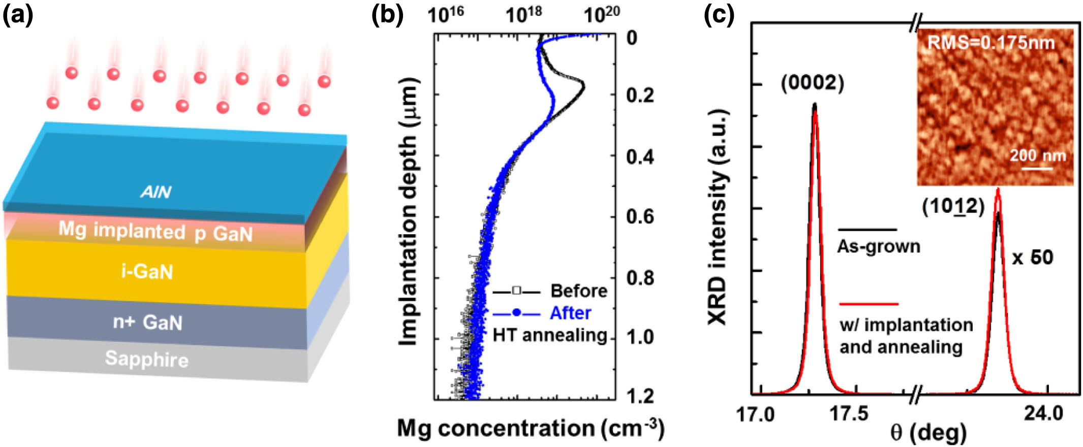
The GaN epi-structure used in this work was originally grown on sapphire substrates with MOCVD, consisting of a 1 μm undoped buffer layer, a 2 μm Si-doped n-contact layer (), and a 4 μm undoped GaN drift layer, as shown in Fig. 1(a). A 20-nm AlN capping layer was grown by atomic layer deposition (ALD) prior to the Mg implantation to protect the GaN top surface from amorphization and roughing. The Mg ion implantation was then performed at room temperature with two energy steps, 30 keV and 60 keV with doses of and , respectively. The AlN layer was then removed with TMAH solution to avoid crystallization at high temperatures. Subsequently, post-annealing for acceptor activation was performed in with a 200-nm coating layer to suppress decomposition of GaN at high annealing temperatures. And as optimized in a series of annealing experiments, a temperature of 1230°C and time of 30 min were ultimately selected as the post-activation conditions.
Sign up for Photonics Research TOC. Get the latest issue of Photonics Research delivered right to you!Sign up now
Figure 1.(a) Schematic diagram of Mg ion implantation in GaN. (b) SIMS results of Mg distribution in the GaN layer before and after annealing. (c) -ω XRD scan on (0002) and (1012) planes of as-grown GaN and Mg-implanted GaN with the post-annealing process; the inset shows the AFM morphology of GaN with Mg implantation and the post-annealing process.
After that, the GaN p-i-n photodiodes were fabricated with standard photolithography, inductively coupled plasma (ICP) etching, and electron beam evaporation. -based ICP etching was used to define individual mesa diodes and to open the contact window for the n-GaN layer prior to the ohmic contact deposition. The n-GaN ohmic contact layer composed of Ti/Al/Ni/Au (200/600/300/700 Å, 1 Å = 0.1 nm) surrounding the mesa area was then deposited and annealed at 850°C for 30 s with a rapid thermal annealing system in . Afterwards, the top ohmic contact to the p-GaN layer with the Ni/Au (100/100 Å) layer was deposited and annealed at 500°C for 5 min in air. The inset in Fig. 2(a) shows the cross-sectional schematic of the fabricated PD with an active area with a diameter of 150 μm.
Figure 2.(a) Current-voltage (I-V) characteristics of the fabricated quasi-vertical GaN p-i-n diode with a Mg implanted p-type layer; the inset illustrates the cross-sectional schematic of the diode. (b) I-V results in linear plots. (c) Electroluminescence (EL) spectrum of the Mg ion-implanted GaN p-i-n diode; the inset displays the EL emission pattern.
Based on the secondary ion mass spectroscopy (SIMS) measurement, Fig. 1(b) illustrates the Mg distribution profile after the AlN-capped implantation and -protected HT annealing. Mg concentration averaged at within a depth range of could be obtained (blue curve). As compared to the concentration distribution before annealing (black curve), a strong accumulation of Mg near the GaN surface could be observed. This should be attributed to the out-diffusion of Mg in the HT annealing process, similar to previous Mg implantation reports [12,13]. The crystalline quality of Mg-implanted GaN after activation annealing was also analyzed by high-resolution X-ray diffraction (XRD) measurements. As displayed in Fig. 1(c), the full-widths at half-maximum (FWHMs) for the GaN (0002) and (1012) XRD curves (red) are 238 and 291 arcsec, respectively. These values remain similar to those of the as-grown GaN (black), indicating the effectiveness of HT annealing on eliminating implantation-induced damage and extra strain. This is consistent with the surface morphology results as shown in the inset in Fig. 1(c), where the surface roughness of 0.175 nm over a msupmsup area is revealed with an atomic force microscope (AFM) system. Therefore, preferable recovery should have been achieved for the GaN material with the adoption of an AlN and protection layer, as well as the post-annealing treatment.
B. p-GaN Layer Recognition
Activation of the implanted Mg ion needs to be specifically verified before the demonstration of Mg ion-implantation-based GaN p-i-n photodiodes. Based on the implanted and post-treated GaN layer, a quasi-vertical diode was fabricated with the cross-sectional schematic illustrated in the inset in Fig. 2(a). Typical rectification behavior of the diode was observed in current-voltage (I-V) measurements, as shown in Figs. 2(a) and 2(b). An on-to-off ratio over at was achieved, with a turn-on voltage of extracted from the linear plots presented in Fig. 2(b), which could be expected from the bandgap of GaN [14,15].
The electroluminescence (EL) spectrum of the diode was also studied, with results displayed in Fig. 2(c). At a forward pumping current of , a peak emission at the energy of 3.26 eV was obtained. This should be a result of band-to-band radiative recombination occurring at the i-layer, with electrons and holes injected from n-GaN and p-GaN regions, respectively. More importantly, the EL pattern of the fabricated diode indicates that the radiative recombination occurs in the whole GaN diode area (solid circle), instead of being limited to the metal electrode periphery (dashed circle). On the basis of the above I-V measurements and EL mapping experiments, inversion of p-type GaN in the implanted region was validated.
C. UV Detection Characterization
In the UV detection characterizations, the RT dark current and photocurrent curves of the GaN p-i-n diode are given in Fig. 3(a), where the optical power density of the 365-nm UV front illumination is . The p-i-n diode exhibits an ultra-low dark current of at zero bias, with a photocurrent () of , exhibiting the photovoltaic mode operation capability. Figure 3(b) presents the photoresponse measurement results at zero bias (blue curve) for the GaN PD. It shows a peak responsivity of 350 mA/W at 360 nm, corresponding to an external quantum efficiency (EQE) of 120%. The responsivity spectrum also features a sharp cutoff at 365 nm, conforming to the optical bandgap energy of GaN. The UV/visible rejection ratio reaches a high value of , as defined with the 360-nm responsivity divided by that measured at 450 nm. A similar cutoff wavelength and peak position for the responsivity spectrum could be observed for a commercially available GaN p-n photodiode [16], as displayed in Fig. 3(b) with the red curve. A peak responsivity of 172 mA/W and EQE of 59% could be extracted, consistent with previously reported MOCVD grown GaN p-n-diode-based UV detectors [3,4]. Therefore, the UV PD based on the Mg ion-implanted p-i-n diode exhibits similar wavelength selectivity and photoresponsivity as compared to the commercial GaN p-n photodiodes.
Figure 3.(a) Photo- and dark current measurements for the Mg ion-implanted quasi-vertical GaN p-i-n photodiode. (b) Spectral response characteristics at zero bias of the UV photodetector based on the Mg ion-implanted p-i-n diode (blue) and a commercially available GaN p-n photodiode (red).
On the other hand, the higher EQE exceeding 100% of the Mg-implanted PD suggests towards the presence of an internal gain mechanism. This can be attributed to the trapping effects of photo-generated carriers in localized defect-related states, which then modulate the electrical conduction of the semiconductor layer with carriers injected from both electrodes to maintain charge neutrality, leading to an enhanced responsivity value [4,17]. The existence of trap-like states has been verified with the slight increase of the dark current after photocurrent measurement, as shown with the red arrow in Fig. 3(a). That is, subsequent to the photocurrent measurements, the trapped photo-generated carriers could contribute to the leakage current under dark in the following measurements.
D. Device Physics Analysis for the Mg-Implantation-Based GaN p-i-n Photodiode
To gain insight into the localized defect-related trap states in the Mg-implanted GaN vertical p-i-n diode, temperature-dependent reverse I-V characteristics were measured in the range from 290 K to 390 K. As shown in Fig. 4(a), apparent dependence of current on both the reverse bias () and temperature could be observed.
Figure 4.(a) Temperature-dependent leakage measurement. (b) Hopping conducting-based linear fitting between versus . (c) Linear fitting between and . (d) Poole–Frenkel emission-based linear fitting between and .
To identify the underlying leakage mechanism, the correlation between leakage current and electric field was explored. The average electric field at a given was estimated by , where is the drift layer thickness (μ) and is the built-in junction voltage () [18]. A linear relationship between and was found in a low bias range (), and is valid at various measuring temperatures, as shown in Fig. 4(b). This reveals the hopping-related carrier transport mechanism under low reverse bias conditions, consistent with the conclusions of previous related research [18–20]. Thus, current-field dependence could be described by [18–20]where is the Boltzmann constant, is the temperature, is a characteristic temperature parameter, is the zero-field current, is the electron charge, is a constant of unity, is the average hopping distance between two trap states, and is the slope of versus . Using Eq. (1) to fit the experimental data of J-E, as shown in Fig. 4(b), could be obtained. Figure 4(c) illustrates the linear fitting of versus , based on which the corresponding slope of could be extracted to be . Assuming a localization radius Å and , could be extracted to be . The localized states density supporting the hopping conduction could then be estimated by [20,21], with a value of , even lower than the previously reported sapphire-based GaN, which has not experienced the implantation and HT annealing process [18]. The similar dominant leakage mechanism and localized trap-state density indicate that the optimized post-annealing treatment could effectively repair the ion-implantation-related lattice damage and evidently recover the material quality. This agrees well with the comparable UV photodetection performances between these Mg-implantation-based GaN p-i-n photodiodes and commercially available GaN p-n PDs grown by MOCVD.
The energy obtained by a hopping carrier within a hopping distance () would increase with the enhanced electric field (). Therefore, with increasing reverse bias, carriers could get enough energy to escape from the localized states when the obtained energy extends the energy gap () between localized states and the band barrier. Then, the Poole–Frenkel (PF) emission would be stimulated. Figure 4(d) displays the linear fitting of versus the square root of the electric field with reverse bias over 20 V. A typical PF conduction relationship is given as [22,23]where is the PF constant, is the vacuum permittivity, and is the dielectric permittivity of GaN (). Near-ideal linear PF conduction fitting was observed for various values. The PF constant was then calculated to be , in good consistency with the theoretically predicted value of . The dominance of PF emission at high reverse bias was then verified, further confirming the existence of localized states.
The identification of hopping conduction as well as the PF emission process also indicates that the photo-generated carriers trapped in the localized states could spatially hop or transit between these states, enhancing the charge non-neutrality and thus increasing the photoresponsivity. This process would be intensified with higher electric field intensity. This has been verified by the results of responsivity versus , as shown in Fig. 5(a). Responsivity increases near exponentially with and exhibits a sharp increase near , where leakage starts to exhibit clear linear fittings with hopping conduction, in good consistency with results presented in Fig. 4(b), where . Meanwhile, the linearity between photocurrent and incident optical power density has excluded the dominance of an undesired persistent photoconductivity mechanism in the fabricated UV PDs, as presented in Fig. 5(b)[4,17].
Figure 5.(a) Reverse-bias-dependent responsivity measurement at an optical power density of at 365 nm. (b) Dependence of photocurrent on the optical power density. (c) Schematic diagram of the electric-field-assisted photocarrier hopping.
The transient photoresponse characteristics have been evaluated at the reverse bias of 5 V, employing a 325 nm constant-wave (CW) laser with optical power density of , and a frequency-programmable chopper. The photocurrent waveform in six repeated cycles with a chopping frequency of 140 Hz is presented in Fig. 6(a). The photocurrent was observed to be consistent and repeatable in the continuous measurements. 10% to 90% of the maximum value was used for the extraction of response time [24–27], as shown in Figs. 6(b) and 6(c). The rise time () and decay time () are estimated to be 75 μs and 110 μs, respectively.
Figure 6.Time response characteristics of the Mg ion-implantation-based GaN p-i-n diode. (a) Response waveform in six repeated circles. Photocurrent (b) rise and (c) decay edge within one response pulse. (d) Decay waveform in exponential scale.
Based on the junction capacitance and forward series resistance of the p-i-n diode, the RC time constant () is estimated to be , and therefore should not be the main factor influencing the photoresponse time. Thus, it is believed that the photoresponse time obtained here should be determined mainly by the injection and depletion process of the trapped carriers in localized states. As displayed in Fig. 6(d), the near exponential decay of the photocurrent further excludes the dominance of the persistent photoconductivity effect [4,17].
In consideration of both the photoresponsivity’s dependence on the reverse bias and the transient response characteristics, a physics model of electric-field-assisted photocarrier hopping is proposed: the photocarriers first get trapped in the localized states, introducing non-neutrality in the GaN drift region, causing EQE extending 100%; these captured carriers then hop or transit spatially in the localized states with the assistance of an applied electric field, further enhancing the photoresponsivity, as clarified in Fig. 5(c). Therefore, for the Mg-implantation-based GaN p-i-n UV photodiode demonstrated in this work, suppression of localized trap states in GaN and low-bias operation mode would be favorable in alleviating the influences of a parasitic internal gain mechanism.
4. SUMMARY
A GaN p-i-n diode for UV photodetection based on the Mg ion-implanted p-GaN layer was demonstrated in this work. During the implantation and activation of the Mg ion, an AlN and protective layer was proved to be efficient for reducing lattice damage in high-energy implantation and the HT annealing process, respectively. Resultantly, a p-type GaN layer and corresponding quasi-vertical GaN p-i-n diode with excellent rectification performance was achieved. Subsequent photoresponse characterizations revealed its good overall visible-blind UV detection performances, including sharp spectrum cutoff at 365 nm with a UV/visible rejection ratio over , photoresponse time at a level of μ, and high detection linearity. Meanwhile, an internal gain mechanism was observed and proved to be related to the localized states within the drift layer. Resultantly, a physics model with field-assisted hopping of photo-generated carriers was proposed. It is believed that this study will promote the understanding of UV PD device physics in Mg ion-implantation-based GaN p-i-n diodes and provide a new CMOS compatible strategy for high-performance GaN p-i-n UV photodiode fabrication toward practical applications.
[13] N. E. Posthuma, S. You, H. Liang, N. Ronchi, X. Kang, D. Wellekens, Y. N. Saripalli, S. Decoutere. Impact of Mg out-diffusion and activation on the p-GaN gate HEMT device performance. 28th International Symposium on Power Semiconductor Devices and ICs (ISPSD), 95-98(2016).
[19] Y. Zhang, H. Y. Wong, M. Sun, S. Joglekar, L. Yu, N. A. Braga, R. V. Mickevicius, T. Palacios. Design space and origin of off-state leakage in GaN vertical power diodes. IEEE International Electron Devices Meeting (IEDM), 1-35(2015).