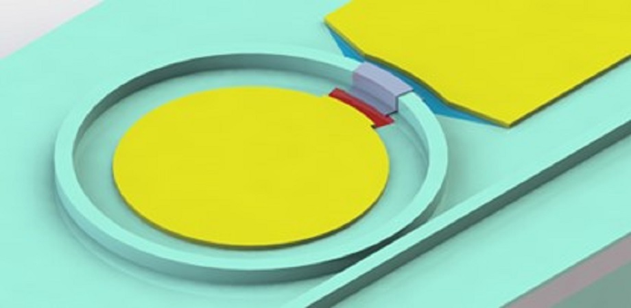
New approach to photonic memory integrates a phase-change material to enable in-situ training of optical neural networks. Credit: Maoliang Wei and Kai Xu.
Technological advancements like autonomous driving and computer vision are driving a surge in demand for computational power. Optical computing, with its high throughput, energy efficiency, and low latency, has garnered considerable attention from academia and industry. However, current optical computing chips face limitations in power consumption and size, which hinders the scalability of optical computing networks.
Thanks to the rise of nonvolatile integrated photonics, optical computing devices can achieve in-memory computing while operating with zero static power consumption. Phase-change materials (PCMs) have emerged as promising candidates for achieving photonic memory and nonvolatile neuromorphic photonic chips. PCMs offer high refractive index contrast between different states and reversible transitions, making them ideal for large-scale nonvolatile optical computing chips.
While the promise of nonvolatile integrated optical computing chips is tantalizing, it comes with its share of challenges. The need for frequent and rapid switching, essential for online training, is a hurdle that researchers are determined to overcome. Forging a path towards quick and efficient training is a vital step on the journey to unleash the full potential of photonic computing chips.
Recently, researchers from Zhejiang University, Westlake University, and the Institute of Microelectronics of the Chinese Academy of Sciences achieved a breakthrough. As reported in Advanced Photonics, they developed a 5-bit photonic memory capable of fast volatile modulation and proposed a solution for a nonvolatile photonic network supporting rapid training. This was made possible by integrating the low-loss PCM antimonite (Sb2S3) into a silicon photonic platform.

Optical convolution kernel based on the volatile-modulation-compatible photonic memory: (a) Schematic architecture of a 4×4 OCK. The inset is the discrete device of OCK. (b) The nonvolatile multi-level switching of photonic memory. (c) The volatile modulation dynamic response of the photonic memory. (d) Schematic diagram of the on-chip training and writing operation of the OCK. (e) The prediction accuracy after simulated in-situ training of the OCK. (f) The prediction accuracy after the simulated memorizing of photonic memory of the OCK. Credit: M. Wei et al., doi 10.1117/1.AP.5.4.046004
The photonic memory utilizes the carrier dispersion effect of a PIN diode to achieve volatile modulation with a rapid response time of under 40 nanoseconds, preserving the stored weight information. After training, the photonic memory utilizes the PIN diode as a microheater to enable multilevel and reversible phase changes of Sb2S3, allowing the storage of trained weights in the photonic computing network. This leads to an incredibly energy-efficient photonic computing process.
Using the demonstrated photonic memory and working principle, the research team simulated an optical convolutional kernel architecture. Remarkably, they achieved over 95 percent accuracy in recognizing the MNIST dataset, showcasing the feasibility of fast training through volatile modulation and weight storage through 5-bit nonvolatile modulation.
This groundbreaking work establishes a new paradigm for photonic memory and offers a promising solution for implementing nonvolatile devices in fast-training optical neural networks. With these advancements, the future of optical computing looks brighter than ever before.
Read the Gold Open Access article by M. Wei et al., “Electrically programmable phase-change photonic memory for optical neural networks with nanoseconds in situ training capability,” Adv. Photon. 5(4) 046004 (2023), doi 10.1117/1.AP.5.4.046004