Advanced microscale silicon photonics technology has emerged as a promising candidate for the next-generation chip-scale data communication network due to its unique advantages of low cost, high integration density, high speed and energy efficient. However, a highly efficient microscale Si-based light source is still considered as the obstacle for realizing a practical Si-based photonic integrated circuit (PIC), due to the indirect bandgap nature of bulk Si and Ge materials.
Various approaches towards integration of microcavity lasers on Silicon substrates have been demonstrated extensively, including co-packing, hybrid integration, wafer bonding, etc. But these methods more or less include cumbersome fabrication process. Monolithic integration method, however, is another promising route towards low cost and scalable Si-based PICs. Because monolithic integration takes advantages of advanced fabrication process of contemporary integrated circuits, in other words, it is unnecessary to consider heterogeneous way to make precise alignment between light source and other optical components. Nevertheless, the fundamental challenge of epitaxial III-V on Si is the degraded material quality caused by large material dissimilarities. The planar defect, anti-phase boundary, due to the polar on non-polar growth, can be avoided by employing pretreated double-atomic-step Si substrate. Furthermore, strained-layer superlattice (SLS) has been used as defect filter layers to significantly reduce the threading density defect caused by the lattice mismatched heteroepitaxial growth of III-V materials on Si. In addition, semiconductor lasers with quantum dots (QDs) as gain material have been extensively investigated due to its robust tolerance to defects, which is significant to PIC.
The research group led by Professor Zhaoyu Zhang from The Chinese University of Hong Kong, Shenzhen demonstrated InAs/GaAs QD square-lattice photonic crystal bandedge lasers monolithically grown on on-axis Si (001) substrates. The lasers operated under continuous-wave optical pumping at room-temperature. Ultra-low lasing threshold was observed in a multi-mode lasing operation(Fig. 1). The research results are published in Chinese Optics Letters, Volume 20, No. 4, 2022 (Yaoran Huang, et al. Highly integrated photonic crystal bandedge lasers monolithically grown on Si substrates.)
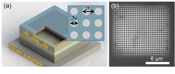
Fig. 1. (a) A schematic diagram of the fabricated InAs/GaAs QD bandedge laser directly grown on on-axis Si (001) substrate. The lattice constant and radius of air holes are a and r, respectively. (b) A SEM image of fabricated photonic crystal bandedge cavity with the parameters of r/a = 0.35 and the slab thickness 1.05a.
In this work, they demonstrated InAs/GaAs QD square lattice photonic crystal bandedge lasers monolithically grown on on-axis Si (001) substrate with ultra-low lasing threshold under 632.8 nm He-Ne gas laser source at room temperature. The fabricated photonic crystal slab in this work utilizes the band-edge effect of photonic crystals to achieve in-plane light resonance. By tuning the structural parameters of the band-edge photonic crystals, photonic crystal surface-emitting lasers (PCSELs) with a much smaller footprint can achieve precise wavelength control and mode field confinement, and finally achieve a higher quality factor than conventional vertical-cavity surface-emitting lasers (VCSELs). The far-field pattern with Gaussian-like distribution from PCSEL is easier to be coupled into single-mode fiber, which is beneficial to realize silicon photonics, gas sensing and other related applications. In order to further enhance the selection and confinement of optical modes, the optical band gap (PBG) effect of photonic crystals may be utilized to design point defects or line defects within the photonic crystals, enabling selection of defect modes with different symmetries by destroying its periodic structure.
The corresponding mode will be localized near the defect center, thereby achieving controllable emission direction, low divergence angle and higher output power. The narrow linewidth of PCSEL makes it possible to greatly reduce modal dispersion and transmission loss during transmission after subsequently coupling to a single-mode waveguide. Therefore, this square-lattice photonic crystal band-edge laser is expected to become a coherent light source for large-scale monolithic integrated silicon photonics systems in the future.