Researcher Yufang Zhe's group from the School of Physics, Peking University published a review article (Yijing Huang, et al. Engineering of single-photon emitters in hexagonal boron nitride [Invited]) in Chinese Optics Letters , Vol. 20, No. 3, 2022. System introduction The preparation, optimization methods, integration and application of hexagonal boron nitride single-photon emitters are presented, and a summary and outlook are made, which are selected as the current Editors' Pick.
1. Introduction
Quantum information technology requires bright and stable single-photon emitters (SPEs). Since the first observation of the quantum emission from hBN monolayers at room temperature, SPEs in hBN have attracted extensive attention due to their fascinating optical properties, such as ultra-high brightness, absolute photostability, and robustness to harsh chemical conditions. As the most common 2D material except for graphene, owing to the high mechanical strength and flexibility, hBN can be well integrated with cavities, photonic waveguides, and plasmonic structures. Further investigations have revealed that hBN is a natural hyperbolic material in the mid-IR range and offers strong UV emission at the same time. Because hBN has a unique combination of optical properties and can realize novel nanophotonic functionalities, growth technologies related to hBN are booming. Recent advances in these areas make it possible to explore in-depth the engineering and tuning of room-temperature SPEs in hBN.
2. Fabrication and regulation of Quantum Emitters in HBN
2.1 Fabrication and Optimization of SPEs in HBN
Chemical Vapor Deposition Growth Method
In a recent investigation of CVD, a bottom-up fabrication of hBN using low-pressure chemical vapor deposition (LPCVD) is proposed. This technique can be used to prepare centimeter-scale, few-layer hBN films that host a high density of bright, uniform, and photostable SPEs on copper, nickel, and iron substrates. Based on that, a further study puts forward an effective method to produce quantum emitters in hBN with desired emission properties in different spectral regions by boron diffusion through copper via boron during atmospheric pressure chemical vapor deposition(APCVD). Besides, a recent investigation demonstrated that the CVD process based on Pt catalyst can realize the controlled growth of large monolayer hBN, and can also peel off the grown films directly from the catalyst to realize the cleaning process. This approach can achieve precise control of hBN thickness. Subsequent further exploration revealed that SPEs are selectively incorporated only in hBN grown on (001) Ni. Another recent study demonstrates a positive approach to spatially control generation of hBN SPEs. Specifically, hBN is directly grown onto dielectric nanopillars by CVD growth method.
Proper Surface Passivation
A recent work explored a novel method based on atomic layer deposition (ALD) of a 2nm thin spacer layer between and the hBN, ameliorating the problem of blinking and spectral diffusion in narrowband quantum emitters.
Focused Ion Beam (FIB)
SPEs can be deterministic placed by using a gallium FIB patterned milling of hBN to create edges. By optimizing milling and annealing parameters, a 31% yield of SPEs is obtained. This FIB-based manufacturing approach meets the critical need to create and control SPEs in hBN, thus being able to integrate these SPEs into chip-scale plasmonic, photonic, and optomechanical devices for quantum information applications at room temperature, greatly expanding the potential applications of SPEs.
In addition, there are a series of processing methods such as plasma etching, chemical etching, electron beam irradiation, ion irradiation, neutron irradiation and Ultraviolet (UV) ozone processing, which can increase the probability of SPEs formation and optimize the performance of SPEs to a certain extent.
2.2 Introduced External Fields to Regulate the Quantum Emission of hBN
Strain Engineering
Superior high mechanical strength and flexibility of hBN allow tuning physical and optical properties by strain engineering effectively. Because of the strong in-plane atomic bonds in 2D materials, external strains can be applied to change the electronic energy levels of fluorescent defect states. For instance, the biaxial strain affects the electronic properties of carbon defects in hBN monolayers. Another theoretical work also pointed out that the bandgap of hBN was adjustable by applying strain because the interlayer distance between two layers in the hBN double layers could be changed under the applied strain. When it comes to uniaxial tension (for two to four layers of hBN flakes), large shifts and splitting of the E2g phonon are observed, and the phonon shift rates are sensitive to strain.
Bending of a flexible substrate is a common technique to induce strain. As illustrated in Fig. 1(a), when the strain is changed, the maximum spectral tunability of hBN SPEs can reach more than 6meV. Interestingly, when the pressure-dependent PL spectra of hBN flakes are measured at low temperatures, three different types of pressure responses can be found, namely redshift (negative pressure coefficient), blueshift (positive pressure coefficient), and sign change from negative to positive, as shown in Fig. 1(b). Lately, new advances have been made in applying tensile strain to SPEs embedded in several layers of hBN films and achieving both red and blue spectral shifts with tuning amplitudes up to 65meV.
In addition to tuning the ZPL spectrum of hBN, strain engineering can also be used to determinatively activate SPEs in the hBN. Defects are activated by nanoscale strain engineering of several atomic layers of hBN flake (about 20nm thick) using nanopillar substrates, as shown in Fig. 1(c). This work sets a foundation for the realization of room-temperature single-photon source arrays by combining strain and external electrostatic potential. It has been reported that the density of SPEs in hBN is related to the perimeter, so quasi-one-dimensional boron-nitride nanotubes (BNNTs) with rich curvature have received much attention, as shown in Fig. 1(d). It shows a linear relationship between the energies of the emitted single photon and the external forces imposed on the (7,0) NBVN @BNNTs, which can be used as an ideal high-precision force detector.
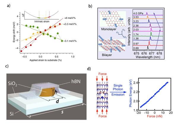
Figure 1 Strain engineering of SPEs in hBN. (a) The curve shows the scaled energy shift as a function of applied strain to the bendable substrate for three emitters with different tunability of −3.1meV/% (green), + 3.3meV/% (yellow), and + 6meV/% (red). (b) Schematic diagrams for the strain applied in monolayer (upper part) and bilayer (lower part) geometries and the pressure-dependent PL spectra of hBN flakes at low temperatures by using a diamond anvil cell device. (c) A wet transfer using a ∼20 nm-thick flake of hBN on a nanostructured silica substrate. (d) The relationship between the energies of the emitted single photon and the external forces imposed on the (7,0) NBVN@BNNT.
Electrical Control
The Stark effect, which describes the regulation of the emitted photon energy via shifting the electron energy level by an external electric field, is easily integrated into a quantum system, which has advantages over other tuning methods such as strain field. A nanoscale four-electrode device is designed, which can not only control the direction of the electric field but also achieve an unprecedented in-plane field on the order of 0.1V/nm, orders of magnitude higher than previous reports using similar in-plane electrode design, as shown in Fig. 2(a). Similarly, in the van der Waals graphene/hBN/graphene heterostructures, the single-photon emission of atomic defects in hBN can be electrically controlled by the Stark effect. HBN flakes (100 ~200nm) are sandwiched by the top and bottom few-layer graphene, as shown in Fig. 2(b). When a varying vertical electric field is applied to the device, a shift in the center wavelength can be observed at both 10K and room temperature. Besides, a method of effectively introducing electrostatic field and realizing large and reversible Stark-shift tuning of SPEs in hBN is introduced, as shown in Fig. 2(c). By applying a voltage between the two, a large reversible spectral shift of (5.5±0.3) nm per GV/m is observed. This method of individual control and reversible adjustment of SPEs in hBN using a high-resolution conductive AFM tip can be applied to accurately determine the SPE position.
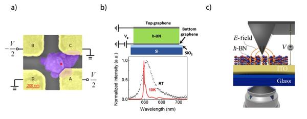
Figure2 Electrical Control of SPEs in hBN. (a) Device of the Stark effect in hBN SPE at room temperature. A, B, C, and D (yellow) denote the four gold electrodes where voltages are applied to generate external electric fields. (b) Device schematics of multilayer hBN sandwiched by the top and bottom few-layer graphene and PL spectrum of the emitter shown in panel b measured at 10K and room temperature. (c)Schematic representation of the experiment. An hBN flake is located on an ITO-covered glass substrate.
Temperature Dependence
Recent studies have discussed the temperature dependence of the broadened homogeneous and inhomogeneous components and demonstrated that the spectral emission linewidth of CVD-grown and exfoliated crystals on conductive ITO decreases with temperature relative to those seen on SiO2 substrates. This study found that the emitter line width is both temperature-dependent and temperature-independent, which are attributed to thermally phonon interactions and spectral diffusion, respectively, which are responsible for ZPL emission broadening. Based on the sensitive temperature correlation in hBN, a deterministic optical temperature measurement technique based on SPEs in hBN is proposed in the subsequent research. These nanothermometers exhibit better performance in sensitivity and wide operating temperature range than other optical nanothermometers. Taking the chromium microcircuit, the function of monitoring temperature at multiple target locations can be achieved by measuring the PL of three hBN nanoflakes transferred to it. This work offers more possibilities for nanoscale temperature measurements and heat flow research in micro and nano-integrated devices.
Photoinduced Modification
A recent work achieves a controlled optical switch between the light and dark states of the color centers that emit about 2eV, These results are beneficial to the experimental study of enhancing the PL yields, especially under resonance excitation, and can play an important role in the color center recognition of hBN.
Magnetic Field Dependence
Recently, it has been reported that individual SPEs with spin-dependent optical properties in hBN can be identified and characterized. This work demonstrated that the SPEs in hBN show the room-temperature and magnetic field associated PL properties, which are consistent with the spin-dependent inter-system crossing transitions, paving the way for the development of 2D quantum spintronics.
Acoustical Modulation
Lately, the effect of surface acoustic waves (SAWs) on the light emission from the defect center in the hBN was investigated. For hBN flakes, it is demonstrated that the modulation of emission lines by alternating acoustic fields and estimated a deformation potential for defects of about . It is shown that tuning SAWs is an effective way to regulate and control the electronic states of 2D materials.
3. Integration and Application Based on HBN
3.1 Photonic and Plasmonic Nanostructures
In the pioneering work of a hybrid quantum 2D material system integrated with plasmonic nanocavity arrays, the quantum emitters in the hBN were determinatively coupled to plasmonic gold and silver arrays with high quality, and the coupled emitters showed better performance, as shown in Fig. 3(a). In another work, similar conclusions are obtained and the good coupling between quantum emission in hBN and the surface lattice resonance modes of silver nano-pillar arrays is also realized. In addition to metal nanoarrays, the tip of an atomic for AFM can be used to precisely locate the gold nanospheres next to SPEs. The controllable nanoscale assembly can also result in enhanced emission and reduced lifetime of the SPEs in hBN. On this basis, a scheme of embedding hBN SPEs into the chip array of the metal-dielectric antenna is proposed, which can provide nearly uniform light collection efficiency, the experimental value is up to 98%, 7 times higher than the bare SPEs, as shown in Fig. 3(b). In the latest research, a near field coupling between hBN SPEs and a resonant plasmonic nanoantenna is proposed. Since this work quantifies the luminescence intensity and luminescence lifetime associated with the antenna position (nanoscale), it is possible to induce hBN defects deterministically at positions determined within the hBN-layer.
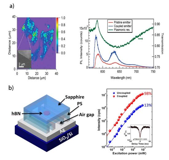
Figure 3 Optical coupling systems between SPEs and plasmonic nanostructures. (a) PL confocal map and PL spectra of a flake containing SPEs (red circled). Inset, SEM image of part of the flake on top of the gold plasmonic lattice. (b) Schematic of the on-chip MDA device. Spectrally integrated PL intensity versus pump power for the uncoupled (blue data points) and coupled state (red data points). Inset: Emitter intensity over time showing excellent temporal stability without blinking.
3.2 Dielectric Optical Cavities and Waveguides
A recent investigation proposes on-chip integration of hBN quantum emitters with photonic crystal cavities from . The hBN/ hybrid cavities can achieve an experimentally measured quality factor of 3300 and the six-fold PL enhancement of hBN single-photon emission at room temperature. The coupling of another microcavity structure with hBN flakes can fully suppress phonon sideband and other non-resonant noises, as well as greatly enhance the directivity and spontaneous emission rate of quantum emission. The microcavity can be easily adapted to other quantum emitters in 2D materials and provides new hope for scalable quantum information processing platforms. In addition to the short waveguides on the nano- and micro-scale mentioned above, the research on the integration of hBN emitters with optical fibers has made great progress in recent years, which is more important for remote applications such as quantum communication. The light emitted by a SPE into the optical fiber can be collected effectively, and it is proved that when the light is guided through the optical fiber, the quantum properties of light remain unchanged , as shown in Figure 4. The coupling of a quantum emitter in hBN to a tapered fiber was demonstrated and the collection efficiency of the system was 10%. Good coupling efficiency with tapered fiber even allows excitation and detection in a fully fiber-coupled manner, resulting in a truly integrated system. In subsequent studies, the SPEs in hBN are coupled to a hybrid system based on an optical fiber-based Fabry–Pérot cavity. This hybrid platform operates in a wide spectral range greater than 30nm and can be used to explore different coupling regimes. The cavities used in this work exhibit a high fineness of up to 3000 and small modal volume down to or lower for , making them ideal for coupling to hBN SPEs. In addition, the cavity-assisted PLE spectroscopy mentioned in this work can be used to characterize mechanically isolated defect centers in hBN at room temperature in the future with critically enhanced photon flux.
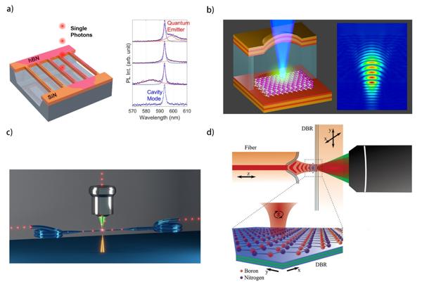
Figure 4 Optical coupling systems based on SPEs in hBN. (a) Schematic of the on-chip integration of hBN quantum emitters with photonic crystal cavities from silicon nitride (). PL spectra, without normalization showing PL enhancement of the emitter. (b) The microcavity consists of a hemispherical and flat mirror (only 2 stacks shown on either side). The quantum emitter hosted by hBN emits confocally with the excitation laser. (c) Schematic diagram of a device coupling a quantum emitter to an optical fiber. (d) Schematic design of micro resonator device. The planar resonator is composed of a macroscopic plane mirror and a glass fiber tip with a concave structure. The hBN film grown by CVD is placed on the plane mirror to form a hybrid quantum emitter fiber-cavity system.
In addition to 2D material systems, there have been several studies looking at lower dimensional systems. For example, bright visible light SPEs have been found in a zero-dimensional boron nitride allotrope (the boron nitride nanococoon, BNNC). This discovery has led to the development of super-bright, stable, solid-state single-photon sources. In addition, a bottom-up technique for the fabrication of sub-10-nm hBN nanoparticles hosting photostable bright SPEs via a catalyst-free hydrothermal reaction between boric acid and melamine is demonstrated. This study presents a promising strategy for the scalable, bottom-up synthesis of high-quality SPEs in hBN nanoparticles.
3.3 Future Applications Based on hBN
A recent work details the creation of single photon randomness of SPEs in hBN. In this way, quantum random number generation with SPEs does not rely on any beam splitting optics, and the rates could be increased by two times compared to the beam splitter dependent architecture. In the future, this scheme has potential application prospect in quantum communication.
A recent work uses a quantum light source based on a color center in hBN coupled to a microcavity to test higher-order interference. It is proved that the nonlinearity of the detector is completely avoided by using a single photon source and the tight bounds of high order interference are obtained. In short, in the direction of photon quantum technology and coherent control, the exploration work based on hBN single photon sources provides more possibilities for the realization of multifunctional optical quantum technology in the future.
4. Conclusion
The origin of hBN quantum emission is still under debate. In actual scenarios, the heterogeneity of the hBN structure leads to the diversity of hBN defects, which makes it more difficult to explore the emission mechanism of hBN. In the future, more attention should be paid to how to adapt SPEs in hBN to large-scale or industrial applications with more accessible processes. To date, devices based on hBN SPEs have been able to achieve some functions, such as precision optical temperature measurement, high precision, and high sensitivity force measurement, etc. The development of physical principles and phenomena in quantum emission in hBN is vigorous. With the deepening of the research in hBN quantum optical properties, more and more chances for hBN-based hybrid integration in quantum devices may emerge.