• Chinese Optics Letters
  • Vol. 20, Issue 3, 032701 (2022)
Yijing Huang, Zhibo Dang, Xiao He, and Zheyu Fang*
Author Affiliations
  • School of Physics, State Key Laboratory for Mesoscopic Physics, Academy for Advanced Interdisciplinary Studies, Collaborative Innovation Center of Quantum Matter, and Nano-optoelectronics Frontier Center of Ministry of Education, Peking University, Beijing 100871, China
  • show less
    DOI: 10.3788/COL202220.032701 Cite this Article Set citation alerts
    Yijing Huang, Zhibo Dang, Xiao He, Zheyu Fang. Engineering of single-photon emitters in hexagonal boron nitride [Invited][J]. Chinese Optics Letters, 2022, 20(3): 032701 Copy Citation Text show less

    Abstract

    Quantum information technology requires bright and stable single-photon emitters (SPEs). As a promising single-photon source, SPEs in layered hexagonal boron nitride (hBN) have attracted much attention recently for their high brightness and excellent optical stability at room temperature. In this review, the physical mechanisms and the recent progress of the quantum emission of hBN are reviewed, and the various techniques to fabricate high-quality SPEs in hBN are summarized. The latest development and applications based on SPEs in hBN in emerging areas are discussed. This review focuses on the modulation of SPEs in hBN and discusses possible research directions for future device applications.

    1. Introduction

    Over the past decades, the field of non-classical light sources has expanded exponentially, tightly related to the fields of quantum photonics, super-resolution imaging technology, and quantum information science, which specifically includes quantum key distribution, quantum computation, quantum communication, and precision sensing. In the experimental foundation of quantum mechanics[1] and measurement theory[2,3], the generation and detection of non-classical photons also play an important role. The quantum-photon property of quantum communication helps prevent the interception of encoded information, ensuring the privacy of communication. Therefore, the production of robust, bright, and indistinguishable quantum emitters is an important prerequisite for the creation of photon qubits for effective quantum communication[4]. Moreover, due to the high-speed transmission and excellent noise characteristics of photons, the field of quantum photonics is very active in recent years, which also requires the solutions of the on-demand activation of single-photon sources and the compatibility of devices[5].

    Although there is still no ideal quantum emitter satisfying industrial production, quite a few quantum emitters in solid-state systems have been transformed from theoretical prediction to engineering design and optimized performance, such as color centers in crystals, quantum dots, carbon nanotubes, 2D materials, and other solid-state host materials[6]. The optical extraction efficiency of these single-photon emitters (SPEs) can be high. Besides, owing to the high mechanical strength and flexibility, 2D materials can be well integrated with cavities, photonic waveguides, and plasmonic structures (nanometer-scale proximity). In brief, the unique properties of 2D materials make them well-suited for many applications in the field of quantum information science.

    Since the first observation of the quantum emission from hexagonal boron nitride (hBN) monolayers at room temperature[7], SPEs in hBN have attracted extensive attention due to their fascinating optical properties, such as ultra-high brightness, absolute photostability, and robustness to harsh chemical conditions. As the most common 2D material except for graphene, hBN can be assembled into heterostructures, where the monolayers are held together by the van der Waals forces[8,9]. Many studies have shown that hBN substrates and encapsulation can improve the electronic properties of graphene devices[1012]. Such devices have the potential for high-frequency operation and large-scale integration[13]. Further investigations have revealed that hBN is a natural hyperbolic material in the mid-IR range and offers strong UV emission at the same time. Because hBN has a unique combination of optical properties and can realize novel nanophotonic functionalities, growth technologies related to hBN are booming[14,15]. Recent advances in these areas make it possible to explore in-depth the engineering and tuning of room-temperature SPEs in hBN.

    In this review, research on the generation, properties, control, and applications of the quantum emitters in hBN is reviewed. Recent progress towards mechanism research of quantum emission in hBN is introduced. Multi-angle fabrication and coordination of SPEs in hBN are discussed. Next, the progress towards related applications is enumerated, respectively, such as integrating SPEs in hBN with photonic or plasmonic nanostructures, dielectric optical cavities, and waveguides. Lastly, the opportunities and challenges for SPEs in hBN are summarized, and new possibilities that are being explored at present and may be explored in the future are discussed.

    2. Mechanism of Quantum Emission in hBN

    The ideal SPE, as an isolated quantum system, that emits one photon at a time per excitation cycle needs to be satisfied, which is triggered optically or electrically[
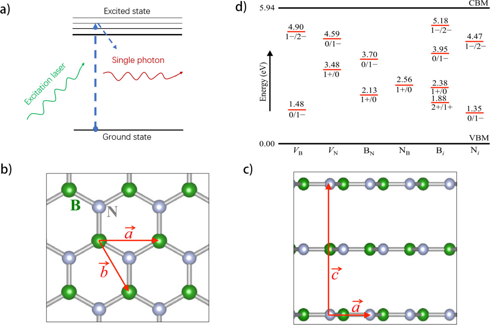
16,17]. SPE is assessed by indirect measurement of photon correlation functions, usually experimentally using Hanbury Brown and Twiss (HBT) interferometry[18]. Figure 1(a) illustrates the brief concept of SPEs, where a green laser excites a quantum system (non-resonantly) to a higher vibrational state. After ultrafast nonradiative relaxation to an excited (electronic) state, a photon is emitted as the system relaxes to its ground state. SPE results in non-Poisson photon statistics, and g(2)(τ) exhibits a dip at zero delay time, confirming the quantum nature of the detected light[19]. At the delay time τ=0, the ideal SPE g(2)(0)=11/N, where N is the number of emitters. In fact, due to the photon counts background and finite response time of the correlation measurements being limited today by the convolution of the time response of the two single-photon detectors, g(2)(0)0 in the case of the SPE. The purity of the SPE will be given by the value of g(2)(0). Note that normalization to one at longer delay times is critically important to provide accurate results[14].

    Measurement of quantum emission and structures of hBN. (a) Simple energy level diagram for quantum emission. When a quantum system is excited by light or electricity, the energy conversion between the excited state and the ground state can produce a single photon. (b), (c) The top-down and side views illustrating the in-plane honeycomb structure of hBN as well as the interlayer distance and stacking mode. B atoms and nitrogen atoms are represented in green and gray spheres. Within the (0001) plane, each N atom is threefold coordinated to B and vice versa in a honeycomb pattern that is a result of sp2 bonding. Out of the plane, hBN exhibits AA’-type stacking with alternating B and N atoms along with the [0001] direction. The interlayer separation is determined by the van der Waals interaction[15]. Copyright 2018, American Physical Society. (d) Charge-state transition levels for native point defects in hBN[15]. Copyright 2018, American Physical Society.

    Figure 1.Measurement of quantum emission and structures of hBN. (a) Simple energy level diagram for quantum emission. When a quantum system is excited by light or electricity, the energy conversion between the excited state and the ground state can produce a single photon. (b), (c) The top-down and side views illustrating the in-plane honeycomb structure of hBN as well as the interlayer distance and stacking mode. B atoms and nitrogen atoms are represented in green and gray spheres. Within the (0001) plane, each N atom is threefold coordinated to B and vice versa in a honeycomb pattern that is a result of sp2 bonding. Out of the plane, hBN exhibits AA’-type stacking with alternating B and N atoms along with the [0001] direction. The interlayer separation is determined by the van der Waals interaction[15]. Copyright 2018, American Physical Society. (d) Charge-state transition levels for native point defects in hBN[15]. Copyright 2018, American Physical Society.

    In order to design high-quality quantum emitters in hBN, it is necessary to have a clear understanding of the atomic structure in hBN and the associated excitation processes that give rise to the quantum emission. hBN is a highly anisotropic crystal, consisting of B and N atoms strongly bonded in the in-plane direction. The B–N bond is polar covalent because of the difference in electronegativity between B and N[14]. The bulk crystal structure of hBN is shown in Fig. 1(b). Native defects in hBN include boron (B) vacancy (VB), nitrogen vacancy (VN), B antisite (BN), nitrogen antisite (NB), B interstitial (Bi), and nitrogen interstitial (Ni). Figure 1(c) illustrates the charge-state transition levels for these native point defects in hBN. These defects in hBN tend to have fairly high formation energies and, in the absence of impurities, cannot form in large concentrations under thermodynamic equilibrium. hBN is commonly synthesized through mechanical[20], liquid-phase exfoliation[21], molecular beam epitaxy (MBE)[22,23], or chemical vapor deposition (CVD)[24]. During the growth of hBN, native defects are thus readily formed in an uncontrolled way, and they can be unintentionally generated to modify the structure and properties of hBN. Besides native defects, certain impurities [carbon, oxygen (O), and hydrogen impurities in common] are also likely to be present unintentionally in the growth environment, and it is important to assess whether they can be incorporated during growth. Because of the uncontrollability of impurities, so far, there has been no feasible way to generate quantum emitters at specific wavelengths in deterministic locations. The emission frequencies of the quantum emitters in hBN range from UV to near IR[7,25,26]. The emitters are often grouped according to their zero-phonon line (ZPL) energies and phonon sideband shapes[27]. Different groups of emitters possibly correspond to chemically different defects, defects with different charge states, or a combination of both. Even for what appears to be the same defect in a sample, a large spectral distribution in the ZPL frequencies is reported[28,29]. Based on the research progress of quantum emitters in hBN, the emission frequencies in the two ranges of 2 eV and 4.1 eV are mainly discussed below.

    2.1. 2 eV luminescence

    When quantum emission at 623 nm from localized defects in hBN monolayers and multilayers at room temperature was first discovered, it showed extremely high brightness (I4.2×106countss1 at Psat611μW) and light stability[7]. The hBN SPE was analyzed in the frame of an extended three-level model, which was used in plenty of subsequent studies[3034]. The g2(τ) is given by Eq. (1), where τ1 and τ2 represent the radiative transition lifetime and the metastable-state lifetime, respectively, and a is a photon bunching factor: g2(τ)=1(1+a)e|τ|τ1+ae|τ|τ2.

    Density function theory (DFT) was used to investigate the origin of the defect responsible for the observed single-photon emission, by analyzing energy levels and the optical responses of the defects. In the beginning, the related study put forward that the NBVN defect is the most likely candidate for SPE in hBN monolayers[7]. In recent years, quite a few studies have provided a lot of evidence for this conjecture[26,28,35]. To further investigate the origin of quantum emission in hBN, changing substrates is tried. The data shows the ZPL emission line to be between 1.78 and 2.18 eV (569–697 nm), as shown in Fig. 2(a), suggesting that other types of defects could also be responsible for the observed emission lines, such as the B vacancy (the high average density of states) and extended Stone–Wales defects occurring along grain boundaries and adsorbents (carbon and O)[30]. Without regard to these external sources of variation, even in a single-crystal film with no substrate interaction, the optical characteristics of the SPEs also show significant changes[31]. A confocal fluorescence image of the partially suspended hBN film is shown in Fig. 2(b). SE4 and SE5 in Fig. 2(c) have well-defined emitting dipoles that are not aligned with the crystal axis. This observation appears to be at variance with simple point-defect models such as NBVN, also suggesting its effect on more complex chemicals or strong structural deformations. It is shown that quantum emission characteristics are not necessarily correlated with lattice dipoles, and they are strongly correlated with time and space, indicating that the quantum emission in hBN is caused by the heterogeneity of defect structure.

    Optical characterization of SPEs in hBN. (a) PL spectrum from hBN on different substrates. Each sample used CW excitation light at 532 nm. Although substrates may change the peaks of the PL spectrum, significant quantum emission can be observed[30]. Copyright 2016, American Chemical Society. (b) Confocal fluorescence images of suspended hBN films. The SE1–SE5 positions are marked. The dotted line represents the edge of the suspended sheet[31]. Copyright 2017, American Chemical Society. (c) PL spectra of SPEs in suspended hBN. Each row corresponds to different SPEs in SE1–SE5 positions[31]. Copyright 2017, ACS Nano. (d) CL spectrum acquired by integrating the recorded hyperspectral image from an individual hBN flake[32]. Copyright 2016, American Chemical Society.

    Figure 2.Optical characterization of SPEs in hBN. (a) PL spectrum from hBN on different substrates. Each sample used CW excitation light at 532 nm. Although substrates may change the peaks of the PL spectrum, significant quantum emission can be observed[30]. Copyright 2016, American Chemical Society. (b) Confocal fluorescence images of suspended hBN films. The SE1–SE5 positions are marked. The dotted line represents the edge of the suspended sheet[31]. Copyright 2017, American Chemical Society. (c) PL spectra of SPEs in suspended hBN. Each row corresponds to different SPEs in SE1–SE5 positions[31]. Copyright 2017, ACS Nano. (d) CL spectrum acquired by integrating the recorded hyperspectral image from an individual hBN flake[32]. Copyright 2016, American Chemical Society.

    Some studies have shown that strain can induce modification of the optical characteristics of SPEs in hBN[36]. Lately, according to the theoretical work, each defect in hBN shows a distinct response to the strain; therefore, it can be used to identify the SPEs in hBN[29]. However, different points of view have been put forward in other articles. Using scanning transmission electron microscopy and nanobeam electron diffraction, a direct correlation among photoluminescence (PL), cathodoluminescence (CL), and local strain of visible-frequency (2eV) SPEs in hBN is established[26]. Correlation analysis shows that there are at least four different types of defects that are the causes of the single-photon emission in hBN, with each type responsible for the 580, 615, 650, and 705 nm spectral regions. Besides, this work points out that the strain is not the only cause of the observed spectral variability. Most of SPEs can remain stable under electron and optical irradiation[26]. The 2 eV emission mentioned here is thought to be related to the internal transition of the defect excited state. Bright emission is possible only when internal transitions occur between gap states in the same spin channel. However, isolated point defects, both native defects and impurities, only exhibit a single gap state in their electronic structures. Instead, CBVN, NBVN, O2BVN, and complexes of these defects, as well as VB with interstitials (Bi, Oi, Ci), exhibit multiple gap states in the same channel. Therefore, it is suggested that the interstitials or their complexes may be the center of SPEs in hBN around 2 eV[37].

    2.2. 4.1 eV luminescence

    Using a custom-built CL + HBT system, a new extremely bright UV SPE (4.1 eV) in hBN[32] was identified, as shown in Fig. 2(d). When carbon is purposely introduced during growth, the intensity of this emission increases drastically in both bulk crystals[38] and epitaxial layers[39]. Therefore, it is suspected that carbon was one of the factors[40]. Recently, by quantum chemistry calculations, it is verified that carbon clusters made from 2–4 atoms cause the emission in the range from 3.9 to 4.8 eV in monolayer hBN[41]. Then, by first-principles DFT, it is suggested that the CBCN defect, in which two carbon atoms replace the nearest neighbor in the hBN lattice, is responsible for the 4.1 eV emission in hBN[42,43]. The ZPL of the optical transition calculated by this method is 4.31 eV, which is close to the experimental value. In addition, the theoretical Huang–Rhys factor S=2.0 is consistent with the experimental estimate of S = 1−2, and lifetime τrad=1.2ns is close to the experimental value τrad=1.21.2ns. It explains most of the known experimental facts about 4.1 eV luminescence. Direct evidence that the visible SPEs are carbon-related was obtained by controlling the incorporation of impurities into hBN via various bottom-up synthesis methods and directly through ion implantation[37]. Ion-implantation experiments confirmed that only carbon implantation creates SPEs in the visible spectral range. Computational analysis of the simplest twelve carbon-containing defect species suggests the negatively charged VBCN defect as a viable candidate.

    To sum up, even though research into hBN SPEs has been expanding rapidly in the last decade, the defects causing these SPEs and the sources of the defects are still under debate. In particular, some new technologies, such as nanobeam electron diffraction[26], high-angle annular dark-field imaging, and CL + HBT system[32], are quite helpful for relevant research.

    3. Fabrication and Regulation of Quantum Emitters in hBN

    As discussed before, hBN is considered a promising candidate for hosting bright, linearly polarized, and optically stable quantum emitters operating at room temperature and under harsh chemical conditions with high photon purity. However, the emission wavelength of fluorescence defects in hBN is uncontrolled yet, with ZPL energies widely distributed over a wide spectral range (hundreds of nanometers), hindering the potential development of related devices and applications. Besides, as they are located in atomically thin 2D materials, these SPEs have the unique potential to be solidly coupled to electronic and optoelectronic devices. To reliably integrate these SPEs into the hybrid devices, there is an urgent need for nanomanufacturing methods that control the generation and location of SPEs in hBN. In this section, different approaches to the fabrication and regulation of SPEs in hBN are introduced. On the one hand, growth techniques of hBN, such as CVD, are optimized, and a series of processing methods are employed, such as electron beam irradiation, annealing treatment, plasma etching, chemical etching, ion irradiation, proper surface passivation, laser processing, and UV ozone processing. On the other hand, external fields can be introduced for engineering SPEs in hBN, such as stress field, electrostatic field, and magnetic field.

    3.1. Fabrication and optimization of SPEs in hBN

    3.1.1. Chemical vapor deposition growth method

    In a recent investigation of CVD, a bottom-up fabrication of hBN using low-pressure CVD (LPCVD) is proposed[24]. This technique can be used to prepare centimeter-scale, few-layer hBN films that host a high density of bright, uniform, and photostable SPEs on copper (Cu), nickel (Ni), and iron substrates. The emitters exhibit a narrow, uniform distribution of ZPLs at (580±10)nm. Schematics of the LPCVD setup are shown in Fig. 3(a). In short, under the condition of an ultra-low partial pressure of H2 gas 0.05% and a relatively low gas flow rate of 50 sccm, the growth process was carried out in a quartz tube furnace with ammonia borane (BH3NH3) as the precursor and Ar/H2 as a carrier gas at the temperature of 1030°C. This method opens up more possibilities for the engineering of hybrid quantum nanophotonic and optoelectronic devices based on quantum emitters in hBN. Although this technique solves the problem of top-down CVD that cannot control the energy distribution of the ZPL, it is only applicable to quantum emitters operating in the range of 550–600 nm.

    Schematics of optimized CVD growth methods. (a) Schematics of low-pressure CVD setup and hBN film on Cu[24]. Copyright 2019, American Chemical Society. (b) Schematic of atmospheric pressure CVD of hBN on Cu foil resting on quartz (Cu/quartz) or Ni (Cu/Ni) support substrate. The “standard” samples consisted of a piece of Cu foil being placed on a quartz backing, and the “gettered” samples consisted of a piece of Cu foil, which was backed with a piece of Ni foil. Quartz as the inert control substrate and Ni as the absorbent substrate have different effects on Cu. During the growth of CVD, the Ni is used as a B getter substrate on the back of the Cu foil. A gettering mechanism is proposed that B atoms preferentially diffuse into the Ni foil rather than into the Cu or remaining on the backside, as the precursor accumulates at this interface, namely the backside B gettering (BBG) process[44]. Copyright 2019, Wiley-VCH. (c) Diagram of integrated CVD growth and transfer process[45]. Copyright 2019, American Chemical Society. (d) Schematic illustration of SPEs localized by silica pillars[46]. Copyright 2021, American Chemical Society.

    Figure 3.Schematics of optimized CVD growth methods. (a) Schematics of low-pressure CVD setup and hBN film on Cu[24]. Copyright 2019, American Chemical Society. (b) Schematic of atmospheric pressure CVD of hBN on Cu foil resting on quartz (Cu/quartz) or Ni (Cu/Ni) support substrate. The “standard” samples consisted of a piece of Cu foil being placed on a quartz backing, and the “gettered” samples consisted of a piece of Cu foil, which was backed with a piece of Ni foil. Quartz as the inert control substrate and Ni as the absorbent substrate have different effects on Cu. During the growth of CVD, the Ni is used as a B getter substrate on the back of the Cu foil. A gettering mechanism is proposed that B atoms preferentially diffuse into the Ni foil rather than into the Cu or remaining on the backside, as the precursor accumulates at this interface, namely the backside B gettering (BBG) process[44]. Copyright 2019, Wiley-VCH. (c) Diagram of integrated CVD growth and transfer process[45]. Copyright 2019, American Chemical Society. (d) Schematic illustration of SPEs localized by silica pillars[46]. Copyright 2021, American Chemical Society.

    Based on that, a further study puts forward an effective method to produce quantum emitters in hBN with the desired emission properties in different spectral regions by B diffusion through Cu via B during atmospheric pressure CVD (APCVD)[44]. Figure 3(b) shows a schematic of the APCVD setup used for hBN growth on Cu foil. By controlling the concentration of B atoms supplied from Cu catalysts, defect formation in hBN can be controlled to produce SPEs with widespread predictable ZPL energies (1.62.4eV). Reliable positioning of spectral properties paves the way for SPEs in hBN with custom-built optical properties across a wide spectrum.

    Besides, a recent investigation demonstrated that the CVD process based on Pt catalyst can realize the controlled growth of large monolayer hBN and can also peel off the grown films directly from the catalyst to realize the cleaning process[45]. An integrated CVD process, also known as a sequential step growth (SSG), is designed, consisting mainly of two coupled borazine exposures at different pressures, as shown in Fig. 3(c). This approach can achieve precise control of hBN thickness, which is quite difficult in the mechanical exfoliated method. This advantage makes it easier to integrate hBN monolayers into related devices of 2D layered materials. Subsequent further exploration revealed that SPEs are selectively incorporated only in hBN grown on (001) Ni, although hBN grows on all aligned Ni foils[47]. The origin of the effect is likely to be the variations in the diffusion and subsequent supply of atomic species during growth, since this parameter varies with the grain orientation of the Ni catalyst. Interestingly, controlling these diffusion effects at the nanoscale becomes a feasible way to achieve spatial control of the SPEs in hBN during growth.

    Another recent study demonstrates a positive approach to spatially control generation of hBN SPEs and provides an effective way to create large-scale SPE arrays[46]. Specifically, hBN is directly grown onto dielectric nanopillars by the CVD growth method. It demonstrates that the pillar diameter is critical for isolating individual SPEs, and diameters of around 250 nm produce an approximate unit yield of an SPE per pillar location, as shown in Fig. 3(d). The origin of this phenomenon may be that hBN nucleates preferentially at the edge of the pillars, thus affecting the formation of defects. Adjusting the number of nucleation sites to regulate the number of defects incorporated during growth provides an adaptive mechanism for spatially controlled SPE generation. It is also possible that it is simply a process of spatial sampling, used to isolate specific emitters in hBN film. Although the underlying mechanism of spatial localization is still unknown, this research represents an important advance in the control engineering of hBN SPEs. All of this work shows that material fabrication is a key factor in improving the purity and spectral control of SPEs in hBN. Hence, the exploration and optimization of CVD growth progress are worthy to be studied for the modulation of the SPEs in hBN.

    3.1.2. Electron beam irradiation

    The use of electron beam irradiation to fabricate and locate SPEs is attractive because this process does not require annealing and irradiation of 15 keV electrons in H2O vapor, resulting in little damage to the surrounding crystallography environment. It was reported that SPEs in hBN could be made from electron beam irradiation[27,33]. A recent study demonstrated the possibility of using the electron beam of a commercial scanning electron microscope to localize the activation of SPEs in high-purity hBN to sub-micrometric precision[48], as shown in Fig. 4(a). Compared with previous work on 2D materials, the SPE showed a strong reduction in ensemble linewidth and demonstrated superior photophysical properties, especially high stability of fluorescence intensity and central wavelength fluctuations. This accessible process is ideal for potential large-scale or industrial applications. The optical physics of the SPEs is advantageous and is essentially replicable.

    Engineering of quantum emitters in hBN. (a) Confocal map of the irradiated zone on a high-purity hBN flake of about 15 µm × 20 µm and 60 nm thickness, with eight irradiation spots (orange dashed lines)[48]. Copyright 2021, All Rights Reserved. (b) PL spectra from hBN flakes implanted with B, BN, O, and Si ions. The g2(τ) functions demonstrate that the emitters are single-photon sources[33]. Copyright 2016, American Chemical Society. (c) The linear defect density increases linearly with the plasma power. For fair comparison, the average linear density of emitters per edge length ρ = N/L is defined, since the defects were produced mostly at the edges of the flakes. Therefore, a crystal with the same area, but larger boundaries (so the area is distributed differently), can host more emitters, independently of the plasma parameters. The plasma time was 1 min[49]. Copyright 2018, American Chemical Society. (d) The linear defect density remains approximately constant when varying plasma times, at a constant plasma power of 100 W[49]. Copyright 2018, American Chemical Society. (e) Corresponding optical emission spectra to location P1 and spectral trajectory of type II emission in hBN. Spectral trajectories have been taken for the type II emission for the cases where hBN is located directly on a SiO2 substrate and located on top of an ALD-grown Al2O3 spacer layer with a thickness of 2 nm[50]. Copyright 2017, American Chemical Society. (f) A focused ion beam (FIB) is used to mill an array of patterned holes into hBN. Confocal spectra for quantum emitters made with various FIB parameters[51]. Copyright 2019, American Chemical Society.

    Figure 4.Engineering of quantum emitters in hBN. (a) Confocal map of the irradiated zone on a high-purity hBN flake of about 15 µm × 20 µm and 60 nm thickness, with eight irradiation spots (orange dashed lines)[48]. Copyright 2021, All Rights Reserved. (b) PL spectra from hBN flakes implanted with B, BN, O, and Si ions. The g2(τ) functions demonstrate that the emitters are single-photon sources[33]. Copyright 2016, American Chemical Society. (c) The linear defect density increases linearly with the plasma power. For fair comparison, the average linear density of emitters per edge length ρ = N/L is defined, since the defects were produced mostly at the edges of the flakes. Therefore, a crystal with the same area, but larger boundaries (so the area is distributed differently), can host more emitters, independently of the plasma parameters. The plasma time was 1 min[49]. Copyright 2018, American Chemical Society. (d) The linear defect density remains approximately constant when varying plasma times, at a constant plasma power of 100 W[49]. Copyright 2018, American Chemical Society. (e) Corresponding optical emission spectra to location P1 and spectral trajectory of type II emission in hBN. Spectral trajectories have been taken for the type II emission for the cases where hBN is located directly on a SiO2 substrate and located on top of an ALD-grown Al2O3 spacer layer with a thickness of 2 nm[50]. Copyright 2017, American Chemical Society. (f) A focused ion beam (FIB) is used to mill an array of patterned holes into hBN. Confocal spectra for quantum emitters made with various FIB parameters[51]. Copyright 2019, American Chemical Society.

    3.1.3. Ion irradiation and neutron irradiation

    Ion implantation was explored using B, B nitrogen (BN) complexes, silicon (Si), and O ions. B and BN were chosen to determine whether the probability of forming native defects would increase because these atoms mainly produce vacancies and interstitials. Si and O were selected to test whether the emission source is related to common foreign impurities such as O. Figure 4(b) shows the PL spectra of hBN flakes implanted with B, BN, O, and Si ions, respectively[33]. The spectra are similar in all cases, with a ZPL at about 600 nm and a weaker second peak at 650 nm, indicating that all SPEs have similar structures in the hBN lattice. Therefore, it is concluded that implantation can be used to increase the probability of SPEs formation and the stability of the emitters. Similarly, another study showed that ion irradiation with nitrogen and helium on multilayer hBN resulted in high-density SPEs, highlighting the effect of inelastic collisions (vacancy generation) on emitter formation in hBN[30]. In the area irradiated by helium, optical measurements suggested that hBN material was more uniform, and the density of fluorescence defects was lower[28]. The experimental results showed that the PL intensity of the irradiated region is five times lower than that of the non-irradiated region. With the decrease of PL background, the emitters are more likely to show bright quantum emission. Nevertheless, when it comes to neutron irradiation, it induces a previously unknown paramagnetic defect with optical absorption in the visible spectral range[52]. To date, it remains unknown whether these emitters were created or activated during irradiation.

    3.1.4. Plasma etching

    The reported manufacturing techniques prove that O plasma etching can form color centers in the peeling multilayer hBN. To maximize the yield per flake of the SPEs and optimize the spectrum characteristics, plasma power and plasma time were changed. Figure 4(c) shows the functional relationship between the linear density per unit edge length and plasma power[49]. The linear defect density increases linearly with the plasma power, which is explained by the fact of the greater plasma density at higher power, resulting in more defects. When the plasma power is kept constant at 100 W, and the plasma time is changed, as shown in Fig. 4(d), the linear defect density remains approximately constant[49]. The reason is the etching effect in the O plasma, which not only causes the defects but also etches the hBN flakes layer by layer. However, most SPEs found after the plasma etching were not stable, and there is a need for annealing treatment to stabilize the emitters. A similar conclusion was drawn in another work using Ar plasma etching[53]. Plasma processing increases the number of emitters by a factor of three in this particular scan, and some of the new emitters are present away from the edges of the flakes[53]. The work also suggests that the emitters produced by Ar plasma treatment may be attributed to O-related vacant complexes.

    3.1.5. Chemical etching

    Two methods of chemical etching are introduced here[30]. The first method is to use peroxymonosulfuric acid (H2O2:H2SO4) by changing the ratio and etching time to achieve a slow rate etching of hBN. The second method is based on the first one but adds the steps of phosphoric acid (H3PO4) and sulfuric acid (H2SO4). These extra steps thin down the hBN flakes at a slow and controlled rate. The density of SPEs was significantly increased when hBN flakes were treated by chemical etching. For chemical methods using H2O2:H2SO4 and additional H2SO4+H3PO4, the number of emitters found in each confocal region increased to 0.09 and 0.54perμm2, respectively. Defects resulting from chemical etching further demonstrate the exterior surface action for SPEs in hBN. The results show that the thinner and sharper the sheet material, the higher the density of the SPEs. Because it can be more easily adjusted to a slower rate, chemical etching is an easier method than ion irradiation to produce SPEs in multilayered exfoliated hBN.

    3.1.6. Proper surface passivation

    A recent work explored a novel method based on atomic layer deposition (ALD) of a 2 nm thin Al2O3 spacer layer between SiO2 and the hBN, ameliorating the problem of blinking and spectral diffusion in narrowband quantum emitters[50]. In this work, it is focused on individual type II SPEs in hBN, which is energetically spread over a broader range between 1.5 and 2.2 eV and displays relatively narrow ZPL line width as compared to the type I emitters with values down to 0.4 meV at cryogenic temperatures and 1.2 meV as well as significantly reduced PSB coupling, as shown in Fig. 4(e). It is demonstrated that type II SPEs in hBN are spatially correlated with structural defects and can display an ultranarrow ZPL width down to 45 µeV, corresponding to a dephasing time of 32 ps. The best line widths are three orders of magnitude narrower compared to type I defect centers in the same sample and one order of magnitude narrower when compared to previous reports on type II emitters.

    3.1.7. Focused ion beam

    As mentioned above, SPEs tend to occur randomly at edges[33]. Thus, SPEs can be deterministically placed by using a gallium focused ion beam (FIB) patterned milling of hBN to create edges[51], as shown in Fig. 4(f). By optimizing milling and annealing parameters, a 31% yield of SPEs is obtained. The results of the atomic force microscope (AFM) measurement show that smooth and uniform milling holes are the best choice for SPE forming. Meanwhile, the measurement results show that FIB processing does not lead to high curvature, which indicates that the process of SPE formation through edge creation is a unique way of SPE generation. It may be caused by the displacement of the local band structure resulting from strain or edge relaxation, or it may be caused by the Stone–Wales defect with optical activity resulting from high strain or edge allowing local reconstruction of hBN. Given the mechanism of SPE formation in hBN, more attention should be paid to the combination of high-resolution optical images and topographical images [i.e., the use of scanning near-field optical microscope (SNOM) or co-positioning optical/AFM]. This FIB-based manufacturing approach meets the critical need to create and control SPEs in hBN, thus being able to integrate these SPEs into chip-scale plasmonic, photonic, and optomechanical devices for quantum information applications at room temperature, greatly expanding the potential applications of SPEs.

    3.1.8. Ultraviolet ozone processing

    The low-temperature ozone treatment also can be used to generate high-quality SPEs in hBN effectively. Ozone processing is an applicable low-temperature choice when some on-chip devices are not manufactured in a manner compatible with high-temperature annealing[54]. This approach provides a new solution for the fabrication and cleaning of hBN grown by CVD after transferring, which is essential for the manufacture of SPEs-based equipment in hBN.

    3.2. Introduced external fields to regulate the quantum emission of hBN

    3.2.1. Strain engineering

    Strain engineering is used to regulate the physical properties of materials by controlling the elastic strain fields applied to them[55]. Superior high mechanical strength and flexibility of hBN allow tuning physical and optical properties by strain engineering effectively[56,57].

    Because of the strong in-plane atomic bonds in 2D materials, external strains can be applied to change the electronic energy levels of fluorescent defect states. For instance, the biaxial strain affects the electronic properties of carbon defects in hBN monolayers. When either B or nitrogen is replaced with a carbon atom, donor and acceptor states, respectively, are induced. By applying tensile strain and compression strain, the ionization energy of the donor and acceptor states can be controlled[58]. Another theoretical work also pointed out that the bandgap of hBN was adjustable by applying strain because the interlayer distance between two layers in the hBN double layers could be changed under the applied strain. The bandgap decreases with the increase of strain. Especially for the most stable stacking bilayer, tensile strains can transfer from an indirect-gap to a direct-gap semiconductor[56]. The structure deformation caused by uniaxial strain can change the shape of the 2D Brillouin zone and thus change the energy band structure, which depends on the direction in which the strain is applied. When it comes to uniaxial tension (for two to four layers of hBN flakes), large shifts and splitting of the E2g phonon are observed, and the phonon shift rates are sensitive to strain[57]. For hBN with two to four layers of thickness, phonon shift rates are similar. This is in stark contrast to graphene, where, even with two-layer graphene, the shift rate of simple supported graphene with a few layers begins to decrease. This demonstrates the potential of hBN as an alternative to graphene in devices such as composites or strain sensors[59].

    Bending of a flexible substrate is a common technique to induce strain. After post-growth processing (irradiation and annealing), hBN films are transferred onto a 1.5-mm-thick polycarbonate beam to control strain[28], as shown in Fig. 5(a). As illustrated in Fig. 5(b), when the strain is changed, the maximum spectral tunability of hBN SPEs can reach more than 6 meV. The excellent elasticity of 2D materials ensures that the tuning of SPEs in hBN is reversible within the appropriate strain range. DFT in the Perdew Burke Ernzerhof approximation[63] is used to model the strain-induced energy shift of the hBN quantum emitters and confirm the non-monotonic behavior of the ZPL energy under the effect of the strain. Interestingly, when the pressure-dependent PL spectra of hBN flakes are measured at low temperatures, three different types of pressure responses can be found, namely redshift (negative pressure coefficient), blueshift (positive pressure coefficient), and sign change from negative to positive[60], as shown in Fig. 5(c). DFT calculation indicates that for the NBVN defects of monolayer hBN, the intralayer interactions are dominant, leading to blueness defects, while for defects of bilayer hBN, the interlayer interactions are dominant, leading to redshift peak energy. Moreover, there is a competition between the contributions of intralayer and interlayer interactions, which leads to different pressure-dependent behaviors of PL peak displacement.

    Strain engineering of SPEs in hBN. (a) Experimental scheme used to apply strain to hBN flakes sitting onto a bendable polycarbonate (PC) beam clamped at one edge. When the vertical force is applied to the free side, the color shows the simulated strain strength along the length (top panel) and width (bottom panel) of the beam. When tensile strain is generated in the length direction (x axis), the compressive strain is generated in the beam width direction (y axis) due to the PC Poisson’s ratio of 0.37[28]. Copyright 2017, The Authors. (b) The curve shows the scaled energy shift as a function of applied strain to the bendable substrate for three emitters with different tunability of −3.1 meV/% (green), + 3.3 meV/% (yellow), and + 6 meV/% (red). Inset shows a sketch of a quadratic energy shift ΔE for the single-photon emission induced by intrinsic strain[28]. Copyright 2017, The Authors. (c) Schematic diagrams for the strain applied in monolayer (upper part) and bilayer (lower part) geometries and the pressure-dependent PL spectra of hBN flakes at low temperatures by using a diamond anvil cell device[60]. Copyright 2018, American Chemical Society. (d) Schematic illustration of hBN film displaying a defect wavefunction. In the experiments, the strain is applied exclusively in the intralayer domain[61]. Copyright 2020, Wiley-VCH. (e) A simplified model showing the ground-state (|g〉) and excited-state (|e〉) levels for an atomic defect in hBN[61]. Copyright 2020, Wiley-VCH. (f) A wet transfer using a ∼20-nm-thick flake of hBN on a nanostructured silica substrate[5]. Copyright 2018, Optical Society of America. (g) The relationship between the energies of the emitted single photon and the external forces imposed on the (7,0) NBVN at BNNT[62]. Copyright 2019, American Chemical Society.

    Figure 5.Strain engineering of SPEs in hBN. (a) Experimental scheme used to apply strain to hBN flakes sitting onto a bendable polycarbonate (PC) beam clamped at one edge. When the vertical force is applied to the free side, the color shows the simulated strain strength along the length (top panel) and width (bottom panel) of the beam. When tensile strain is generated in the length direction (x axis), the compressive strain is generated in the beam width direction (y axis) due to the PC Poisson’s ratio of 0.37[28]. Copyright 2017, The Authors. (b) The curve shows the scaled energy shift as a function of applied strain to the bendable substrate for three emitters with different tunability of −3.1 meV/% (green), + 3.3 meV/% (yellow), and + 6 meV/% (red). Inset shows a sketch of a quadratic energy shift ΔE for the single-photon emission induced by intrinsic strain[28]. Copyright 2017, The Authors. (c) Schematic diagrams for the strain applied in monolayer (upper part) and bilayer (lower part) geometries and the pressure-dependent PL spectra of hBN flakes at low temperatures by using a diamond anvil cell device[60]. Copyright 2018, American Chemical Society. (d) Schematic illustration of hBN film displaying a defect wavefunction. In the experiments, the strain is applied exclusively in the intralayer domain[61]. Copyright 2020, Wiley-VCH. (e) A simplified model showing the ground-state (|g〉) and excited-state (|e〉) levels for an atomic defect in hBN[61]. Copyright 2020, Wiley-VCH. (f) A wet transfer using a ∼20-nm-thick flake of hBN on a nanostructured silica substrate[5]. Copyright 2018, Optical Society of America. (g) The relationship between the energies of the emitted single photon and the external forces imposed on the (7,0) NBVN at BNNT[62]. Copyright 2019, American Chemical Society.

    Lately, new advances have been made in applying tensile strain to SPEs embedded in several layers of hBN films and achieving both red and blue spectral shifts with tuning amplitudes up to 65 meV[36]. Since tensile strain is applied mainly along the intralayer axis of hBN in this work, it means that the in-plane strain tensors will dominate the resulting optical response. An applicable theoretical model of strain interaction in hBN is established. When tensile strain is applied, VStrain, the energy levels of the defect are modified, changing the emission energy of the defect ZPL by +/ΔE according to ΔEε(κXXcos2ϕ+κYsin2ϕ), as shown in Figs. 5(d) and 5(e). In principle, if the values ε, ϕ, and ΔE are resolved, the linear strain susceptibility parameters κXX and κYY can be determined experimentally. However, strain transfer from polydimethylsiloxane (PDMS) to 2D materials is low. The size of the transfer strain is related to the size of the 2D flake. For flakes with a large area of CVD growth, the transfer strain of different emitters varies greatly. Thus, this uncertainty prevents accurate determination of ε in the current work.

    In addition to tuning the ZPL spectrum of hBN, strain engineering can also be used to determinatively activate SPEs in the hBN[5]. Defects are activated by nanoscale strain engineering of several atomic layers of hBN flakes (about 20 nm thick) using nanopillar substrates. The schematic diagram of the hBN flake covering nanopillar is shown in Fig. 5(f). The hBN flake is attached to the nanopillars by van der Waals force, resulting in obvious local strain near the edges. The confocal and optical images at room temperature show that the strain regions of the flake and the SPEs correspond almost perfectly. This work sets a foundation for the realization of room-temperature single-photon source arrays by combining strain and external electrostatic potential. Meanwhile, similar works of associating strain engineering with the preparation of hBN SPEs provide plenty of novel bright spots for the explorations of hBN quantum emission mechanisms, as mentioned in Section 2.2.

    It has been reported that the density of SPEs in hBN is related to the perimeter, so quasi-one-dimensional B-nitride nanotubes (BNNTs) with rich curvature have received much attention[64]. The perfect single-walled BNNTs were first constructed by repeating eight primitive unit cells along the axial direction. For BNNTs, we consider zigzag (n,0), armchair (n,n), and chiral (n1,n2) BNNTs[65]. By removing a nitrogen atom and replacing B with a nitrogen atom, an NBVN defect is introduced, and then defective NBVN at BNNTs is obtained. The quantum emission properties of BNNTs also change when the diameter is changed. Specifically, SPE with the energy of 1.45–2.29 eV can be generated in NBVN at BNNTs of sizes ranging from (5,0) to (10,0)[62]. Since BNNTs are elastic in the z direction and inelastic in the x or y direction, only axial pressure/tension force is considered to be introduced, as shown in Fig. 5(g). It also shows a linear relationship between the energies of the emitted single photon and the external forces imposed on the (7,0) NBVN at BNNTs. Therefore (7,0) NBVN at BNNTs can be used as an ideal high-precision force detector.

    3.2.2. Acoustical modulation

    Lately, the effect of surface acoustic waves (SAWs) on light emission from the defect center in the hBN was investigated[66]. For hBN flakes, it is demonstrated in the modulation of emission lines by alternating acoustic fields and estimating a deformation potential for defects of about 40meV/%. For hBN films grown by MBE, acoustic-induced broadening cannot be observed due to weak emission line strength and strong spectral diffusion. However, the presence of the SAW field inhibited the spectral fluctuation, resulting in the improvement of the optical stability. It is shown that tuning SAWs is an effective way to regulate and control the electronic states of 2D materials.

    3.2.3. Electrical control

    The Stark effect, which describes the regulation of the emitted photon energy via shifting the electron energy level by an external electric field, is easily integrated into a quantum system, which has advantages over other tuning methods such as strain field. However, since most emission sources, such as quantum dots, atomic emitters such as VN centers in diamond and SPEs in layered WSe2, usually produce single photons only at low temperatures, the effect is too weak to be observed at room temperature, so most previous attempts have been made at liquid helium temperatures. For practical applications, a room-temperature solid platform is urgently needed.

    As mentioned above, due to high internal quantum efficiency, the hBN SPEs can work at room temperature with high brightness and light stability. Besides, the layered structure of the hBN may result in an in-plane dipole moment, which enables the applied in-plane electric field to be well aligned with the dipole direction. Based on that, a nanoscale four-electrode device is designed, which can not only control the direction of the electric field but also achieve an unprecedented in-plane field on the order of 0.1 V/nm, orders of magnitude higher than previous reports using a similar in-plane electrode design[67], as shown in Fig. 6(a). The Stark effect was studied by applying voltages of ±100V between electrodes A and B. The PL emission spectrum is collected at each voltage. Figure 6(b) plots the ZPL PL intensity as a function of photon energy and applied voltage. The large Stark displacement of 31 meV is observed, four times wider than the room-temperature line width. This work also mentions a rotational field method to verify the existence of an electric permanent dipole of the hBN SPEs by characterizing the angular dependence of the Stark effect. The electric permanent dipole moment corresponds to the asymmetric charge distribution of the hBN SPEs. This discovery opens up more options for the field of room-temperature quantum communications and computing. Similarly, in the van der Waals graphene/hBN/graphene heterostructures, the single-photon emission of atomic defects in hBN can be electrically controlled by the Stark effect[68]. HBN flakes (100–200 nm) are sandwiched by the top and bottom few-layer graphene, as shown in Fig. 6(c). Graphene with similar thickness is selected as symmetric gated electrodes, and a vertical electric field (E) is applied to the emitters by applying a voltage (Vg) between the Au electrodes touching the top and bottom of graphene. According to the Lorentz local-field approximation, the actual field can be expressed as E=(εBN+2)Vg3t, where εBN and t denote the permittivity and thickness of hBN, respectively. Figure 6(d) shows the PL spectrum of the emitters measured at 10 K and room temperature. When a varying vertical electric field is applied to the device, a shift in the center wavelength can be observed at both 10 K and room temperature. This phenomenon indicates that the electric dipole outside the plane can be present in the hBN SPEs, so SPEs can be tuned by inducing the Stark effect. Through the first principle density functional theory analysis, it reveals an out-of-plane inclination of atomic bonding angle in SPEs and the relationship between the destruction of mirror symmetry in SPEs and its optical properties. In addition to the energy transfer caused by the electric field, it is possible to modify the charge state of the defects. Overall, both of these investigations demonstrate the tunable potential of hBN solid-state emitters at room temperature and contribute to applications in photonic quantum information processing.

    Electrical control of SPEs in hBN. (a) Device of the Stark effect in hBN SPE at room temperature. A, B, C, and D (yellow) denote the four Au electrodes where voltages are applied to generate external electric fields[67]. Copyright 2019, American Chemical Society. (b) ZPL spectra of the hBN SPE as a function of the voltage applied to electrodes A and B (inset) with equal magnitude but opposite signs[67]. Copyright 2019, American Chemical Society. (c) Device schematic of multilayer hBN sandwiched by the top and bottom few-layer graphene and PL spectrum of the emitter shown in (b) measured at 10 K and room temperature. In the inset is the second-order correlation [g2(Δt)] function of the emitter showing single-photon purity of g2(0)=0.3[68]. Copyright 2018, American Chemical Society. (d) The center wavelength shift of the emitter at 10 K (red dots) and room temperature (blue dots) under varying electric fields[68]. Copyright 2018, American Chemical Society. (e) Schematic representation of the experiment. An hBN flake is located on an ITO-covered glass substrate[69]. Copyright 2019, American Physical Society. (f) Measured spectra and corresponding fits of the unshifted emission in blue (left peak) and shifted in orange (right peak), taken with an integration time of 2.5 s and binned to 1 nm bins[69]. Copyright 2019, American Physical Society. (g) hBN-ZPL spectra recorded while the electric-field strength between the tip and ITO layer is lowered and increased again (from left to right, in 1 V steps). Spectra are recorded while a voltage of 20 V is switched on and off[69]. Copyright 2019, American Physical Society.

    Figure 6.Electrical control of SPEs in hBN. (a) Device of the Stark effect in hBN SPE at room temperature. A, B, C, and D (yellow) denote the four Au electrodes where voltages are applied to generate external electric fields[67]. Copyright 2019, American Chemical Society. (b) ZPL spectra of the hBN SPE as a function of the voltage applied to electrodes A and B (inset) with equal magnitude but opposite signs[67]. Copyright 2019, American Chemical Society. (c) Device schematic of multilayer hBN sandwiched by the top and bottom few-layer graphene and PL spectrum of the emitter shown in (b) measured at 10 K and room temperature. In the inset is the second-order correlation [g2(Δt)] function of the emitter showing single-photon purity of g2(0)=0.3[68]. Copyright 2018, American Chemical Society. (d) The center wavelength shift of the emitter at 10 K (red dots) and room temperature (blue dots) under varying electric fields[68]. Copyright 2018, American Chemical Society. (e) Schematic representation of the experiment. An hBN flake is located on an ITO-covered glass substrate[69]. Copyright 2019, American Physical Society. (f) Measured spectra and corresponding fits of the unshifted emission in blue (left peak) and shifted in orange (right peak), taken with an integration time of 2.5 s and binned to 1 nm bins[69]. Copyright 2019, American Physical Society. (g) hBN-ZPL spectra recorded while the electric-field strength between the tip and ITO layer is lowered and increased again (from left to right, in 1 V steps). Spectra are recorded while a voltage of 20 V is switched on and off[69]. Copyright 2019, American Physical Society.

    Besides, a method of effectively introducing electrostatic field and realizing large and reversible Stark-shift tuning of SPEs in hBN is introduced[69]. The schematic diagram of the experimental device is shown in Fig. 6(e). The hBN flake is sandwiched between a conductive AFM tip and a conductive indium tin oxide (ITO) coating coverslip. By applying a voltage between the two, a large reversible spectral shift of (5.5±0.3)nm per GV/m is observed, as shown in Figs. 6(f) and 6(g). On this basis, the applied voltage can be converted into a vector electrostatic field near the SPEs in hBN by determining the direction of the SPE dipole, the approximate position relative to the AFM tip, and the electrostatic field distribution, which is beneficial for further understanding the physical origin of SPEs in hBN. This method of individual control and reversible adjustment of SPEs in hBN using a high-resolution conductive AFM tip can be applied to accurately determine the SPE position. Because when the dipole direction and Stark effect shift associated with the electric field are determined, it is possible to calculate at which lateral tip SPE displacement the highest Stark shift is found. Real-time monitoring of Stark shift and sample morphology by scanning the tip enables accurate positioning of the SPE.

    3.2.4. Temperature dependence

    Figures 7(a)7(d) show the temperature dependence of the spectral ZPLs caused by point defects in multilayer hBN. Although the ZPL transition energies differ by about 340 meV, they all redshift in a similar manner with temperature increase. The measured linewidth increases exponentially, and the relative strength of each ZPL decreases exponentially with temperature. A lattice vibration model that considers piezoelectric coupling to in-plane phonons can well explain these phenomena[70]. In this case, hBN defects may either be excited by direct phonon-mediated absorption or indirectly by cross relaxation. The effect of substrate selection on hBN emission has been mentioned previously, but the role of the substrate in determining spectral line width has not been clarified. Recent studies have discussed the temperature dependence of the broadened homogeneous and inhomogeneous components and demonstrated that the spectral emission linewidth of CVD-grown and exfoliated crystals on conductive ITO decreases with temperature relative to those seen on SiO2 substrates[72]. The results show that the inhomogeneous linewidth can be suppressed by 45% by using a conductive substrate. This study found that the emitter line width is both temperature-dependent and temperature-independent, which are attributed to thermal phonon interactions and spectral diffusion, respectively, which are responsible for ZPL emission broadening. In both regimes, spectral diffusion-limited linewidths dominate at low temperatures and are independent of temperature, while thermal phonon interactions dominate at temperatures close to room temperature and increase with the power law of temperature, with power close to unity. By using a conductive substrate, the inhomogeneous linewidth can be significantly reduced by increasing the carrier density in the local environment of the emitter. This makes sense for all applications that aim at spectral stability of single-photon sources based on color centers.

    Temperature dependence of SPEs in hBN. (a)–(d) Temperature-dependent energy shift, line width, lifetime, and relative intensity for two ZPLs centered at 575 nm (green triangles) and 682 nm (red circles). Each ZPL shows nearly identical behavior, though the ZPL at 682 nm decreases in intensity more rapidly as temperature is increased[70]. Copyright 2016, American Chemical Society. (e) Optical image of the chromium microcircuit made by EBL. Insets: zoomed-in optical images of portions of the microcircuit where hBN nanoflakes have been transferred (numbered circles 1–3) and corresponding PL confocal map[71]. Copyright 2020, American Chemical Society. (f) Temperature measurement for the three positions in (e) as the current through the circuit is increased. Temperatures are estimated from the calibrated shift in the emitters’ ZPL[71]. Copyright 2020, American Chemical Society.

    Figure 7.Temperature dependence of SPEs in hBN. (a)–(d) Temperature-dependent energy shift, line width, lifetime, and relative intensity for two ZPLs centered at 575 nm (green triangles) and 682 nm (red circles). Each ZPL shows nearly identical behavior, though the ZPL at 682 nm decreases in intensity more rapidly as temperature is increased[70]. Copyright 2016, American Chemical Society. (e) Optical image of the chromium microcircuit made by EBL. Insets: zoomed-in optical images of portions of the microcircuit where hBN nanoflakes have been transferred (numbered circles 1–3) and corresponding PL confocal map[71]. Copyright 2020, American Chemical Society. (f) Temperature measurement for the three positions in (e) as the current through the circuit is increased. Temperatures are estimated from the calibrated shift in the emitters’ ZPL[71]. Copyright 2020, American Chemical Society.

    Based on the sensitive temperature correlation in hBN, a deterministic optical temperature measurement technique based on SPEs in hBN is proposed in the subsequent research[71]. These nanothermometers exhibit better performance in sensitivity and wide operating temperature range than other optical nanothermometers. Taking the chromium microcircuit in Fig. 7(e) as an example, the function of monitoring temperature at multiple target locations can be achieved by measuring the PL of three hBN nanoflakes transferred to it. By monitoring local temperatures at specific locations in a variety of custom microcircuits, this work offers more possibilities for nanoscale temperature measurements and heat flow research in micro and nano-integrated devices.

    3.2.5. Magnetic field dependence

    The magneto-optical effect is the main method to solve single spin and coupling to light. Electron paramagnetic resonance is known for bulk hBN[73,74]. Recently, it has been reported that individual SPEs with spin-dependent optical properties in hBN can be identified and characterized[73]. As illustrated in Fig. 8(a), the direction of any field can be explored by rotating the sample around the optical axis. Figure 8(b) shows PL varying with sample orientation when 890 G magnetic field is applied along the x^. The emission of SPEs increases and decreases with the direction of the in-plane field, and the change in both directions is more than 50%. Also, the 90° modulation period is roughly aligned with the optical dipole direction, so that the PL is brighter (darker) when the magnetic field is aligned or perpendicular to the absorptive (emissive) dipole, independent of the magnetic field strength. This work demonstrated that the SPEs in hBN show the room-temperature and magnetic field associated PL properties, which are consistent with the spin-dependent inter-system crossing transitions, paving the way for the development of 2D quantum spintronics. However, field-dependent emission seems to be relatively rare for visible SPEs in hBN, with only a few percent of the points appearing in this work, and the potential differences between field-dependent and non-field-dependent SPEs remain unknown. Further experiments are needed to explore the confusion.

    Magnetic-field control of SPEs in hBN. (a) Illustration of the coordinate system for magnetic fields concerning the microscope objective and sample. β, in the x^-z^ plane, defines the angle of the magnetic field concerning the sample plane, and α (ε), in the x^-y^ plane, denotes the absorptive (emissive) dipole angle[73]. Copyright 2019, The Authors. (b) PL variation as a function of the relative orientation between the SPE’s optical dipoles and an in-plane B = 890 G[73]. Copyright 2019, The Authors.

    Figure 8.Magnetic-field control of SPEs in hBN. (a) Illustration of the coordinate system for magnetic fields concerning the microscope objective and sample. β, in the x^-z^ plane, defines the angle of the magnetic field concerning the sample plane, and α (ε), in the x^-y^ plane, denotes the absorptive (emissive) dipole angle[73]. Copyright 2019, The Authors. (b) PL variation as a function of the relative orientation between the SPE’s optical dipoles and an in-plane B = 890 G[73]. Copyright 2019, The Authors.

    3.2.6. Photoinduced modification

    Two recent studies on optical tuning hBN quantum emission are presented. The work of optical doping by using ionic liquid devices is first introduced[24]. Figures 9(a) and 9(c) show schematic diagrams of the electrical devices based on two different electrolytes, poly(ethylene oxide) mixed with lithium perchlorate (PEO:LiClO4) and 1-butyl-3-methylimidazolium hexafluorophosphate (BMIMPF6), respectively. PEO:LiClO4 is widely used in 2D material systems because of its excellent properties and the existence of a double layer of charge, resulting in a strong electric field at the interface. BMIMPF6 can effectively mediate photocarrier transfer without any bias. When the applied voltage changes from 6V to +6V, the SPEs in hBN can show a continuous ZPL shift of more than 15 nm, as shown in Fig. 9(b). Unlike the former, gate bias is not required to modify the SPEs in the BMIMPF6 case. As shown in Figs. 9(d) and 9(e), a blueshift of 17 nm and a redshift of 15 nm from SPEs are observed under 532 nm excitation (200 µW) and zero gate bias. These shifts occurred much faster than those in the PEO:LiClO4 device, in just over 20 s. However, these emitters tend to fade rapidly. The different responses of the two devices account for the tuning differences caused by pure optical doping and field-assisted optical doping. The second work achieves a controlled optical switch between the light and dark states of the color centers that are emitted at about 2 eV. Green excitation is used to study such defects that are in common. The addition of the blue re-excited laser can significantly increase the PL yield of some color centers[76]. Two defects are studied in detail using PL and PL excitation (PLE) spectroscopy, as shown in Fig. 9(f). Illuminating the color center on or near the resonance causes the color center to darken. The second laser with the photon energy exceeding the specific threshold of the defect can repump the color center to the bright state. Besides, the PLE spectrum shows a sharp absorption resonance with energy of around 400 meV. These results are beneficial to the experimental study of enhancing the PL yields, especially under resonance excitation and can play an important role in the color center recognition of hBN.

    Photoinduced modification of SPEs in hBN. (a) Schematic of the electrical PEO:LiClO4 device used to modulate the single-photon emission[24]. Copyright 2019, American Chemical Society. (b) Normalized PL spectra of SPEs at gate voltages noted displaying a shift of 15 nm. Each spectrum is collected for 10 s; the spectra are offset for clarity[24]. Copyright 2019, American Chemical Society. (c) Schematic of the BMIM-PF6 ionic liquid device[24]. Copyright 2019, American Chemical Society. (d) A gradual 17 nm redshift is observed by 200 µW, 532 nm CW illumination to the sample; there is no gate voltage applied to induce this effect. In this case, the electrons are liberated from the ionic liquid by the laser excitation alone using a λexc = 532 nm illumination source at 200 µW. The spectra are collected for 10 s each during a time-resolved PL measurement and offset for clarity. The time axis maps the collection time of the spectra displayed[24]. Copyright 2019, American Chemical Society. (e) A redshift of 15 nm from another SPE is observed under the same experiment condition. All spectra are collected at 1 s acquisition time, showing the rapid kinetics of the shift observed[24]. Copyright 2019, American Chemical Society. (f) Spatial maps of integrated PL emission (spectral range from 2.06 to 2.15 eV) under green (532 nm, 2.33 eV) only and green plus blue (450 nm, 2.76 eV) excitation. PLE spectra with blue CW excitation for PLE laser polarization parallel (black squares) and perpendicular (red circles) to the emission from ZPL1 for defect A. The inset to (f) shows a polar plot of the intensity of the one phonon sideband of defect A as a function of the excitation polarization angle when resonant with ZPL1 (2.167 eV, black squares) and ZPL2 (2.556 eV, red circles)[75]. Copyright 2020, American Chemical Society.

    Figure 9.Photoinduced modification of SPEs in hBN. (a) Schematic of the electrical PEO:LiClO4 device used to modulate the single-photon emission[24]. Copyright 2019, American Chemical Society. (b) Normalized PL spectra of SPEs at gate voltages noted displaying a shift of 15 nm. Each spectrum is collected for 10 s; the spectra are offset for clarity[24]. Copyright 2019, American Chemical Society. (c) Schematic of the BMIM-PF6 ionic liquid device[24]. Copyright 2019, American Chemical Society. (d) A gradual 17 nm redshift is observed by 200 µW, 532 nm CW illumination to the sample; there is no gate voltage applied to induce this effect. In this case, the electrons are liberated from the ionic liquid by the laser excitation alone using a λexc = 532 nm illumination source at 200 µW. The spectra are collected for 10 s each during a time-resolved PL measurement and offset for clarity. The time axis maps the collection time of the spectra displayed[24]. Copyright 2019, American Chemical Society. (e) A redshift of 15 nm from another SPE is observed under the same experiment condition. All spectra are collected at 1 s acquisition time, showing the rapid kinetics of the shift observed[24]. Copyright 2019, American Chemical Society. (f) Spatial maps of integrated PL emission (spectral range from 2.06 to 2.15 eV) under green (532 nm, 2.33 eV) only and green plus blue (450 nm, 2.76 eV) excitation. PLE spectra with blue CW excitation for PLE laser polarization parallel (black squares) and perpendicular (red circles) to the emission from ZPL1 for defect A. The inset to (f) shows a polar plot of the intensity of the one phonon sideband of defect A as a function of the excitation polarization angle when resonant with ZPL1 (2.167 eV, black squares) and ZPL2 (2.556 eV, red circles)[75]. Copyright 2020, American Chemical Society.

    4. Integration and Application Based on hBN

    4.1. Photonic and plasmonic nanostructures

    In the pioneering work of a hybrid quantum 2D material system integrated with plasmonic nanocavity arrays, the quantum emitters in the hBN were determinatively coupled to plasmonic Au and Ag arrays with high quality, and the coupled emitters showed better performance[77]. A wet transfer process was used to transfer a selected hBN flake from a thermal Si oxide substrate onto a plasmonic nanoparticle array using PMMA as the carrier. Figure 10(a) shows the optical properties of emitters at room temperature. After transfer to the top of the Au arrays, approximately two times PL enhancement and a reduction in the lifetime of emitters were observed, demonstrating plasma-enhanced quantum emission. The shortened lifetime means that the local density of optical states increases due to the higher intensity of the electric field around the emitters. The work paves the way for planar quantum optics to mix with 2D materials and plasma resonators. In another work, similar conclusions are obtained, and the good coupling between quantum emission in hBN and the surface lattice resonance (SLR) modes of Ag nano-pillar arrays is also realized[78]. The bright-field optical microscopy image of the Ag pillar array in Fig. 10(b) enables us to compare the optical characteristics of SLR before and after the transfer of a 20-nm-thick sheet of hBN. Ag arrays with variable spacing and column diameters were fabricated, and it was found that the Ag arrays with column diameters of 345 nm and 150 nm had the highest emission contrast on and off the SLR. In addition to metal nanoarrays, the tip of an atomic for AFM can be used to precisely locate the Au nanospheres next to SPEs[79], as shown in Fig. 10(c). The controllable nanoscale assembly can also result in enhanced emission and reduced lifetime of the SPEs in hBN. On this basis, a scheme of embedding hBN SPEs into the chip array of the metal-dielectric antenna is proposed, which can provide nearly uniform light collection efficiency; the experimental value is up to 98%, which is seven times higher than that of the bare SPEs[81]. Figure 10(e) shows the schematic of the on-chip metallo-dielectric antenna (MDA) device and spectrally integrated PL intensity versus pump power for the uncoupled and coupled states. The series of research results provide hope for the future use of SPEs in hBN to integrate nanophotonic devices and plasma-based nanosensors. In the latest research, near-field coupling between hBN SPEs and a resonant plasmonic nanoantenna is proposed[80]. Scanning probe microscopy was used to scan the nanometer antenna at a constant distance over SPEs by using sheer force distance control. Figure 10(d) shows that the emission of Al nanoantenna is twice brighter than that of the hBN-defect, which is not conducive to the antenna coupling experiments. Therefore, selective detection of the spectrum is needed. As shown in Fig. 10(d), under the same scale, hBN defects and antenna PL spectra overlap a lot and cannot be separated directly by a wavelength filter. The luminescence signal of the antenna decays to zero after 2 ns, whereas the hBN signal only drops by half. Therefore, the time gate method can be used to separate each signal. A dipole nanorod antenna with an inclined geometry can limit individual hBN emission sites to an area less than a few tenths of nanometers. Since this work quantifies the luminescence intensity and luminescence lifetime associated with the antenna position (nanoscale), it is possible to induce hBN defects deterministically at positions determined within the hBN layer. Therefore, a single-photon source on a chip manufactured from the top down based on hBN defects coupled to a plasmonic nanoscale antenna has the potential to be realized.

    Optical coupling systems between SPEs and plasmonic nanostructures. (a) PL confocal map and PL spectra of a flake containing SPEs (red circled). Inset, SEM image of part of the flake on top of the Au plasmonic lattice[77]. Copyright 2017, American Chemical Society. (b) Bright-field optical microscopy image of various Ag pillar arrays on a glass substrate; (B) same as in (A) but after the transfer of a 20-nm-thick sheet of hBN[78]. Copyright 2019, The Authors. (c) Schematic illustration of the movement of an Au sphere towards an SPE in hBN using an AFM tip and schematic illustration of the movement of the second Au sphere to the same hBN flake[79]. Copyright 2018, The Royal Society of Chemistry. (d) Confocal luminescence image of hBN defects and the dipolar antennas, positioned nearby a clean quartz cover glass, both plotted on the same intensity scale. Luminescence spectra on the same scale of both the hBN defect (blue) and antenna (orange). Photon-arrival histograms for the hBN defect (blue) and the nanoantenna emission (orange)[80]. Copyright 2020, American Chemical Society. (e) Schematic of the on-chip MDA device. Spectrally integrated PL intensity versus pump power for the uncoupled (blue data points) and coupled states (red data points). Inset, emitter intensity over time showing excellent temporal stability without blinking[81]. Copyright 2019, American Chemical Society.

    Figure 10.Optical coupling systems between SPEs and plasmonic nanostructures. (a) PL confocal map and PL spectra of a flake containing SPEs (red circled). Inset, SEM image of part of the flake on top of the Au plasmonic lattice[77]. Copyright 2017, American Chemical Society. (b) Bright-field optical microscopy image of various Ag pillar arrays on a glass substrate; (B) same as in (A) but after the transfer of a 20-nm-thick sheet of hBN[78]. Copyright 2019, The Authors. (c) Schematic illustration of the movement of an Au sphere towards an SPE in hBN using an AFM tip and schematic illustration of the movement of the second Au sphere to the same hBN flake[79]. Copyright 2018, The Royal Society of Chemistry. (d) Confocal luminescence image of hBN defects and the dipolar antennas, positioned nearby a clean quartz cover glass, both plotted on the same intensity scale. Luminescence spectra on the same scale of both the hBN defect (blue) and antenna (orange). Photon-arrival histograms for the hBN defect (blue) and the nanoantenna emission (orange)[80]. Copyright 2020, American Chemical Society. (e) Schematic of the on-chip MDA device. Spectrally integrated PL intensity versus pump power for the uncoupled (blue data points) and coupled states (red data points). Inset, emitter intensity over time showing excellent temporal stability without blinking[81]. Copyright 2019, American Chemical Society.

    4.2. Dielectric optical cavities and waveguides

    In this section, the progress made in integrating the hBN SPEs with dielectric optical cavities and waveguides is briefly introduced. As shown in Fig. 11(a), an array of whispering gallery mode resonators in the form of Si nitride (Si3N4) micro-disks is an overlay of 20-nm-thick hBN flakes[82]. These cavities are designed to maintain in-plane transverse electricity whispering gallery modes within the visible wavelength range of 550 to 650 nm, roughly matching the emission wavelength of hBN SPEs. The SPEs are mostly clustered around the strut position and the resonators (especially the vertices of polygonal creases). This phenomenon proves again that SPEs selective excitation can be realized by local strain, without ion implantation or high-temperature annealing. Based on this work, a follow-up investigation proposes on-chip integration of hBN quantum emitters with photonic crystal cavities from Si3N4. The hBN/Si3N4 hybrid cavities can achieve an experimentally measured quality factor of 3300 and the six-fold PL enhancement of hBN single-photon emission at room temperature[83], as shown in Fig. 11(b). However, further experimental work is limited by quantum emitter bleaching, and thus the follow-up research should focus on how to improve the stability of hBN quantum emitters. The coupling of another microcavity structure with hBN flakes can fully suppress the phonon sideband and other non-resonant noises, as well as greatly enhance the directivity and spontaneous emission rate of quantum emission[84]. Figure 11(c) shows that the microcavity consists of a hemispherical and flat mirror. The hemispheres are processed using FIB milling for precise curvature at a small radius, leading to an ultra-small mode volume on the order of λ3. Besides, the Purcell effect shortens the excited-state lifetime by 2.3 times. The emission of the cavity is linearly polarized and is stable over a long period, with no signs of photobleaching or flickering. Besides, the cavity also has a linearly adjustable PDMS spacer between the two mirrors so that the single-photon line can be adjusted in situ on the whole free-space ZPL. Moreover, the microcavity can be easily adapted to other quantum emitters in 2D materials and provides new hope for scalable quantum information processing platforms.

    Optical coupling systems based on SPEs in hBN. (a) Confocal fluorescence image of an array of hBN/Si3N4, 3.5-µm-diameter microdisk cavities upon 510 nm laser excitation[82]. Copyright 2020, The Authors. (b) Schematic of the on-chip integration of hBN quantum emitters with photonic crystal cavities from Si nitride (Si3N4). PL spectra without normalization showing PL enhancement of the emitter[83]. Copyright 2020, American Chemical Society. (c) The microcavity consists of a hemispherical and flat mirror (only two stacks shown on either side). The quantum emitter hosted by hBN emits light confocally with the excitation laser[84]. Copyright 2019, American Chemical Society. (d) Schematic diagram of a device coupling a quantum emitter to an optical fiber. The setup consists of a home-made beam scanning confocal microscope equipped with a spectrometer and avalanche photodiodes for photon correlation measurements. The hBN flakes are connected to a tapered optical fiber (colored blue) with a radius of 320 nm using a piezo-driven triaxial manipulator (xyz) fitted. The microscope uses an objective lens with an NA of 0.95. Raster scanning is realized by a scanning mirror assembly (SM). The emitter in hBN is excited using a pulse or CW laser with a wavelength of 532 nm and detected by the back focal plane (BFP) of the objective or a CCD camera for imaging the sample. Light detection (Det) is accomplished through interchangeable modules for recording intensity, spectrum, and intensity correlation[85]. Copyright 2017, American Chemical Society. (e) Schematic design of micro-resonator device. The planar resonator is composed of a macroscopic plane mirror and a glass fiber tip with a concave structure. The hBN film grown by CVD is placed on the plane mirror to form a hybrid quantum emitter fiber-cavity system[86]. Copyright 2021, The Authors.

    Figure 11.Optical coupling systems based on SPEs in hBN. (a) Confocal fluorescence image of an array of hBN/Si3N4, 3.5-µm-diameter microdisk cavities upon 510 nm laser excitation[82]. Copyright 2020, The Authors. (b) Schematic of the on-chip integration of hBN quantum emitters with photonic crystal cavities from Si nitride (Si3N4). PL spectra without normalization showing PL enhancement of the emitter[83]. Copyright 2020, American Chemical Society. (c) The microcavity consists of a hemispherical and flat mirror (only two stacks shown on either side). The quantum emitter hosted by hBN emits light confocally with the excitation laser[84]. Copyright 2019, American Chemical Society. (d) Schematic diagram of a device coupling a quantum emitter to an optical fiber. The setup consists of a home-made beam scanning confocal microscope equipped with a spectrometer and avalanche photodiodes for photon correlation measurements. The hBN flakes are connected to a tapered optical fiber (colored blue) with a radius of 320 nm using a piezo-driven triaxial manipulator (xyz) fitted. The microscope uses an objective lens with an NA of 0.95. Raster scanning is realized by a scanning mirror assembly (SM). The emitter in hBN is excited using a pulse or CW laser with a wavelength of 532 nm and detected by the back focal plane (BFP) of the objective or a CCD camera for imaging the sample. Light detection (Det) is accomplished through interchangeable modules for recording intensity, spectrum, and intensity correlation[85]. Copyright 2017, American Chemical Society. (e) Schematic design of micro-resonator device. The planar resonator is composed of a macroscopic plane mirror and a glass fiber tip with a concave structure. The hBN film grown by CVD is placed on the plane mirror to form a hybrid quantum emitter fiber-cavity system[86]. Copyright 2021, The Authors.

    In addition to the short waveguides on the nano- and micro-scale mentioned above, the research on the integration of hBN emitters with optical fibers has made great progress in recent years, which is more important for remote applications such as quantum communication. The light emitted by an SPE into the optical fiber can be collected effectively, and it is proved that when the light is guided through the optical fiber, the quantum properties of light remain unchanged[85]. The experimental device is shown in Fig. 11(d). The coupling of a quantum emitter in hBN to a tapered fiber was demonstrated, and the collection efficiency of the system was 10%. In addition, due to the single-dipole character of the emitter, the angular emission mode of the coupled system can be analyzed through back focal plane imaging. Good coupling efficiency with the tapered fiber even allows excitation and detection in a fully fiber-coupled manner, resulting in a truly integrated system. The results demonstrate the feasibility of effective integration of quantum emitters and nanofibers in 2D materials. In subsequent studies, the quantum emitters in hBN are coupled to a hybrid system based on an optical fiber-based Fabry–Pérot cavity[86]. This hybrid platform operates in a wide spectral range greater than 30 nm and can be used to explore different coupling regimes. The cavities used in this work exhibit a high fineness of up to 3000 and small modal volume down to 68λ3 or lower for λ=600nm, making them ideal for coupling to hBN SPEs, and, most importantly, these cavities offer unique advantages for the integration of 2D materials. In all three transverse sizes above a few micrometers (µm), the complete tunability of the cavity allows not only the simultaneous study of many SPEs within a single hBN film (transverse tunability), but also the study of SPEs with different emission energies (vertical tunability). High surface quality hBN flakes with a thickness of less than 10 nm prepared by CVD are also used to integrate into the cavity mode more efficiently. In addition, the cavity-assisted PLE spectroscopy mentioned in this work can be used to characterize mechanically isolated defect centers in hBN at room temperature in the future with critically enhanced photon flux. In practical quantum technology, how to couple 2D materials to optical fiber-based cavities more efficiently and stably is still a problem that needs to be focused on.

    Recent progress of SPEs in an hBN monolayer provides a platform for optomechanical experiments in which SPEs can be coupled to the motion of a free-floating hBN membrane[87,88]. This study proposes a scheme to couple the electronic degrees of freedom of an embedded color center to the motion of the hosting hBN resonator through dispersion forces. The results show that the coupling between the electronic states of the emitter and mechanical oscillations of the hBN membrane exceeds their dissipation rates and characteristic frequencies, reaching an ultra-strong coupling regime. These are useful in ultra-precision quantum imaging and metrology.

    In addition to 2D material systems, there have been several studies looking at lower dimensional systems. For example, bright visible light SPEs have been found in a zero-dimensional B nitride allotrope (the B nitride nanococoon, BNNC)[89]. These new SPEs are optically active under ambient conditions, exhibit stability over several days, and have been found in large isolated BNNC and BNNC clusters. Although the lifetime, brightness, and PL stability of this SPE are similar to those in 2D hBN, it has a significant difference: the wavelength variation is five times smaller than that in 2D hBN SPEs. This discovery has led to the development of super-bright, stable, solid-state single-photon sources. In addition, a bottom-up technique for the fabrication of sub-10-nm hBN nanoparticles hosting photostable bright SPEs via a catalyst-free hydrothermal reaction between boric acid and melamine is demonstrated[87]. Besides, a simple sol-gel method can significantly improve the optical properties of the SPEs, including reduction of line width and intensity fluctuations. This study presents a promising strategy for the scalable, bottom-up synthesis of high-quality SPEs in hBN nanoparticles.

    4.3. Future applications based on hBN

    Besides the sensing experiments mentioned in Section 3.2 above, there is also some attractive work related to real quantum experiments[71]. Through quantum random number generation (QRNG), the intrinsic randomness in the quantum mechanical process can be used to create real, unpredictable random numbers[90]. At present, photons impinging on a beam splitter provide a simple method to generate quantum random numbers[91]. A recent work details the creation of single-photon randomness of SPEs in hBN, which comes from the symmetry of the dipole emission and the randomness of the spontaneous emission process based on the principle of quantum mechanics[92]. In this way, QRNG with SPEs does not rely on any beam splitting optics, and the rates could be increased by two times compared to the beam-splitter-dependent architecture. It is attributed to the collection efficiency being higher when the photons are collected from both emission directions with the high NA objectives. However, it is not clear why the rates can be increased by extracting random numbers from the direction of the dipole emission. It also shows that the random character persists in two SPEs, which emits single photons independently from each other. Therefore, SPEs in hBN flakes can be optimally installed into optical devices for future application as QRNG devices. The experimental method of AFM-based nanomanipulation used in this work is also for reference. The optical properties of SPEs can be maintained, while the nanomanipulation can further optimize the absorption and emission polarization with respect to the experimental setup. In the future, this scheme can be extended to coherent QRNG, which has potential application prospects in quantum communication.

    Some of the fundamental principles of quantum theory, such as Born’s rule, are based on postulates that need to be tested experimentally. Any deviation from these postulates will show up in the results observed in experiments[93]. A common problem with past experiments is that they require careful characterization of complex measuring instruments to achieve significant accuracy. However, due to the quantum fluctuations of the light source (shot noise) and the nonlinear response of photodetectors, the error is inevitable[94]. A recent work uses a quantum light source based on a color center in hBN coupled to a microcavity to test higher-order interference[95]. It is proved that the nonlinearity of the detector is completely avoided by using a single-photon source, and the tight bounds of high-order interference are obtained. Such quantum light sources could also be used in other quantum theory tests. Avoiding detector nonlinearity and reducing intensity fluctuation can improve the accuracy of such measurements. In addition, since quantum photons in hBN can be emitted at room temperature, this provides a promising path to use the hBN platform as a light source for phase-encoding schemes in quantum key distribution. In short, in the direction of photon quantum technology and coherent control, the exploration work based on hBN single-photon sources has gradually increased in recent years, providing more possibilities for the realization of multifunctional optical quantum technology in the future.

    5. Conclusion

    In this review, we focus on the progress of SPEs in hBN materials. The measurement method of quantum emission and the possible defects related to quantum emission in hBN are introduced. The origin of hBN quantum emission is still under debate. In actual scenarios, the heterogeneity of the hBN structure leads to the diversity of hBN defects, which makes it more difficult to explore the emission mechanism of hBN. As the basic unit of quantum information science, the regulation of hBN SPEs is a thriving field. From the two directions of various physical and chemical fabrication methods and introduction to the external field, the deterministic fabrication and effective engineering of hBN SPEs at the present stage are introduced in detail. In the future, more attention should be paid to how to adapt SPEs in hBN to large-scale or industrial applications with more accessible processes. On the technological side, methods need to be worked out that allow each irradiation point to be determined to obtain a single SPE[46]. The scheme of using dielectric pillars is mentioned above, but the preparation process of such high-precision dielectric pillars is quite difficult. Besides, hBN-based coupling structures tend to have better optical properties, such as narrower ZPLs, brighter PL intensity, and higher quantum efficiency. To date, devices based on hBN SPEs have been able to achieve some functions, such as precision optical temperature measurement, high precision, and high-sensitivity force measurement. The development of physical principles and phenomena in quantum emission in hBN is vigorous. With the deepening of the research in hBN quantum optical properties, more and more chances for hBN-based hybrid integration in quantum devices (photonic nanostructures, plasmonic nanostructures, dielectric optical cavities, and waveguides) may emerge, which may provide potential applications and utilization in the future.

    References

    [1] A. Peruzzo, P. Shadbolt, N. Brunner, S. Popescu, J. L. O’Brien. A quantum delayed-choice experiment. Science, 338, 634(2012).

    [2] J. S. Lundeen, B. Sutherland, A. Patel, C. Stewart, C. Bamber. Direct measurement of the quantum wavefunction. Nature, 474, 188(2011).

    [3] S. Castelletto, B. C. Johnson, V. Ivády, N. Stavrias, T. Umeda, A. Gali, T. Ohshima. A silicon carbide room-temperature single-photon source. Nat. Mater., 13, 151(2014).

    [4] X. Liu, M. C. Hersam. 2D materials for quantum information science. Nat. Rev. Mater., 4, 669(2019).

    [5] N. V. Proscia, Z. Shotan, H. Jayakumar, P. Reddy, C. Cohen, M. Dollar, A. Alkauskas, M. Doherty, C. A. Meriles, V. M. Menon. Near-deterministic activation of room-temperature quantum emitters in hexagonal boron nitride. Optica, 5, 1128(2018).

    [6] I. Aharonovich, D. Englund, M. Toth. Solid-state single-photon emitters. Nat. Photonics, 10, 631(2016).

    [7] T. T. Tran, K. Bray, M. J. Ford, M. Toth, I. Aharonovich. Quantum emission from hexagonal boron nitride monolayers. Nat. Nanotechnol., 11, 37(2016).

    [8] A. K. Geim, I. V. Grigorieva. Van der Waals heterostructures. Nature, 499, 419(2013).

    [9] K. S. Novoselov, A. Mishchenko, A. Carvalho, A. H. Castro Neto. 2D materials and van der Waals heterostructures. Science, 353, aac9439(2016).

    [10] C. R. Dean, A. F. Young, I. Meric, C. Lee, L. Wang, S. Sorgenfrei, K. Watanabe, T. Taniguchi, P. Kim, K. L. Shepard, J. Hone. Boron nitride substrates for high-quality graphene electronics. Nat. Nanotechnol., 5, 722(2010).

    [11] C. R. Woods, L. Britnell, A. Eckmann, R. S. Ma, J. C. Lu, H. M. Guo, X. Lin, G. L. Yu, Y. Cao, R. V. Gorbachev, A. V. Kretinin, J. Park, L. A. Ponomarenko, M. I. Katsnelson, Y. N. Gornostyrev, K. Watanabe, T. Taniguchi, C. Casiraghi, H. J. Gao, A. K. Geim, K. S. Novoselov. Commensurate-incommensurate transition in graphene on hexagonal boron nitride. Nat. Phys., 10, 451(2014).

    [12] A. S. Mayorov, R. V. Gorbachev, S. V. Morozov, L. Britnell, R. Jalil, L. A. Ponomarenko, P. Blake, K. S. Novoselov, K. Watanabe, T. Taniguchi, A. K. Geim. Micrometer-scale ballistic transport in encapsulated graphene at room temperature. Nano Lett., 11, 2396(2011).

    [13] L. Britnell, R. V. Gorbachev, R. Jalil, B. D. Belle, F. Schedin, A. Mishchenko, T. Georgiou, M. I. Katsnelson, L. Eaves, S. V. Morozov, N. M. R. Peres, J. Leist, A. K. Geim, K. S. Novoselov, L. A. Ponomarenko. Field-effect tunneling transistor based on vertical graphene heterostructures. Science, 335, 947(2012).

    [14] J. D. Caldwell, I. Aharonovich, G. Cassabois, J. H. Edgar, B. Gil, D. N. Basov. Photonics with hexagonal boron nitride. Nat. Rev. Mater., 4, 552(2019).

    [15] L. Weston, D. Wickramaratne, M. Mackoit, A. Alkauskas, C. G. Van de Walle. Native point defects and impurities in hexagonal boron nitride. Phys. Rev. B, 97, 214104(2018).

    [16] M. Atatüre, D. Englund, N. Vamivakas, S.-Y. Lee, J. Wrachtrup. Material platforms for spin-based photonic quantum technologies. Nat. Rev. Mater., 3, 38(2018).

    [17] S. D. C. Wehner, D. Elkouss Coronas, R. Hanson. Quantum internet: a vision for the road ahead. Science, 362, 303(2018).

    [18] S. Castelletto, F. A. Inam, S. I. Sato, A. Boretti. Hexagonal boron nitride: a review of the emerging material platform for single-photon sources and the spin-photon interface. Beilstein. J. Nanotechnol., 11, 740(2020).

    [19] M. Toth, I. Aharonovich. Single photon sources in atomically thin materials. Annu. Rev. Phys. Chem., 70, 123(2019).

    [20] K. S. Novoselov, D. Jiang, F. Schedin, T. J. Booth, V. V. Khotkevich, S. V. Morozov, A. K. Geim. Two-dimensional atomic crystals. Proc. Natl. Acad. Sci. USA, 102, 10451(2005).

    [21] J. N. Coleman, M. Lotya, A. O’Neill, S. D. Bergin, P. J. King, U. Khan, K. Young, A. Gaucher, S. De, R. J. Smith, I. V. Shvets, S. K. Arora, G. Stanton, H.-Y. Kim, K. Lee, G. T. Kim, G. S. Duesberg, T. Hallam, J. J. Boland, J. J. Wang, J. F. Donegan, J. C. Grunlan, G. Moriarty, A. Shmeliov, R. J. Nicholls, J. M. Perkins, E. M. Grieveson, K. Theuwissen, D. W. McComb, P. D. Nellist, V. Nicolosi. Two-dimensional nanosheets produced by liquid exfoliation of layered materials. Science, 331, 568(2011).

    [22] M. Koperski, K. Nogajewski, M. Potemski. Single photon emitters in boron nitride: more than a supplementary material. Opt. Commun., 411, 158(2018).

    [23] A. Hernandez-Minguez, J. Laehnemann, S. Nakhaie, J. M. J. Lopes, P. Santos. Luminescent defects in a few-layer h-BN film grown by molecular beam epitaxy. Phys. Rev. Appl., 10, 044031(2018).

    [24] N. Mendelson, Z. Q. Xu, T. T. Tran, M. Kianinia, J. Scott, C. Bradac, I. Aharonovich, M. Toth. Engineering and tuning of quantum emitters in few-layer hexagonal boron nitride. ACS Nano, 13, 3132(2019).

    [25] L. Schue, L. Sponza, A. Plaud, H. Bensalah, K. Watanabe, T. Taniguchi, F. Ducastelle, A. Loiseau, J. Barjon. Bright luminescence from indirect and strongly bound excitons in h-BN. Phys. Rev. Lett., 122, 067401(2019).

    [26] F. Hayee, L. Yu, J. L. Zhang, C. J. Ciccarino, M. Nguyen, A. F. Marshall, I. Aharonovich, J. Vuckovic, P. Narang, T. F. Heinz, J. A. Dionne. Revealing multiple classes of stable quantum emitters in hexagonal boron nitride with correlated optical and electron microscopy. Nat. Mater., 19, 534(2020).

    [27] T. T. Tran, C. Elbadawi, D. Totonjian, C. J. Lobo, G. Grosso, H. Moon, D. R. Englund, M. J. Ford, I. Aharonovich, M. Toth. Robust multicolor single photon emission from point defects in hexagonal boron nitride. ACS Nano, 10, 7331(2016).

    [28] G. Grosso, H. Moon, B. Lienhard, S. Ali, D. K. Efetov, M. M. Furchi, P. Jarillo-Herrero, M. J. Ford, I. Aharonovich, D. Englund. Tunable and high-purity room temperature single-photon emission from atomic defects in hexagonal boron nitride. Nat. Commun., 8, 705(2017).

    [29] P. Dev. Fingerprinting quantum emitters in hexagonal boron nitride using strain. Phys. Rev. Res., 2, 022050(2020).

    [30] N. Chejanovsky, M. Rezai, F. Paolucci, Y. Kim, T. Rendler, W. Rouabeh, F. Favaro de Oliveira, P. Herlinger, A. Denisenko, S. Yang, I. Gerhardt, A. Finkler, J. H. Smet, J. Wrachtrup. Structural attributes and photodynamics of visible spectrum quantum emitters in hexagonal boron nitride. Nano Lett., 16, 7037(2016).

    [31] A. L. Exarhos, D. A. Hopper, R. R. Grote, A. Alkauskas, L. C. Bassett. Optical signatures of quantum emitters in suspended hexagonal boron nitride. ACS Nano, 11, 3328(2017).

    [32] R. Bourrellier, S. Meuret, A. Tararan, O. Stéphan, M. Kociak, L. H. G. Tizei, A. Zobelli. Bright UV single photon emission at point defects in h-BN. Nano Lett., 16, 4317(2016).

    [33] S. Choi, T. T. Tran, C. Elbadawi, C. Lobo, X. Wang, S. Juodkazis, G. Seniutinas, M. Toth, I. Aharonovich. Engineering and localization of quantum emitters in large hexagonal boron nitride layers. ACS Appl. Mater. Interfaces, 8, 29642(2016).

    [34] L. J. Martínez, T. Pelini, V. Waselowski, J. R. Maze, B. Gil, G. Cassabois, V. Jacques. Efficient single photon emission from a high-purity hexagonal boron nitride crystal. Phys. Rev. B, 94, 121405(2016).

    [35] D. Yim, M. Yu, G. Noh, J. Lee, H. Seo. Polarization and localization of single-photon emitters in hexagonal boron nitride wrinkles. ACS Appl. Mater. Interfaces, 12, 36362(2020).

    [36] N. Mendelson, M. Doherty, M. Toth, I. Aharonovich, T. T. Tran. Strain-induced modification of the optical characteristics of quantum emitters in hexagonal boron nitride. Adv. Mat., 32, 1908316(2020).

    [37] N. Mendelson, D. Chugh, J. R. Reimers, T. S. Cheng, A. Gottscholl, H. Long, C. J. Mellor, A. Zettl, V. Dyakonov, P. H. Beton, S. V. Novikov, C. Jagadish, H. H. Tan, M. J. Ford, M. Toth, C. Bradac, I. Aharonovich. Identifying carbon as the source of visible single-photon emission from hexagonal boron nitride. Nat. Mater., 20, 321(2021).

    [38] K. Era, F. Minami, T. Kuzuba. Fast luminescence from carbon-related defects of hexagonal boron nitride. J. Lumin., 24–25, 71(1981).

    [39] M. R. Uddin, J. Li, J. Y. Lin, H. X. Jiang. Probing carbon impurities in hexagonal boron nitride epilayers. Appl. Phys. Lett., 110, 182107(2017).

    [40] X. Z. Du, J. Li, J. Y. Lin, H. X. Jiang. The origin of deep-level impurity transitions in hexagonal boron nitride. Appl. Phys. Lett., 106, 021110(2015).

    [41] T. Korona, M. Chojecki. Exploring point defects in hexagonal boron-nitrogen monolayers. Int. J. Quantum Chem., 119, e25925(2019).

    [42] M. Mackoit-Sinkeviciene, M. Maciaszek, C. G. Van de Walle, A. Alkauskas. Carbon dimer defect as a source of the 4.1 eV luminescence in hexagonal boron nitride. Appl. Phys. Lett., 115, 212101(2019).

    [43] C. Jara, T. Rauch, S. Botti, M. A. L. Marques, A. Norambuena, R. Coto, J. E. Castellanos-Aguila, J. R. Maze, F. Munoz. First-principles identification of single photon emitters based on carbon clusters in hexagonal boron nitride. J. Phys. Chem. A, 125, 1325(2021).

    [44] I. H. Abidi, N. Mendelson, T. T. Tran, A. Tyagi, M. Zhuang, L. T. Weng, B. Özyilmaz, I. Aharonovich, M. Toth, Z. Luo. Selective defect formation in hexagonal boron nitride. Adv. Opt. Mater., 7, 1900397(2019).

    [45] R. Wang, D. G. Purdie, Y. Fan, F. C. P. Massabuau, P. Braeuninger-Weimer, O. J. Burton, R. Blume, R. Schloegl, A. Lombardo, R. S. Weatherup, S. Hofmann. A peeling approach for integrated manufacturing of large monolayer h-BN crystals. ACS Nano, 13, 2114(2019).

    [46] C. Li, N. Mendelson, R. Ritika, Y. Chen, Z.-Q. Xu, M. Toth, I. Aharonovich. Scalable and deterministic fabrication of quantum emitter arrays from hexagonal boron nitride. Nano Lett., 21, 3626(2021).

    [47] N. Mendelson, L. Morales-Inostroza, C. Li, R. Ritika, M. A. P. Nguyen, J. Loyola-Echeverria, S. Kim, S. Götzinger, M. Toth, I. Aharonovich. Grain dependent growth of bright quantum emitters in hexagonal boron nitride. Adv. Opt. Mater., 9, 2001271(2021).

    [48] C. Fournier, A. Plaud, S. Roux, A. Pierret, M. Rosticher, K. Watanabe, T. Taniguchi, S. Buil, X. Quélin, J. Barjon, J.-P. Hermier, A. Delteil. Position-controlled quantum emitters with reproducible emission wavelength in hexagonal boron nitride. Nat. Commun., 12, 3779(2021).

    [49] T. Vogl, G. Campbell, B. C. Buchler, Y. Lu, P. K. Lam. Fabrication and deterministic transfer of high-quality quantum emitters in hexagonal boron nitride. ACS Photonics, 5, 2305(2018).

    [50] X. Li, G. D. Shepard, A. Cupo, N. Camporeale, K. Shayan, Y. Luo, V. Meunier, S. Strauf. Nonmagnetic quantum emitters in boron nitride with ultranarrow and sideband-free emission spectra. ACS Nano, 11, 6652(2017).

    [51] J. Ziegler, R. Klaiss, A. Blaikie, D. Miller, V. R. Horowitz, B. J. Aleman. Deterministic quantum emitter formation in hexagonal boron nitride via controlled edge creation. Nano Lett., 19, 2121(2019).

    [52] J. R. Toledo, D. B. de Jesus, M. Kianinia, A. S. Leal, C. Fantini, L. A. Cury, G. A. M. Sáfar, I. Aharonovich, K. Krambrock. Electron paramagnetic resonance signature of point defects in neutron-irradiated hexagonal boron nitride. Phys. Rev. B, 98, 155203(2018).

    [53] Z. Q. Xu, C. Elbadawi, T. T. Tran, M. Kianinia, X. Li, D. Liu, T. B. Hoffman, M. Nguyen, S. Kim, J. H. Edgar, X. Wu, L. Song, S. Ali, M. Ford, M. Toth, I. Aharonovich. Single photon emission from plasma treated 2D hexagonal boron nitride. Nanoscale, 10, 7957(2018).

    [54] C. Li, Z.-Q. Xu, N. Mendelson, M. Kianinia, M. Toth, I. Aharonovich. Purification of single-photon emission from hBN using post-processing treatments. Nanophotonics, 8, 2049(2019).

    [55] R. Roldan, A. Castellanos-Gomez, E. Cappelluti, F. Guinea. Strain engineering in semiconducting two-dimensional crystals. J. Phys. Condens. Matter, 27, 313201(2015).

    [56] Y. Fujimoto, S. Saito. Band engineering and relative stabilities of hexagonal boron nitride bilayers under biaxial strain. Phys. Rev. B, 94, 245427(2016).

    [57] C. Androulidakis, E. N. Koukaras, M. Poss, K. Papagelis, C. Galiotis, S. Tawfick. Strained hexagonal boron nitride: phonon shift and Grüneisen parameter. Phys. Rev. B, 97, 241414(2018).

    [58] Y. Fujimoto, S. Saito. Effects of strain on carbon donors and acceptors in hexagonal boron nitride monolayers. Phys. Rev. B, 93, 045402(2016).

    [59] O. Frank, G. Tsoukleri, I. Riaz, K. Papagelis, J. Parthenios, A. C. Ferrari, A. K. Geim, K. S. Novoselov, C. Galiotis. Development of a universal stress sensor for graphene and carbon fibres. Nat. Commun., 2, 255(2011).

    [60] Y. Xue, H. Wang, Q. Tan, J. Zhang, T. Yu, K. Ding, D. Jiang, X. Dou, J. J. Shi, B. Q. Sun. Anomalous pressure characteristics of defects in hexagonal boron nitride flakes. ACS Nano, 12, 7127(2018).

    [61] N. Mendelson, M. Doherty, M. Toth, I. Aharonovich, T. T. Tran. Strain-induced modification of the optical characteristics of quantum emitters in hexagonal boron nitride. Adv. Mater., 32, 1908316(2020).

    [62] W. Hu, X. Cao, Y. Zhang, T. Li, J. Jiang, Y. Luo. Tunable single-photon emission by defective boron-nitride nanotubes for high-precision force detection. J. Phys. Chem. C, 123, 9624(2019).

    [63] J. P. Perdew, K. Burke, M. Ernzerhof. Generalized gradient approximation made simple. Phys. Rev. Lett., 77, 3865(1996).

    [64] N. Chejanovsky, Y. Kim, A. Zappe, B. Stuhlhofer, T. Taniguchi, K. Watanabe, D. Dasari, A. Finkler, J. H. Smet, J. Wrachtrup. Quantum light in curved low dimensional hexagonal boron nitride systems. Sci. Rep., 7, 14758(2017).

    [65] L. Lindsay, D. A. Broido. Theory of thermal transport in multilayer hexagonal boron nitride and nanotubes. Phys. Rev. B, 85, 035436(2012).

    [66] F. Iikawa, A. Hernández-Mínguez, I. Aharonovich, S. Nakhaie, Y.-T. Liou, J. M. J. Lopes, P. V. Santos. Acoustically modulated optical emission of hexagonal boron nitride layers. Appl. Phys. Lett., 114, 171104(2019).

    [67] Y. Xia, Q. Li, J. Kim, W. Bao, C. Gong, S. Yang, Y. Wang, X. Zhang. Room-temperature giant Stark effect of single photon emitter in van der Waals material. Nano Lett., 19, 7100(2019).

    [68] G. Noh, D. Choi, J. H. Kim, D. G. Im, Y. H. Kim, H. Seo, J. Lee. Stark tuning of single-photon emitters in hexagonal boron nitride. Nano Lett., 18, 4710(2018).

    [69] N. Nikolay, N. Mendelson, N. Sadzak, F. Böhm, T. T. Tran, B. Sontheimer, I. Aharonovich, O. Benson. Very large and reversible Stark-shift tuning of single emitters in layered hexagonal boron nitride. Phys. Rev. Appl., 11, 041001(2019).

    [70] N. R. Jungwirth, B. Calderon, Y. Ji, M. G. Spencer, M. E. Flatte, G. D. Fuchs. Temperature dependence of wavelength selectable zero-phonon emission from single defects in hexagonal boron nitride. Nano Lett., 16, 6052(2016).

    [71] Y. Chen, T. N. Tran, N. M. H. Duong, C. Li, M. Toth, C. Bradac, I. Aharonovich, A. Solntsev, T. T. Tran. Optical thermometry with quantum emitters in hexagonal boron nitride. ACS Appl. Mater. Interfaces, 12, 25464(2020).

    [72] H. Akbari, W.-H. Lin, B. Vest, P. K. Jha, H. A. Atwater. Temperature-dependent spectral emission of hexagonal boron nitride quantum emitters on conductive and dielectric substrates. Phys. Rev. Appl., 15, 014036(2021).

    [73] A. L. Exarhos, D. A. Hopper, R. N. Patel, M. W. Doherty, L. C. Bassett. Magnetic-field-dependent quantum emission in hexagonal boron nitride at room temperature. Nat. Commun., 10, 222(2019).

    [74] M. Fanciulli. Electron paramagnetic resonance and relaxation in BN and BN: C. Philos. Mag. B, 76, 363(1997).

    [75] P. Khatri, A. J. Ramsay, R. N. E. Malein, H. M. H. Chong, I. J. Luxmoore. Optical gating of photoluminescence from color centers in hexagonal boron nitride. Nano Lett., 20, 4256(2020).

    [76] Z. Shotan, H. Jayakumar, C. R. Considine, M. Mackoit, H. Fedder, J. Wrachtrup, A. Alkauskas, M. W. Doherty, V. M. Menon, C. A. Meriles. Photoinduced modification of single-photon emitters in hexagonal boron nitride. ACS Photonics, 3, 2490(2016).

    [77] T. T. Tran, D. Wang, Z. Q. Xu, A. Yang, M. Toth, T. W. Odom, I. Aharonovich. Deterministic coupling of quantum emitters in 2D materials to plasmonic nanocavity arrays. Nano Lett., 17, 2634(2017).

    [78] N. V. Proscia, R. J. Collison, C. A. Meriles, V. M. Menon. Coupling of deterministically activated quantum emitters in hexagonal boron nitride to plasmonic surface lattice resonances. Nanophotonics, 8, 2057(2019).

    [79] M. Nguyen, S. Kim, T. T. Tran, Z. Q. Xu, M. Kianinia, M. Toth, I. Aharonovich. Nanoassembly of quantum emitters in hexagonal boron nitride and gold nanospheres. Nanoscale, 10, 2267(2018).

    [80] N. Palombo Blascetta, M. Liebel, X. Lu, T. Taniguchi, K. Watanabe, D. K. Efetov, N. F. van Hulst. Nanoscale imaging and control of hexagonal boron nitride single photon emitters by a resonant nanoantenna. Nano Lett., 20, 1992(2020).

    [81] X. Li, R. A. Scully, K. Shayan, Y. Luo, S. Strauf. Near-unity light collection efficiency from quantum emitters in boron nitride by coupling to metallo-dielectric antennas. ACS Nano, 13, 6992(2019).

    [82] N. V. Proscia, H. Jayakumar, X. Ge, G. Lopez-Morales, Z. Shotan, W. Zhou, C. A. Meriles, V. M. Menon. Microcavity-coupled emitters in hexagonal boron nitride. Nanophotonics, 9, 2937(2020).

    [83] J. E. Froch, S. Kim, N. Mendelson, M. Kianinia, M. Toth, I. Aharonovich. Coupling hexagonal boron nitride quantum emitters to photonic crystal cavities. ACS Nano, 14, 7085(2020).

    [84] T. Vogl, R. Lecamwasam, B. C. Buchler, Y. Lu, P. K. Lam. Compact cavity-enhanced single-photon generation with hexagonal boron nitride. ACS Photonics, 6, 1955(2019).

    [85] A. W. Schell, H. Takashima, T. T. Tran, I. Aharonovich, S. Takeuchi. Coupling quantum emitters in 2D materials with tapered fibers. ACS Photonics, 4, 761(2017).

    [86] S. Häußler, G. Bayer, R. Waltrich, N. Mendelson, C. Li, D. Hunger, I. Aharonovich, A. Kubanek. Tunable fiber-cavity enhanced photon emission from defect centers in hBN. Adv. Opt. Mater., 9, 2002218(2021).

    [87] Y. Chen, X. Xu, C. Li, A. Bendavid, M. T. Westerhausen, C. Bradac, M. Toth, I. Aharonovich, T. T. Tran. Bottom-up synthesis of hexagonal boron nitride nanoparticles with intensity-stabilized quantum emitters. Small, 17, 2008062(2021).

    [88] M. Abdi, M. B. Plenio. Quantum effects in a mechanically modulated single-photon emitter. Phys. Rev. Lett., 122, 023602(2019).

    [89] J. Ziegler, A. Blaikie, A. Fathalizadeh, D. Miller, F. S. Yasin, K. Williams, J. Mohrhardt, B. J. McMorran, A. Zettl, B. Aleman. Single-photon emitters in boron nitride nanococoons. Nano Lett., 18, 2683(2018).

    [90] M. Herrero-Collantes, J. C. Garcia-Escartin. Quantum random number generators. Rev. Mod. Phys., 89, 015004(2017).

    [91] T. Jennewein, U. Achleitner, G. Weihs, H. Weinfurter, A. Zeilinger. A fast and compact quantum random number generator. Rev. Sci. Instrum., 71, 1675(2000).

    [92] M. Hoese, M. K. Koch, F. Breuning, N. Lettner, K. G. Fehler, A. Kubanek. Single photon randomness originating from the symmetry of dipole emission and the unpredictability of spontaneous emission(2021).

    [93] R. D. Sorkin. Quantum mechanics as quantum measure theory. Mod. Phys. Lett. A, 09, 3119(1994).

    [94] T. Kauten, R. Keil, T. Kaufmann, B. Pressl, Č. Brukner, G. Weihs. Obtaining tight bounds on higher-order interferences with a 5-path interferometer. New J. Phys., 19, 033017(2017).

    [95] T. Vogl, H. Knopf, M. Weissflog, P. K. Lam, F. Eilenberger. Sensitive single-photon test of extended quantum theory with two-dimensional hexagonal boron nitride. Phys. Rev. Res., 3, 013296(2021).

    Yijing Huang, Zhibo Dang, Xiao He, Zheyu Fang. Engineering of single-photon emitters in hexagonal boron nitride [Invited][J]. Chinese Optics Letters, 2022, 20(3): 032701
    Download Citation