• Chinese Journal of Lasers
  • Vol. 49, Issue 10, 1002703 (2022)
Yuanyuan Zhao, Haichao Luo, Zixin Liang, Mingjie Deng, and Xuanming Duan*
Author Affiliations
  • Guangdong Provincial Key Laboratory of Optical Fiber Sensing and Communications, Institute of Photonics Technology, Jinan University, Guangzhou 511443, Guangdong, China
  • show less
    DOI: 10.3788/CJL202249.1002703 Cite this Article Set citation alerts
    Yuanyuan Zhao, Haichao Luo, Zixin Liang, Mingjie Deng, Xuanming Duan. Micro-Nano 3D Printing Based on Photopolymerization and Its Development Status and Trends[J]. Chinese Journal of Lasers, 2022, 49(10): 1002703 Copy Citation Text show less
    Principle of micro-nano 3D printing based on one/two-photon polymerization. (a) Schematic of one/two-photon absorption energy level transitions and polymerization process, where hν represents photon energy, S0 represents ground state, S1 represents excited singlet state, T1 represents triplet state, and ISC represents intersystem crossing; (b) schematic of feature scales of one/two-photon polymerization, where d represents the minimum print feature scale; (c) schematic of one/two-photon polymerization and crosslinking process of photoresist
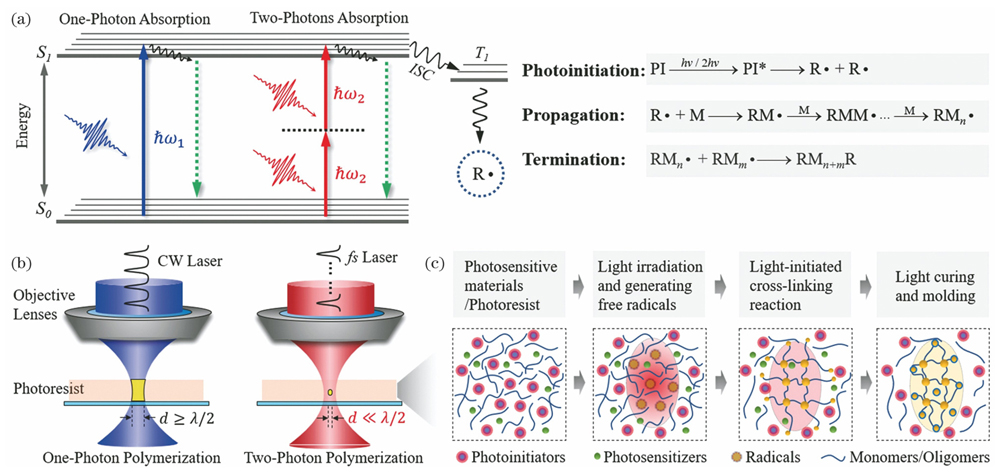
    Fig. 1. Principle of micro-nano 3D printing based on one/two-photon polymerization. (a) Schematic of one/two-photon absorption energy level transitions and polymerization process, where represents photon energy, S0 represents ground state, S1 represents excited singlet state, T1 represents triplet state, and ISC represents intersystem crossing; (b) schematic of feature scales of one/two-photon polymerization, where d represents the minimum print feature scale; (c) schematic of one/two-photon polymerization and crosslinking process of photoresist
    A typical laser direct writing micro-nano 3D printing system. (a) Schematic of optical path; (b) schematic of a parallel laser beam generation scheme
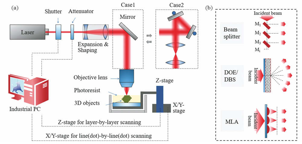
    Fig. 2. A typical laser direct writing micro-nano 3D printing system. (a) Schematic of optical path; (b) schematic of a parallel laser beam generation scheme
    A typical laser projection micro-nano 3D printing system. (a) Schematic of optical path; (b) schematic of a“digital mask”generation scheme for surface projection
    Fig. 3. A typical laser projection micro-nano 3D printing system. (a) Schematic of optical path; (b) schematic of a“digital mask”generation scheme for surface projection
    Micro-nano 3D printing based on one-photon polymerization and resolution. (a) 3D printing equipment based on stereolithography and the first 3D printed object[95]; (b) microgear structure and 1.2 μm feature size structure[96]; (c) microrotor structure and nanowire with linewidth of 0.43 μm[97-98]; (d) woodpile structure and nanowire with linewidth of 85 nm[99]; (e) spiral photonic crystal structure and nanodots with diameter of 190 nm[100]; (f) woodpile photonic crystals, cage structure and nanodot array with diameter of 85 nm[101]; (g) spiral photonic crystals and nanowire with linewidth of 0.6 μm[102]; (h) high-precision projection lithography system and 180 nm feature size structure[103]
    Fig. 4. Micro-nano 3D printing based on one-photon polymerization and resolution. (a) 3D printing equipment based on stereolithography and the first 3D printed object[95]; (b) microgear structure and 1.2 μm feature size structure[96]; (c) microrotor structure and nanowire with linewidth of 0.43 μm[97-98]; (d) woodpile structure and nanowire with linewidth of 85 nm[99]; (e) spiral photonic crystal structure and nanodots with diameter of 190 nm[100]; (f) woodpile photonic crystals, cage structure and nanodot array with diameter of 85 nm[101]; (g) spiral photonic crystals and nanowire with linewidth of 0.6 μm[102]; (h) high-precision projection lithography system and 180 nm feature size structure[103]
    Micro-nano 3D printing based on two-photon polymerization and resolution. (a)(c) Schematic of two-photon polymerization printing and“nano cattle”prepared by the technology[64]; (d)(f) two-photon polymerization area, voxel morphology and the structure with 120 nm feature size[64,77]; (g)(j) nanowires with the minimum linewidth of 100, 80, 50, and 35 nm on the glass substrate[107-111]; (k)(m) dangling nanowires with the minimum linewidth of 30, 23, and 7 nm[105,112-113]
    Fig. 5. Micro-nano 3D printing based on two-photon polymerization and resolution. (a)(c) Schematic of two-photon polymerization printing and“nano cattle”prepared by the technology[64]; (d)(f) two-photon polymerization area, voxel morphology and the structure with 120 nm feature size[64,77]; (g)(j) nanowires with the minimum linewidth of 100, 80, 50, and 35 nm on the glass substrate[107-111]; (k)(m) dangling nanowires with the minimum linewidth of 30, 23, and 7 nm[105,112-113]
    Super-resolution imaging technology-assisted two-photon polymerization micro-nano 3D printing. (a)(c) Schematic of STED two-photon printing and the minimum longitudinal size of 40 nm[116]; (d)(f) nanowires fabricated by STED single-photon lithography with the minimum size of 64 nm and 35 nm[117-118]; (g)(h) nanowires fabricated by STED two-photon lithography with the minimum size of 54 nm and 9 nm[124]; (i)(j) schematic of 4Pi multiphoton polymerization and nanowires fabricated by the technique with the minimum axial size of 150 nm[127]
    Fig. 6. Super-resolution imaging technology-assisted two-photon polymerization micro-nano 3D printing. (a)(c) Schematic of STED two-photon printing and the minimum longitudinal size of 40 nm[116]; (d)(f) nanowires fabricated by STED single-photon lithography with the minimum size of 64 nm and 35 nm[117-118]; (g)(h) nanowires fabricated by STED two-photon lithography with the minimum size of 54 nm and 9 nm[124]; (i)(j) schematic of 4Pi multiphoton polymerization and nanowires fabricated by the technique with the minimum axial size of 150 nm[127]
    Multifocus parallel printing and microstructure array. (a)(b) The letter“N”and microspring array fabricated by parallel MLA-TPP[129]; (c)(d) microgear and micron“cattle”array fabricated by parallel DOE-TPP[131]; (e)(h) multifocus TPP system and prepared three-dimensional mechanical metamaterial by this system[133]
    Fig. 7. Multifocus parallel printing and microstructure array. (a)(b) The letter“N”and microspring array fabricated by parallel MLA-TPP[129]; (c)(d) microgear and micron“cattle”array fabricated by parallel DOE-TPP[131]; (e)(h) multifocus TPP system and prepared three-dimensional mechanical metamaterial by this system[133]
    Holographic multifocal printing and microstructure arrays. (a) Dynamic holographic TPP method and fabricated 3D microtube by this method[138]; (b) multi-dodecahedron microstructure exposed by 5 foci of holographic TPP[139]; (c) SLM holographic multifocus 3D TPP method and fabricated 3-layer and 6-layer 3D structures by the method with holographic 20-focus[140]; (d) DMD holographic multifocus 3D TPP method and printed high-resolution“bridge”structure by the method, and woodpile structures printed by single-focus, double-foci, and three-foci TPP generated with the binary holography[146]
    Fig. 8. Holographic multifocal printing and microstructure arrays. (a) Dynamic holographic TPP method and fabricated 3D microtube by this method[138]; (b) multi-dodecahedron microstructure exposed by 5 foci of holographic TPP[139]; (c) SLM holographic multifocus 3D TPP method and fabricated 3-layer and 6-layer 3D structures by the method with holographic 20-focus[140]; (d) DMD holographic multifocus 3D TPP method and printed high-resolution“bridge”structure by the method, and woodpile structures printed by single-focus, double-foci, and three-foci TPP generated with the binary holography[146]
    Fast surface projection 3D printing. (a) 3D printing method for continuous liquid interface production and prepared“Eiffel Tower”model by the method[48]; (b) large-area fast printing based on mobile-liquid interface and prepared mechanical metamaterials by the method[150]; (c) rapid continuous stereolithography based on STED and printed hollow structures by the method[151]; (d) dynamic conformal 3D printing method and prepared real-time bending conversion model of“Eiffel Tower”by the method[152]
    Fig. 9. Fast surface projection 3D printing. (a) 3D printing method for continuous liquid interface production and prepared“Eiffel Tower”model by the method[48]; (b) large-area fast printing based on mobile-liquid interface and prepared mechanical metamaterials by the method[150]; (c) rapid continuous stereolithography based on STED and printed hollow structures by the method[151]; (d) dynamic conformal 3D printing method and prepared real-time bending conversion model of“Eiffel Tower”by the method[152]
    DMD surface projection stereolithography. (a) Femtosecond projection TPL technology based on DMD and prepared millimeter-scale 3D structure with submicrometer features, and micro-nano bridge structure by the technology[49]; (b) DMD projection multi-photon 3D printing with spatiotemporal focusing technology and prepared suspension line structures, micro-nano suspended lines structures, and macro-metamaterial structures by the technology[50]; (c) femtosecond projection nanolithography technology based on DMD and prepared nanowires and nanodots structures, and cross-scale micro-nano structures by the technology[158]
    Fig. 10. DMD surface projection stereolithography. (a) Femtosecond projection TPL technology based on DMD and prepared millimeter-scale 3D structure with submicrometer features, and micro-nano bridge structure by the technology[49]; (b) DMD projection multi-photon 3D printing with spatiotemporal focusing technology and prepared suspension line structures, micro-nano suspended lines structures, and macro-metamaterial structures by the technology[50]; (c) femtosecond projection nanolithography technology based on DMD and prepared nanowires and nanodots structures, and cross-scale micro-nano structures by the technology[158]
    Volume projection stereolithography. (a)(b) One-step volumetric additive manufacturing and printed arbitrary 3D structures by the method[159]; (c)(d) dual-color light induced-suppressed photopolymerization volumetric 3D printing and printed 3D objects by the method[160]; (e)(g) dual-color xolography volumetric 3D printing and prepared spherical cage with free-floating ball and anatomical model structure by the method[161]
    Fig. 11. Volume projection stereolithography. (a)(b) One-step volumetric additive manufacturing and printed arbitrary 3D structures by the method[159]; (c)(d) dual-color light induced-suppressed photopolymerization volumetric 3D printing and printed 3D objects by the method[160]; (e)(g) dual-color xolography volumetric 3D printing and prepared spherical cage with free-floating ball and anatomical model structure by the method[161]
    Volume projection stereolithography based on tomographic reconstruction. (a)(b) Printing principle and equipment of volume 3D printing based on tomographic reconstruction[163]; (c)(d) preparation process and 3D geometric structures[163]; (e)(f) high-resolution tomographic 3D printing with integrated feedback system, prepared high-fidelity structures in the modes with and without feedback[164]
    Fig. 12. Volume projection stereolithography based on tomographic reconstruction. (a)(b) Printing principle and equipment of volume 3D printing based on tomographic reconstruction[163]; (c)(d) preparation process and 3D geometric structures[163]; (e)(f) high-resolution tomographic 3D printing with integrated feedback system, prepared high-fidelity structures in the modes with and without feedback[164]
    Comparison of process performance of different types of photopolymerization micro-nano 3D printing/lithography technologies
    Fig. 13. Comparison of process performance of different types of photopolymerization micro-nano 3D printing/lithography technologies
    Minimum line spacing structure prepared by micro-nano 3D printing. (a) Diffraction-limited light intensity (red) of line array for parallel exposures, where the incident wavelength is 800 nm and NA is 1.4[120]; (b) two adjacent lines fabricated by STED lithography with different line spacing values[124]; (c) two adjacent lines fabricated by STED lithography with the different intensities of inhibition laser beam[125]; (d) two suspension lines fabricated by TPP lithography with the different line spacing values[105]
    Fig. 14. Minimum line spacing structure prepared by micro-nano 3D printing. (a) Diffraction-limited light intensity (red) of line array for parallel exposures, where the incident wavelength is 800 nm and NA is 1.4[120]; (b) two adjacent lines fabricated by STED lithography with different line spacing values[124]; (c) two adjacent lines fabricated by STED lithography with the different intensities of inhibition laser beam[125]; (d) two suspension lines fabricated by TPP lithography with the different line spacing values[105]
    Large-area splicing structures prepared by micro-nano 3D printing. (a)(b) Macroscopic foam disk (1.5 mm in diameter, 100150 μm in thickness) constructed from individual layers consisting of stitched 100 μm×100 μm×16 μm logpile blocks[177]; (c)(d) 3D gyroid structures printed with scanners only and using continuous writing via synchronized linear stages and galvo-scanners[178]; (e)(f) Yggdrasil structure printed with high-magnification (63×, NA of 1.4) and low-magnification (20×, NA of 0.5) microscope objectives, respectively, and the stitching scheme used for low-magnification objective[179]; (g)(h) printed structures using only galvanometric scanners, and continuous scanning via synchronization of both linear translation stages and galvanometric scanners[166]; (i) a mesoscale butterfly created by continuous scanning via synchronization of both linear translation stages and galvanometric scanners[166]
    Fig. 15. Large-area splicing structures prepared by micro-nano 3D printing. (a)(b) Macroscopic foam disk (1.5 mm in diameter, 100150 μm in thickness) constructed from individual layers consisting of stitched 100 μm×100 μm×16 μm logpile blocks[177]; (c)(d) 3D gyroid structures printed with scanners only and using continuous writing via synchronized linear stages and galvo-scanners[178]; (e)(f) Yggdrasil structure printed with high-magnification (63×, NA of 1.4) and low-magnification (20×, NA of 0.5) microscope objectives, respectively, and the stitching scheme used for low-magnification objective[179]; (g)(h) printed structures using only galvanometric scanners, and continuous scanning via synchronization of both linear translation stages and galvanometric scanners[166]; (i) a mesoscale butterfly created by continuous scanning via synchronization of both linear translation stages and galvanometric scanners[166]
    Low-cost micro-nano 3D printing systems and microstructures. (a) 3D printer using high-definition digital versatile discs (HD DVDs) optical-pickup-unit (OPU) as core optical module, laser beam of 405 nm wavelength was focused to cure photopolymer[190]; (b)(e) 3D printed nanoscale line structures with the widths of 992, 879, 769, and 385 nm, and tower structures[190]; (f) semiconductor laser diode used in two-step absorption 3D nanoprinter, operating at 405 nm wavelength[192]; (g) printed 2D line gratings[192]; (h)(l) various 3D-printed nanostructures[192]
    Fig. 16. Low-cost micro-nano 3D printing systems and microstructures. (a) 3D printer using high-definition digital versatile discs (HD DVDs) optical-pickup-unit (OPU) as core optical module, laser beam of 405 nm wavelength was focused to cure photopolymer[190]; (b)(e) 3D printed nanoscale line structures with the widths of 992, 879, 769, and 385 nm, and tower structures[190]; (f) semiconductor laser diode used in two-step absorption 3D nanoprinter, operating at 405 nm wavelength[192]; (g) printed 2D line gratings[192]; (h)(l) various 3D-printed nanostructures[192]
    Yuanyuan Zhao, Haichao Luo, Zixin Liang, Mingjie Deng, Xuanming Duan. Micro-Nano 3D Printing Based on Photopolymerization and Its Development Status and Trends[J]. Chinese Journal of Lasers, 2022, 49(10): 1002703
    Download Citation