• Chinese Optics Letters
  • Vol. 20, Issue 3, 031406 (2022)
Yuying Wang1, Lijing Zhong2, Zhi Chen2、*, Dezhi Tan2、**, Zaijin Fang3, Yi Yang4, Shengzhi Sun5, Lüyun Yang6, and Jianrong Qiu1、4
Author Affiliations
  • 1Ningbo Femto & Nano Laser Technology Co., Ltd., Ningbo 315000, China
  • 2Zhejiang Lab, Hangzhou 311100, China
  • 3Guangdong Provincial Key Laboratory of Optical Fiber Sensing and Communications, Institute of Photonics Technology, Jinan University, Guangzhou 511443, China
  • 4State Key Laboratory of Modern Optical Instrumentation, College of Optical Science and Engineering, Zhejiang University, Hangzhou 310027, China
  • 5Laboratory of Infrared Materials and Devices, The Research Institute of Advanced Technologies, Ningbo University, Ningbo 315211, China
  • 6Wuhan National Laboratory for Optoelectronics, Huazhong University of Science and Technology, Wuhan 430074, China
  • show less
    DOI: 10.3788/COL202220.031406 Cite this Article Set citation alerts
    Yuying Wang, Lijing Zhong, Zhi Chen, Dezhi Tan, Zaijin Fang, Yi Yang, Shengzhi Sun, Lüyun Yang, Jianrong Qiu. Photonic lattice-like waveguides in glass directly written by femtosecond laser for on-chip mode conversion[J]. Chinese Optics Letters, 2022, 20(3): 031406 Copy Citation Text show less
    Design scheme and simulation of PLLW. (a) Schematic diagram of PLLW. Insert: ring-shape output. (b) Simulated mode field of input side. (c) Simulated mode field of output side.
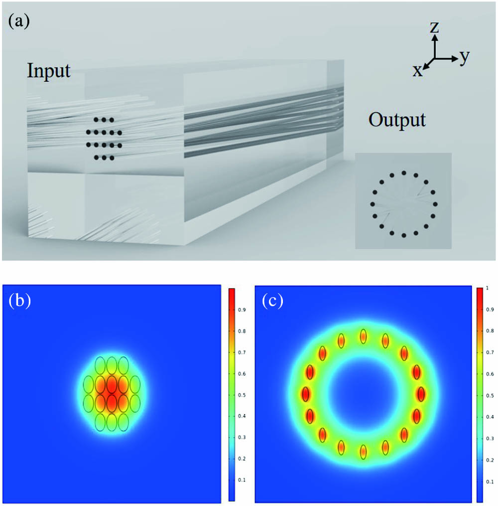
    Fig. 1. Design scheme and simulation of PLLW. (a) Schematic diagram of PLLW. Insert: ring-shape output. (b) Simulated mode field of input side. (c) Simulated mode field of output side.
    (a) Processing parameter window of the FLDW single track in PG. Top-view of different regional tracks consistent with window (b) I, (c) II, and (d) III in (a), respectively. All of the tracks are written with depths of 200 µm.
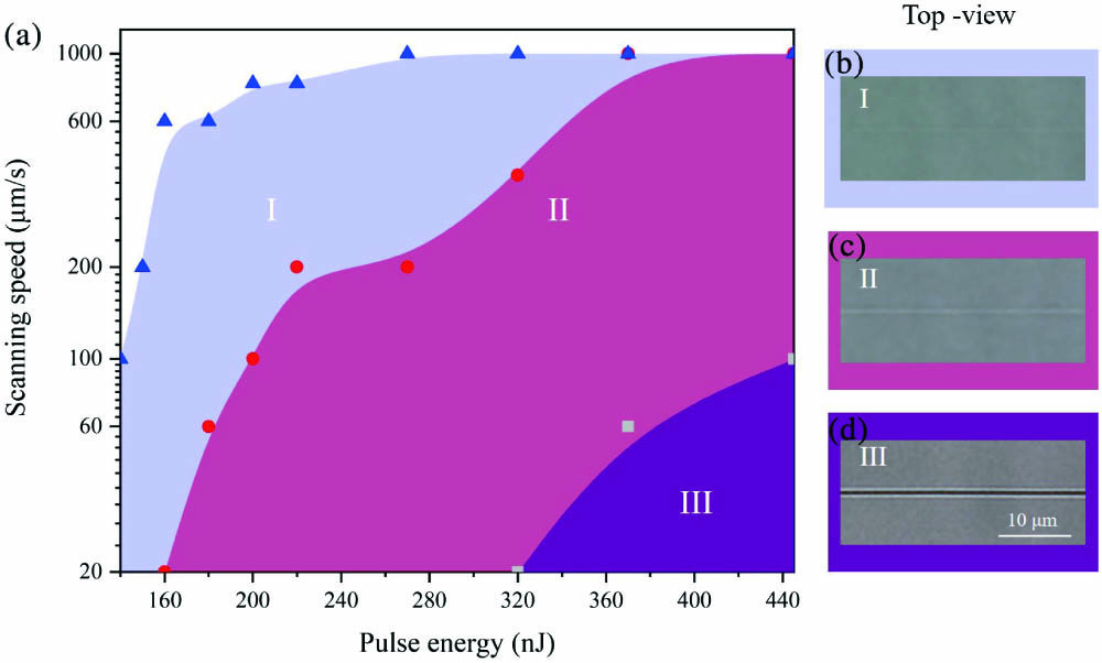
    Fig. 2. (a) Processing parameter window of the FLDW single track in PG. Top-view of different regional tracks consistent with window (b) I, (c) II, and (d) III in (a), respectively. All of the tracks are written with depths of 200 µm.
    Dependence of the width and length of densified tracks on FLDW depth. Inserts: microscopic cross-section images of tracks in different depths. Scale bar: 1 µm. All of the tracks are written with scanning speed of 40 µm/s in PG.
    Fig. 3. Dependence of the width and length of densified tracks on FLDW depth. Inserts: microscopic cross-section images of tracks in different depths. Scale bar: 1 µm. All of the tracks are written with scanning speed of 40 µm/s in PG.
    Microscopic cross-section images of the PLLW (a) input and (b) output with a ring radius of 4 µm. The PLLW is written with scanning speed of 40 µm/s and pulse energy of 175 nJ. Microscopic cross-section images of the PLLW (c) input and (d) output with a ring radius of 8 µm. The PLLW is written with scanning speed of 40 µm/s and pulse energy of 165 nJ. The near-field distributions of PLLWs with a ring radius of (e) 4 µm and (f) 8 µm. Inserts: mode images of input and output sides.
    Fig. 4. Microscopic cross-section images of the PLLW (a) input and (b) output with a ring radius of 4 µm. The PLLW is written with scanning speed of 40 µm/s and pulse energy of 175 nJ. Microscopic cross-section images of the PLLW (c) input and (d) output with a ring radius of 8 µm. The PLLW is written with scanning speed of 40 µm/s and pulse energy of 165 nJ. The near-field distributions of PLLWs with a ring radius of (e) 4 µm and (f) 8 µm. Inserts: mode images of input and output sides.
    Yuying Wang, Lijing Zhong, Zhi Chen, Dezhi Tan, Zaijin Fang, Yi Yang, Shengzhi Sun, Lüyun Yang, Jianrong Qiu. Photonic lattice-like waveguides in glass directly written by femtosecond laser for on-chip mode conversion[J]. Chinese Optics Letters, 2022, 20(3): 031406
    Download Citation