
Yuying Wang, Lijing Zhong, Zhi Chen, Dezhi Tan, Zaijin Fang, Yi Yang, Shengzhi Sun, Lüyun Yang, Jianrong Qiu, "Photonic lattice-like waveguides in glass directly written by femtosecond laser for on-chip mode conversion," Chin. Opt. Lett. 20, 031406 (2022)
- Chinese Optics Letters
- Vol. 20, Issue 3, 031406 (2022)
Abstract
1. Introduction
Femtosecond laser direct writing (FLDW) has shown great potential for manufacturing diverse components of complete on-chip integrated photonics, including light source, modulator, light computation, and detection[
As is known, local modification triggered by nonlinear absorption of femtosecond pulses in a well-confined focal region is very complicated, including electronic excitation, relaxation, and thermal effect. Particularly, due to the influence of thermal diffusion or accumulation, the final size of the modified region is routinely quite large, and its morphology is usually non-regular/non-symmetrical[
Herein, we propose a new concept to create 3D waveguides in glass called the photonic lattice-like waveguide (PLLW). Guiding is supported by total internal reflection, which is achieved by an effective refractive index difference between a central photonic lattice-like core region and the surrounding pristine glass, and does not rely on the photonic bandgap effect. Interestingly, the PLLW is based on a sub-micro-sized densified track arrays imposing a positive refractive index change of the waveguide’s core, which is completely distinct from the cases in the past[
Sign up for Chinese Optics Letters TOC. Get the latest issue of Chinese Optics Letters delivered right to you!Sign up now
2. Design and Numerical Simulation
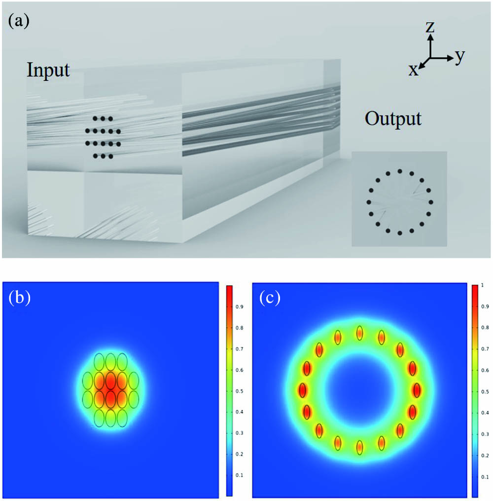
A PLLW created by tightly distributed tracks with a hexagonal-shape input and a ring-shape output [Fig. 1(a) and insert] is implemented by designing each writing path. The width and length size of a single track is designed at
![]()
Figure 1.Design scheme and simulation of PLLW. (a) Schematic diagram of PLLW. Insert: ring-shape output. (b) Simulated mode field of input side. (c) Simulated mode field of output side.
To understand the difference of guiding modes of PLLW at the input and output, a finite element method is used to study the mode fields of the photonic lattice structure. The refractive index difference between densified tracks and pristine material is set to
3. Femtosecond Laser Processing Experiments
To experimentally verify the feasibility of our theoretical design, a nanoporous silica glass (PG) with averaged pore size of
In our experiment, the tracks are fabricated with a chirped pulse amplified femtosecond Yb∶KGd(WO4)20 (Yb:KGW) laser source (Pharos, Light Conversion) that delivers 226 fs pulses with 200 kHz repetition rate, and the central wavelength is 1030 nm. The scanning speed and depth of the FLDW tracks and PLLW are adjusted by a computer-controlled 3D nano-translation stage (SmartAct). The laser beam is linearly polarized and focused by a
The processing parameter window of the FLDW single track in the PG is shown in Fig. 2(a). Region I represents the partial densification tracks that can be inscribed at low pulse energy and/or high scanning speed, as shown in Fig. 2(b) (typical top view). In this region, the writing trace exhibits small positive refractive index change. The transition from partial densification to complete densification occurs in region II, and its typical example is shown in Fig. 2(c), where the tracks appear as a bright line, indicating a greater increase in refractive index compared to region I. As femtosecond laser pulse energy increases and/or the scanning speed decreases, due to enhanced energy accumulation in the modified region, voids appear in the center of damaged tracks with negative refractive index change [see typical top-view shown in Fig. 2(d)].
![]()
Figure 2.(a) Processing parameter window of the FLDW single track in PG. Top-view of different regional tracks consistent with window (b) I, (c) II, and (d) III in (a), respectively. All of the tracks are written with depths of 200 µm.
Since the refractive index change in region II is considerably positive, and no voids appear, region II is deliberately distinguished and selected to process PLLW. The laser scanning speed of 40 µm/s is selected to verify the effect of direct-writing depths on the track size. With the increase of direct-writing depth, the pulse energy is gradually increased (from 55 to 185 nJ) to ensure that the refractive index changes of tracks are basically the same. As shown in Fig. 3, the length of tracks changes from 1.67 to 3.50 µm as the direct-writing depth increases from 10 to 200 µm due to influence of surface aberration. On the contrary, the width of the tracks is basically constant and less than 1 µm as the direct-writing depth increases, and the minimum width of densified track is 0.62 µm. By calculating the diffraction limit of the objective with
![]()
Figure 3.Dependence of the width and length of densified tracks on FLDW depth. Inserts: microscopic cross-section images of tracks in different depths. Scale bar: 1 µm. All of the tracks are written with scanning speed of 40 µm/s in PG.
4. Results and Discussion
Based on the study on densification parameters of tracks and design scheme of PLLW, two waveguides are fabricated by FLDW in PG, namely, same hexagonal-shape input with width of 4 µm and ring-shape output with two different radii of 4 µm and 8 µm. In order to ensure good distribution of densified tracks and the same shape as the hexagon, the direct-writing depth is increased from 100 µm at the input to 170 µm at the output, and scanning speed is 40 µm/s.
The hexagonal-shape inputs of the two PLLWs have the same width and length of 4 µm, as shown in Figs. 4(a) and 4(c). Due to the influence of surface aberration, the ring becomes ellipse like, as shown in Figs. 4(b) and 4(d). The major and minor axes of the ellipse with the designed radii of 4 and 8 µm are measured as
![]()
Figure 4.Microscopic cross-section images of the PLLW (a) input and (b) output with a ring radius of 4 µm. The PLLW is written with scanning speed of 40 µm/s and pulse energy of 175 nJ. Microscopic cross-section images of the PLLW (c) input and (d) output with a ring radius of 8 µm. The PLLW is written with scanning speed of 40 µm/s and pulse energy of 165 nJ. The near-field distributions of PLLWs with a ring radius of (e) 4 µm and (f) 8 µm. Inserts: mode images of input and output sides.
The demonstration of the PLLW for mode conversion is governed in terms of near-field distribution and insertion losses. A typical end-coupling system is employed with a 976 nm single-mode fiber laser (MChlight) with core diameter of 4 µm. The near-field intensity distribution is collected by a
To evaluate the mode conversion efficiency, the insertion losses of the waveguide are estimated by measuring the input and output power directly. As the writing pulse energy changes from 115 to 185 nJ, the insertion losses measured increase from 1.65 and 3.20 dB. Fascinatingly, the insertion loss of 1.65 dB is quite low for FLDW waveguides in glass. The reason for such low insertion loss is that the hexagonal-shape input of the PLLW is centrosymmetric and nearly circular, which has been proved to have high coupling efficiency with the fiber used for coupling[
5. Conclusion
In conclusion, PLLW with a hexagonal-shape input and a ring-shape output is proposed, as a new concept of waveguide. The PLLW consists of 16 sub-micron sized densified tracks with positive refractive index change by FLDW in glass. The sub-micron tracks with minimum width of 0.62 µm have successfully been fabricated. Finally, a mode conversion application of PLLW with different shapes of input and output is demonstrated, which transforms the mode field from a Gaussian mode to a doughnut-like one with a high conversion efficiency indicated by the insertion loss as low as 1.65 dB at 976 nm, and its mode size can be controlled by tailoring the output ring shape. This work provides a new freedom for design and fabrication of waveguides with sub-micron resolution, which will contribute to development of on-chip all-optical integrated photonic devices in future.
References
[1] G. Corrielli, A. Crespi, R. Osellame. Femtosecond laser micromachining for integrated quantum photonics. Nanophotonics, 10, 3789(2021).
[2] Y. Chen, J. Gao, Z. Jiao, K. Sun, W. Shen, L. Qiao, H. Tang, X. Lin, X. Jin. Mapping twisted light into and out of a photonic chip. Phys. Rev. Lett., 121, 233602(2018).
[3] A. Seri, G. Corrielli, D. Lago-Rivera, A. Lenhard, H. de Riedmatten, R. Osellame, M. Mazzera. Laser-written integrated platform for quantum storage of heralded single photons. Optica, 5, 934(2018).
[4] F. Shen, X. Shu, K. Zhou, H. Jiang, H. Xia, K. Xie, L. Zhang. Compact vector twist sensor using a small period long period fiber grating inscribed with femtosecond laser. Chin. Opt. Lett., 19, 090601(2021).
[5] A. El Hassan, F. K. Kunst, A. Moritz, G. Andler, E. J. Bergholtz, M. Bourennane. Corner states of light in photonic waveguides. Nat. Photonics, 13, 697(2019).
[6] D. Tan, B. Zhang, J. Qiu. Ultrafast laser direct writing in glass: thermal accumulation engineering and applications. Laser Photonics Rev., 15, 2000455(2021).
[7] D. Tan, Z. Wang, B. Xu, J. Qiu. Photonic circuits written by femtosecond laser in glass: improved fabrication and recent progress in photonic devices. Adv. Photonics, 3, 024002(2021).
[8] S. M. Eaton, M. L. Ng, R. Osellame, P. R. Herman. High refractive index contrast in fused silica waveguides by tightly focused, high-repetition rate femtosecond laser. J. Non-Cryst. Solids., 357, 2387(2011).
[9] F. Yu, L. Wang, Y. Chen, Q. Chen, Z. Tian, X. Ren, H. Sun. Polarization independent quantum devices with ultra-low birefringence glass waveguides. J. Lightwave Technol., 39, 1451(2021).
[10] Z. Li, X. Li, F. Yu, Q. Chen, Z. Tian, H. Sun. Circular cross section waveguides processed by multi-foci-shaped femtosecond pulses. Opt. Lett., 46, 520(2021).
[11] G. Corrielli, A. Crespi, R. Geremia, R. Ramponi, L. Sansoni, A. Santinelli, P. Mataloni, F. Sciarrino, R. Osellame. Rotated waveplates in integrated waveguide optics. Nat. Commun., 5, 4249(2014).
[12] D. Tan, X. Sun, Q. Wang, P. Zhou, Y. Liao, J. Qiu. Fabricating low loss waveguides over a large depth in glass by temperature gradient assisted femtosecond laser writing. Opt. Lett., 45, 3941(2020).
[13] Y. Jia, S. Wang, F. Chen. Femtosecond laser direct writing of flexibly configured waveguide geometries in optical crystals: fabrication and application. Opto-Electron. Adv., 3, 190042(2020).
[14] G.-L. Roth, S. Kefer, S. Hessler, C. Esen, R. Hellmann. Polymer photonic crystal waveguides generated by femtosecond laser. Laser Photonics Rev., 15, 2100215(2021).
[15] W. Nie, R. He, C. Cheng, U. Rocha, J. Rodriguez Vazquez de Aldana, D. Jaque, F. Chen. Optical lattice-like cladding waveguides by direct laser writing: fabrication, luminescence, and lasing. Opt. Lett., 41, 2169(2016).
[16] Y. Jia, C. Cheng, J. R. Vázquez de Aldana, F. Chen. Three-dimensional waveguide splitters inscribed in Nd:YAG by femtosecond laser writing: realization and laser emission. J. Lightwave Technol., 34, 1328(2016).
[17] G. R. Castillo, L. Labrador-Paez, F. Chen, S. Camacho-Lopez, J. R. V. de Aldana. Depressed-cladding 3-D waveguide arrays fabricated with femtosecond laser pulses. J. Lightwave Technol., 35, 2520(2017).
[18] B. Zhang, L. Wang, F. Chen. Recent advances in femtosecond laser processing of LiNbO3 crystals for photonic applications. Laser Photonics Rev., 14, 1900407(2020).
[19] R. Li, L. Sun, Y. Cai, Y. Ren, H. Liu, M. D. Mackenzie, A. K. Kar. Near-infrared lasing and tunable upconversion from femtosecond laser inscribed Nd, Gd:CaF2 waveguides. Chin. Opt. Lett., 19, 081301(2021).
[20] L. Zhong, R. A. Zakoldaev, M. M. Sergeev, V. P. Veiko, Z. Li. Porous glass density tailoring by femtosecond laser pulses. Opt. Quant. Electron., 52, 49(2020).
[21] Y. Chu, Y. Yang, L. Liao, Y. Liu, Y. Ma, X. Hu, Y. Wang, Y. Xing, J. Peng, H. Li, N. Dai, J. Li, L. Yang. 3D nanoporous silica rods for extra-large-core high-power fiber lasers. ACS Photonics, 5, 4014(2018).
[22] L. Yang, N. Dai, Z. Liu, Z. Jiang, J. Peng, H. Li, J. Li, M. Yamashita, T. Akai. Tailoring of clusters of active ions in sintered nanoporous silica glass for white light luminescence. J. Mater. Chem., 21, 6274(2011).
[23] Z. Liu, N. Dai, H. Luan, Y. Sheng, J. Peng, Z. Jiang, H. Li, L. Yang, J. Li. Enhanced green luminescence in Ce-Tb-Ca codoped sintered porous glass. Opt. Express, 18, 21138(2010).
[24] V. P. Veiko, S. I. Kudryashov, M. M. Sergeev, R. A. Zakoldaev, P. A. Danilov, A. A. Ionin, T. V. Antropova, I. N. Anfimova. Femtosecond laser-induced stress-free ultra-densification inside porous glass. Laser Phys. Lett., 13, 055901(2016).
[25] T. E. Itina, R. A. Zakoldaev, M. M. Sergeev, H. Ma, S. I. Kudryashov, O. S. Medvedev, V. P. Veiko. Ultra-short laser-induced high aspect ratio densification in porous glass. Opt. Mater. Express, 9, 4379(2019).
[26] V. P. Veiko, R. A. Zakoldaev, M. M. Sergeev, P. A. Danilov, S. I. Kudryashov, G. K. Kostiuk, A. N. Sivers, A. A. Ionin, T. V. Antropova, O. S. Medvedev. Direct laser writing of barriers with controllable permeability in porous glass. Opt. Express, 26, 28150(2018).
[27] L. Zhong, R. A. Zakoldaev, M. M. Sergeev, V. P. Veiko. Fluorescent bulk waveguide sensor in porous glass: concept, fabrication, and testing. Nanomaterials, 10, 2169(2020).
[28] B. Sun, F. Morozko, P. S. Salter, S. Moser, Z. Pong, R. B. Patel, I. A. Walmsley, A. Hazan, N. Barré, A. Jesacher, J. Fells, A. Katiyi, A. Novitsky, A. Karabchevsky, M. J. Booth. On-chip beam rotators, polarizers and adiabatic mode converters through low-loss waveguides with variable cross-sections(2021).
[29] H. Norman, H. Weber. Laser Resonators and Beam Propagation: Fundamentals, Advanced Concepts and Applications(2005).
[30] Y. Xiao, X. Tang, C. Wan, Y. Qin, H. Peng, C. Hu, B. Qin. Laguerre–Gaussian mode expansion for arbitrary optical fields using a subspace projection method. Opt. Lett., 44, 1615(2019).


Set citation alerts for the article
Please enter your email address

© Copyright 2018-2021 | Chinese Laser Press. All Rights Reserved 沪ICP备15018463号-20