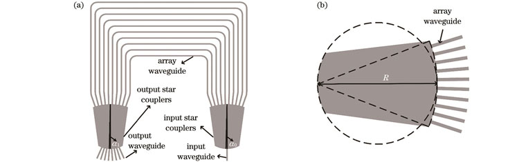
With the rapid development of large traffic network, the demand for data exchange rates is increasing daily. Wavelength-division multiplexing (WDM) has garnered considerable attention in optical communication networks owing to its high communication speed, transparent signal transmission, efficient expansion of transmission capacity, and low cost. Dense wavelength division multiplexing (DWDM) is a crucial component of the optical communication field because it increases the capacity of communication systems and satisfies the public demand for greater communication bandwidth. Arrayed waveguide gratings (AWG) have low crosstalk, low insertion loss, high uniformity, high reliability, and a compact structure. Therefore, they have become the most commonly employed technical solution for DWDM. AWGs have been demonstrated in low-refractive-index-contrast materials, such as InP, silica, and polymers. The refractive-index contrast of the core and cladding of these materials is low; therefore, the device size and bending loss are large, which is unfavorable for the development of highly integrated DWDM systems. Owing to the high refractive-index contrast, a silicon waveguide arrayed waveguide grating can be made extremely compact, allowing for low-cost and high-volume manufacturing owing to its complementary metal-oxide semiconductor (CMOS)-compatible processing. Many arrayed waveguide gratings using silicon waveguides have been proposed. However, they still need to be further reduced in size to increase integration, and the uniformity of each output channel needs to be improved.
A compact, highly uniform silicon-arrayed waveguide grating is studied. First, the arrayed waveguide grating is theoretically analyzed to understand its design scheme and performance parameters. Subsequently, the waveguide bending loss and effective index versus the silicon waveguide bending radius are simulated (Fig. 3). With a gradual decrease in the bending radius, the bending loss and effective index first decrease and then stabilize. When the bending radius is between 2.5 μm and 5.0 μm, the bending loss exceeds 1.29 dB, and the effective index of the silicon waveguide is greatly affected by the bending radius. When the bending radius exceeds 15 μm, the bending loss is less than 0.028 dB. The silicon waveguide's bending loss is negligible, and the effective index of the waveguide is stable at 2.449. According to the comprehensive consideration of device performance, the bending radius is 15 μm. Finally, according to the basic principles of arrayed waveguide gratings and the related parameters of silicon waveguides, the main structural parameters of the compact and highly uniform silicon waveguide arrayed waveguide gratings are determined (Table 1). Subsequently, a compact silicon-arrayed waveguide grating is fabricated on a silicon on insulator (SOI) platform. Finally, a test system is built to obtain the spectral characteristics of the silicon-arrayed waveguide grating chip, and each parameter is presented.
In this study, a silicon-arrayed waveguide grating chip is prepared and tested. The chip realizes 8-channel 200-GHz WDM, and its structure size is only 294 μm×190 μm. The performance of each parameter is calculated according to the relevant definitions. The minimum insertion loss value is 19.6 dB, crosstalk is -15 dB, nonuniformity of the channel is 0.87 dB, and 3 dB bandwidth is 1.06 nm. The insertion loss during the testing process mainly originates from the coupling loss of the test system and the on-chip loss of the arrayed waveguide grating. The coupling loss is approximately 10 dB, and the on-chip loss of the arrayed waveguide grating is 9.6 dB. The device adopts silicon-on-insulator technology compatible with the CMOS process; therefore, its mass and low-cost production can be realized. In addition, the device has a compact structure and high uniformity.
Based on a silicon-on-insulator material platform, a compact highly uniform silicon waveguide-arrayed grating with eight output channels and a channel spacing of 200 GHz is designed and fabricated. The effects of the bending radius of the silicon waveguide on the bending loss and effective refractive index of the silicon-on-insulator platform are analyzed. The test results show that the insertion loss of the device is 19.6 dB, the crosstalk is -15 dB, the nonuniformity is 0.87 dB, the 3 dB bandwidth is 1.06 nm, and the structure size is only 294 μm×190 μm. The chip can be produced using a CMOS process, which enables the production of arrayed waveguide gratings in large quantities at low cost. This is crucial for the development of integrated WDM networks.