• Photonics Research
  • Vol. 8, Issue 1, 91 (2020)
Zhipeng Sun1、2, Mingming Jiang1、3、*, Wangqi Mao3, Caixia Kan3, Chongxin Shan1、4、5, and Dezhen Shen1、6
Author Affiliations
  • 1State Key Laboratory of Luminescence and Applications, Changchun Institute of Optics, Fine Mechanics and Physics, Chinese Academy of Sciences, Changchun 130033, China
  • 2University of Chinese Academy of Sciences, Beijing 100049, China
  • 3College of Science, Nanjing University of Aeronautics and Astronautics, Nanjing 210016, China
  • 4School of Physics and Engineering, Zhengzhou University, Zhengzhou 450052, China
  • 5e-mail: cxshan@zzu.edu.cn
  • 6e-mail: shendz@ciomp.ac.cn
  • show less
    DOI: 10.1364/PRJ.8.000091 Cite this Article Set citation alerts
    Zhipeng Sun, Mingming Jiang, Wangqi Mao, Caixia Kan, Chongxin Shan, Dezhen Shen. Nonequilibrium hot-electron-induced wavelength-tunable incandescent-type light sources[J]. Photonics Research, 2020, 8(1): 91 Copy Citation Text show less
    EL emission characteristics from single AuNRs@ZnO:Ga MW-based incandescent-type light source (the extinction peak of Au-nanorod, 695 nm). (a) The extinction spectrum of Au nanorods, with corresponding TEM image of the Au nanorods demonstrated in the inset. (b) SEM image of single AuNRs@ZnO:Ga MW. (c) Amplified SEM image of Au nanorods deposited on the MW. (d) I−V characteristics of single ZnO:Ga MW prepared via Au nanorods decoration. (e) EL emission spectra from single ZnO:Ga MW-based fluorescent emitter. (f) EL emission spectra from single AuNRs@ZnO:Ga MW-based incandescent-type light source. (g) Optical microscopic image of the light emitting from electrically biased single ZnO:Ga MW-based fluorescent emitter (scale bar, 200 μm). (h) Optical microscopic image of the light emitting from electrically biased single AuNRs@ZnO:Ga MW-based incandescent-type light source (scale bar, 200 μm).
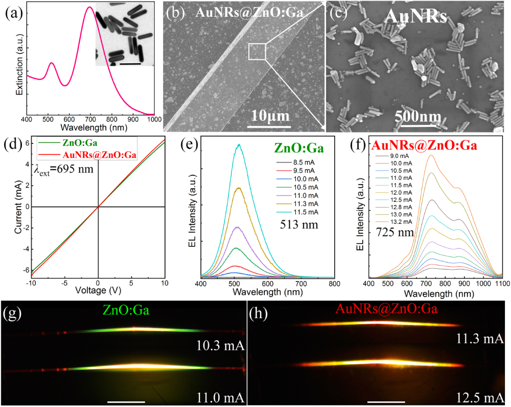
    Fig. 1. EL emission characteristics from single AuNRs@ZnO:Ga MW-based incandescent-type light source (the extinction peak of Au-nanorod, 695 nm). (a) The extinction spectrum of Au nanorods, with corresponding TEM image of the Au nanorods demonstrated in the inset. (b) SEM image of single AuNRs@ZnO:Ga MW. (c) Amplified SEM image of Au nanorods deposited on the MW. (d) IV characteristics of single ZnO:Ga MW prepared via Au nanorods decoration. (e) EL emission spectra from single ZnO:Ga MW-based fluorescent emitter. (f) EL emission spectra from single AuNRs@ZnO:Ga MW-based incandescent-type light source. (g) Optical microscopic image of the light emitting from electrically biased single ZnO:Ga MW-based fluorescent emitter (scale bar, 200 μm). (h) Optical microscopic image of the light emitting from electrically biased single AuNRs@ZnO:Ga MW-based incandescent-type light source (scale bar, 200 μm).
    (a) Optical photograph of the synthesized ZnO:Ga MWs. (b) SEM image of single ZnO:Ga MW, with perfect quadrilateral cross section displayed in the inset (scale bar, 12 μm). (c) SEM image of ZnO:Ga MW prepared with Au nanorods decoration (the spin-coating number, ×1). (d) TEM images of the Au nanorods with controlled aspect ratio. (e) The extinction spectra of Au nanorods with controlled aspect ratio. (f) PL emissions from ZnO:Ga MW prepared via Au nanorods decoration, with the controlled aspect ratios. (g) I−V behaviors of single ZnO:Ga MW prepared with Au nanorods decoration (corresponding extinction peak centered at 695 nm), with the spin-coating number ranging from 0 to 6.
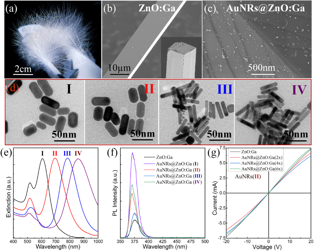
    Fig. 2. (a) Optical photograph of the synthesized ZnO:Ga MWs. (b) SEM image of single ZnO:Ga MW, with perfect quadrilateral cross section displayed in the inset (scale bar, 12 μm). (c) SEM image of ZnO:Ga MW prepared with Au nanorods decoration (the spin-coating number, ×1). (d) TEM images of the Au nanorods with controlled aspect ratio. (e) The extinction spectra of Au nanorods with controlled aspect ratio. (f) PL emissions from ZnO:Ga MW prepared via Au nanorods decoration, with the controlled aspect ratios. (g) IV behaviors of single ZnO:Ga MW prepared with Au nanorods decoration (corresponding extinction peak centered at 695 nm), with the spin-coating number ranging from 0 to 6.
    Photoconductive behavior of single AuNRs@ZnO:Ga MW [Au nanorod in Fig. 2(d) panel II, the extinction peak, 695 nm]. (a) Schematic diagram of hot carrier generation mechanisms in plasmonic Au nanorods, and then injected into ZnO:Ga MW channel under light illumination. (b) The I−V characteristics of single ZnO:Ga MW prepared with Au nanorods decoration under dark, and illumination with the excitation lasing wavelengths at 405 nm, 532 nm, and 685 nm, respectively, with the laser power density denoted as 5.0 mW/cm2. (c) The I−t characteristics with on/off switching under light illumination, with the lasing wavelengths at 405 nm, 532 nm, and 685 nm, respectively. (d) UV-vis absorption spectra of the as-synthesized ZnO:Ga MWs prepared with and without Au nanorods deposition. (e) The comparison of TRPL decays from single bare ZnO:Ga MW, and Au nanorods decorated ZnO:Ga MW. (f) Diagrammatic drawing of the physical process involving (i) photoexcitation induced electrons and (ii) plasmons induced generation, injection, or tunneling procedure of hot electrons towards the interface between Au-ZnO:Ga under light illumination.
    Fig. 3. Photoconductive behavior of single AuNRs@ZnO:Ga MW [Au nanorod in Fig. 2(d) panel II, the extinction peak, 695 nm]. (a) Schematic diagram of hot carrier generation mechanisms in plasmonic Au nanorods, and then injected into ZnO:Ga MW channel under light illumination. (b) The IV characteristics of single ZnO:Ga MW prepared with Au nanorods decoration under dark, and illumination with the excitation lasing wavelengths at 405 nm, 532 nm, and 685 nm, respectively, with the laser power density denoted as 5.0  mW/cm2. (c) The It characteristics with on/off switching under light illumination, with the lasing wavelengths at 405 nm, 532 nm, and 685 nm, respectively. (d) UV-vis absorption spectra of the as-synthesized ZnO:Ga MWs prepared with and without Au nanorods deposition. (e) The comparison of TRPL decays from single bare ZnO:Ga MW, and Au nanorods decorated ZnO:Ga MW. (f) Diagrammatic drawing of the physical process involving (i) photoexcitation induced electrons and (ii) plasmons induced generation, injection, or tunneling procedure of hot electrons towards the interface between Au-ZnO:Ga under light illumination.
    Electrical field intensity |E/E0|2 distribution of isolated Au-nanorods, with the electromagnetic wave propagating along (a) the x direction of the x–y plane (horizontal), (b) the y direction of the x–y plane (vertical), and (c) the x direction of the x–z plane (horizontal). In the simulation process, Au-nanorods with the length (50 nm) and diameter (20 nm) were adopted, accompanied with the resonant wavelength denoted as λ=695 nm, the refractive index of ZnO:Ga denoted as nZnO:Ga=2.45, and the refractive index of environmental medium air nair=1.0.
    Fig. 4. Electrical field intensity |E/E0|2 distribution of isolated Au-nanorods, with the electromagnetic wave propagating along (a) the x direction of the xy plane (horizontal), (b) the y direction of the xy plane (vertical), and (c) the x direction of the xz plane (horizontal). In the simulation process, Au-nanorods with the length (50 nm) and diameter (20 nm) were adopted, accompanied with the resonant wavelength denoted as λ=695  nm, the refractive index of ZnO:Ga denoted as nZnO:Ga=2.45, and the refractive index of environmental medium air nair=1.0.
    (a) Schematic illustration of the modulation of Au-nanorod plasmons on the incandescent-type lighting features of single ZnO:Ga MW-based fluorescent light source. (b) Normalized intensities of the EL spectrum from single bare ZnO:Ga MW-based fluorescent light source, the EL spectrum from single AuNRs@ZnO:Ga MW-based fluorescent light source, and the extinction spectrum of the deposited Au nanorods. (c) Micrographs of bright visible light emitting from an electrically driven single AuNRs@ZnO:Ga MW-based incandescent-type light source in the dark field and bright field (scale bar, 200 μm). (d) Optical microscopic images of bright visible light emitting from electrically driven single ZnO:Ga MW prepared with partial Au nanorods decoration (scale bar, 300 μm).
    Fig. 5. (a) Schematic illustration of the modulation of Au-nanorod plasmons on the incandescent-type lighting features of single ZnO:Ga MW-based fluorescent light source. (b) Normalized intensities of the EL spectrum from single bare ZnO:Ga MW-based fluorescent light source, the EL spectrum from single AuNRs@ZnO:Ga MW-based fluorescent light source, and the extinction spectrum of the deposited Au nanorods. (c) Micrographs of bright visible light emitting from an electrically driven single AuNRs@ZnO:Ga MW-based incandescent-type light source in the dark field and bright field (scale bar, 200 μm). (d) Optical microscopic images of bright visible light emitting from electrically driven single ZnO:Ga MW prepared with partial Au nanorods decoration (scale bar, 300 μm).
    Schematic diagram of the working principle of bright visible light emitting from electrically biased single AuNRs@ZnO:Ga MW-based incandescent-type light source.
    Fig. 6. Schematic diagram of the working principle of bright visible light emitting from electrically biased single AuNRs@ZnO:Ga MW-based incandescent-type light source.
    Wavelength-tunable emissions from single AuNRs@ZnO:Ga MW-based incandescent-type light source: (a) I−V characteristics of single ZnO:Ga MW via Au nanorods decoration (the extinction peak, 605 nm); (b) EL emission from single bare ZnO:Ga MW-based incandescent-type light source, with the emission wavelength centered at 527 nm; (c) EL emission from single AuNRs@ZnO:Ga MW-based incandescent-type light source, with the emission wavelength centered at 601 nm. (d) I−V characteristics of single ZnO:Ga MW prepared via Au nanorods decoration (the extinction peak, 783 nm); (e) EL emission from single bare ZnO:Ga MW-based incandescent-type light source, with the emission wavelength centered at 518 nm; (f) EL emission from the single AuNRs@ZnO:Ga MW-based incandescent-type light source, with the emission wavelength centered around 780 nm. (g) I−V characteristics of single ZnO:Ga MW via Au nanorods decoration (the extinction peak, 855 nm); (h) EL emission from the single bare ZnO:Ga MW-based incandescent-type light source, with the emission wavelength centered at 513 nm; (i) EL emission from the single AuNRs@ZnO:Ga MW-based incandescent-type light source, with the emission wavelength centered around 905 nm.
    Fig. 7. Wavelength-tunable emissions from single AuNRs@ZnO:Ga MW-based incandescent-type light source: (a) IV characteristics of single ZnO:Ga MW via Au nanorods decoration (the extinction peak, 605 nm); (b) EL emission from single bare ZnO:Ga MW-based incandescent-type light source, with the emission wavelength centered at 527 nm; (c) EL emission from single AuNRs@ZnO:Ga MW-based incandescent-type light source, with the emission wavelength centered at 601 nm. (d) IV characteristics of single ZnO:Ga MW prepared via Au nanorods decoration (the extinction peak, 783 nm); (e) EL emission from single bare ZnO:Ga MW-based incandescent-type light source, with the emission wavelength centered at 518 nm; (f) EL emission from the single AuNRs@ZnO:Ga MW-based incandescent-type light source, with the emission wavelength centered around 780 nm. (g) IV characteristics of single ZnO:Ga MW via Au nanorods decoration (the extinction peak, 855 nm); (h) EL emission from the single bare ZnO:Ga MW-based incandescent-type light source, with the emission wavelength centered at 513 nm; (i) EL emission from the single AuNRs@ZnO:Ga MW-based incandescent-type light source, with the emission wavelength centered around 905 nm.
    Zhipeng Sun, Mingming Jiang, Wangqi Mao, Caixia Kan, Chongxin Shan, Dezhen Shen. Nonequilibrium hot-electron-induced wavelength-tunable incandescent-type light sources[J]. Photonics Research, 2020, 8(1): 91
    Download Citation