Abstract
The collective oscillation of electrons located in the conduction band of metal nanostructures being still energized, with the energy up to the bulk plasmon frequency, are called nonequilibrium hot electrons. It can lead to the state-filling effect in the energy band of the neighboring semiconductor. Here, we report on the incandescent-type light source composed of Au nanorods decorated with single Ga-doped ZnO microwire (AuNRs@ZnO:Ga MW). Benefiting from Au nanorods with controlled aspect ratio, wavelength-tunable incandescent-type lighting was achieved, with the dominating emission peaks tuning from visible to near-infrared spectral regions. The intrinsic mechanism was found that tunable nonequilibrium distribution of hot electrons in ZnO:Ga MW, injected from Au nanorods, can be responsible for the tuning emission features. Apart from the modification over the composition, bandgap engineering, doping level, etc., the realization of electrically driving the generation and injection of nonequilibrium hot electrons from single ZnO:Ga MW with Au nanostructure coating may provide a promising platform to construct electronics and optoelectronics devices, such as electric spasers and hot-carrier-induced tunneling diodes.
1. INTRODUCTION
Nonradiative decay of surface plasmons generates hot carriers in metal nanostructures that can be injected into neighboring semiconductor micro/nanostructures. Such working principle on the generation of hot carriers has been utilized to construct electronic and optoelectronic devices, such as solid-state lighting and displaying, photodetection devices, and photovoltaic and photocatalytic devices [1–6]. Taking hybrid plasmonic photodetection for example, under lighting illumination, the energized carriers generated from metal nanostructures can cross the interfacial potential barrier, which is formed between the metal–semiconductor interface (such as Schottky barrier), leading to the enhancement of photocurrent, especially if the excited photon energy is well below the semiconducting bandgap. The generation of tunneling currents towards the metal–semiconductor interfacial region no longer suffers from the limitation of traditional semiconductors [7–12]. In particular, during the plasmonic nonradiative damping, a nonthermal distribution of the electron–hole pair can also be created with the aid of thermalizing the lattice in several picoseconds [13–16]. Once the excitation energy is large enough, the higher the rate of hot electron injection across the metal–semiconductor contact potential barrier, the greater the likelihood that nonthermal distribution of hot electrons in the nearby semiconductors can occur. Thereby, nonequilibrium hot electrons created from the hybrid architectures profoundly can widen optoelectronic features, and may afford a potential candidate to construct novel optoelectronic devices [17–21].
In addition to optical illumination, energized electrons have also been employed to excite metal plasmons, such as high-energy free electrons (), inelastic electron tunneling, and a modest electric field [22–26]. As previous literature reported, electrically driven light-emitting behavior has been realized from the inelastic electron tunneling procedure, in which the excited energy is harvested into plasmonic energy by the surface electrons profited from intraband/interband transitions, and then is converted to be emitted photons through plasmonic decaying. Furthermore, by adjusting the sizes of metal nanostructures, as well as the geometry of the tunneled junction structures, wavelength-tuning emissions can be achieved [27–31]. However, due to the lower quantum efficiency of metal plasmon-induced nonradiative energy transfer from inelastic electron tunneling under electrical pumping, the applications of hot-electron-induced lighting, such as commercially viable ultracompact light sources and displaying, and ultrafast optical communications, are still unattainable [32–34]. In addition, metal plasmons inducing the generation and injection of nonequilibrium hot carriers remain a field vastly unexplored, although it can offer an underlying platform to construct electrically driven light-emitting devices [35,36].
In this work, wavelength-tunable incandescent-type light sources composed of individual Ga-doped ZnO microwire (MW) deposited with Au nanorods were constructed (AuNRs@ZnO:Ga MW). Especially by adjusting the aspect ratio of the Au nanorod, wavelength-tunable near-infrared light-emission can be achieved, with the dominating emission peak ranging from the visible to near-infrared spectral band. To exploit modulation of Au-nanorods on the emission characteristics, it could be found out that Au-nanorod plasmons induced generation and injection of nonequilibrium hot electrons can be responsible for the wavelength-tunable incandescent-type lighting features. Furthermore, to demonstrate the scalability and practicability of the incandescent-type emissions, size-dependent ZnO:Ga MWs were also selected to construct distinctive fluorescent filament emitters by introducing Au nanostructure decoration factitiously. Therefore, by means of the accurate control over the sizes of as-synthesized ZnO:Ga MWs, aspect ratio of Au nanorods, and the deposition of the Au nanorods on the ZnO:Ga MWs, single AuNRs@ZnO:Ga MW can provide a key building block in solid-state lighting and displaying. In particular, it also affords an inspiring platform for fundamental studies and technological applications in the fabrication of multicolor light sources and light-emitting diodes.
Sign up for Photonics Research TOC. Get the latest issue of Photonics Research delivered right to you!Sign up now
2. EXPERIMENTAL SECTION
A. Synthesis of Individual ZnO:Ga MWs
Individual ZnO:Ga MWs were successfully synthesized via the chemical vapor deposition (CVD) method [37–40]. During the synthesizing procedure, high-purity powders of ZnO, , and graphite (C) with a definite weight ratio of 10:1:11 were adopted and served as the precursor mixtures. A corundum boat was employed as the container, with cleaned Si substrate placed on the top of the mixture to collect the products. The synthesizing process can be generalized as follows. (1) Argon (Ar: 99.99%, 180 sccm) serving as the protecting gas was introduced to clean the furnace chamber, yielding the oxygen-deficient environment in the growing procedure. (2) After the corundum boat was placed at the hottest regions of the tube furnace, the furnace temperature should be raised to 1150°C at a speed of from room temperature because of the carbothermal reduction temperature of . (3) When the temperature of furnace chamber maintained at 1150°C for 30 min, a relatively large amount of Zn-vapor and slight Ga-vapor could be accumulated around the Si substrate, which helps with mixing Zn-vapor and Ga-vapor sufficiently. (4) Incorporated with residual in the furnace chamber, individual Ga-doped ZnO MWs could be gradually formed around the Si substrate. (5) Finally, by introducing highly pure (99.99%, 20 sccm) into the furnace chamber, and maintaining the condition for about 30 min continually, individual ZnO:Ga MWs with high crystallization quality can be collected around the Si substrate, together with the wall of the corundum boat.
B. Synthesis of Au Nanorods with Controlled Aspect Ratios
Well-defined Au nanobipyramids (NBPs) with controlled sizes were employed to prepare Au nanorods with desired plasmonic properties and heat stability [41–43].
C. Device Fabrication
A single ZnO:Ga MW was selected, and then transferred onto the quartz substrates. Two indium (In) particles serving as the electrodes were applied to fix the MWs, leading to the fabrication of light-emitting devices based on the metal–semiconductor–metal (MSM) structure. Specifically, Au nanostructures were deposited on the MWs by spin coating. After annealing for 30 min at 150°C, hybrid architecture composed of a single ZnO:Ga MW prepared with Au nanostructures decoration was fabricated.
D. Analysis Instruments
The size, surface morphology, and crystal structures of single ZnO:Ga MWs prepared via Au nanostructures were characterized using a scanning electron microscope (SEM). Au nanorods were also characterized using a transmission electron microscope (TEM). To confirm that Ga was incorporated into ZnO MWs, elemental mapping distribution of Zn, Ga, and O species was also characterized using energy-dispersive X-ray spectroscopy (EDX). The current–voltage () characteristics of single ZnO:Ga MWs, as well as the hybrid architecture consisting of single ZnO:Ga MW prepared with Au nanostructure decoration, were investigated using a Keithley 2611 system. The photoluminescence (PL) measurements were carried out using the 325 nm line of a He–Cd laser via a LABRAM-UV Jobin Yvon spectrometer. The extinction of Au nanostructures was measured using an ultraviolet-visible-near-infrared spectrometer.
3. RESULTS AND DISCUSSION
As previous literature reported, individual ZnO MWs with controlled Ga incorporation have been utilized to construct wavelength-tuning semiconducting lamp filaments [19,44,45]. Meanwhile, owing to the outstanding optical behaviors, chemical stability, biocompatibility, and high-temperature tolerance, Au nanorods with controlled aspect ratios have been widely applied in the applications of photovoltaic and photocatalytic devices, photodetectors, and so on [7,17,41,42,46]. Herein, a typical semiconducting filament emitter composed of single ZnO:Ga MW prepared with Au nanorods decoration was fabricated, and the experimental fabrication procedure was schematically described in the experimental section. During the fabrication procedure, Au nanorods with an extinction peak centered at 695 nm were selected, as illustrated in Fig. 1(a). The Au nanorod was also characterized with the TEM image demonstrated in the inset. Figure 1(b) displays the SEM image of single AuNRs@ZnO:Ga MW. The random orientation characteristics of the deposited Au nanorods were also characterized using the amplified SEM image, as demonstrated in Fig. 1(c). Thus, experimental setup of a typical incandescent emitter composed of single AuNRs@ZnO:Ga MW was fabricated. While possessing linear and symmetric features, the curves of electronic transport properties suggested the Ohmic contacts between the In and ZnO:Ga, as displayed in Fig. 1(d) (the green solid line). Additionally, single ZnO:Ga MWs can sustain high current densities, which are dominated by Ga incorporation [45,47].
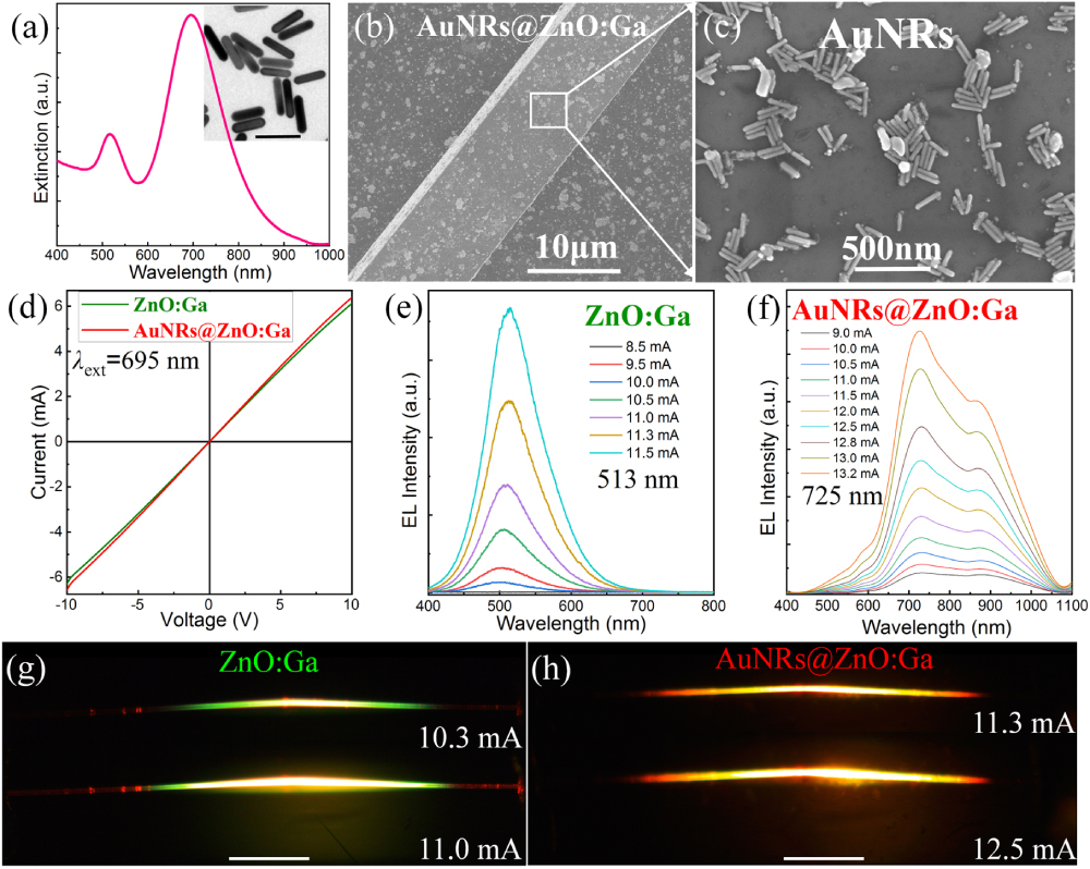
Figure 1.EL emission characteristics from single AuNRs@ZnO:Ga MW-based incandescent-type light source (the extinction peak of Au-nanorod, 695 nm). (a) The extinction spectrum of Au nanorods, with corresponding TEM image of the Au nanorods demonstrated in the inset. (b) SEM image of single AuNRs@ZnO:Ga MW. (c) Amplified SEM image of Au nanorods deposited on the MW. (d) characteristics of single ZnO:Ga MW prepared via Au nanorods decoration. (e) EL emission spectra from single ZnO:Ga MW-based fluorescent emitter. (f) EL emission spectra from single AuNRs@ZnO:Ga MW-based incandescent-type light source. (g) Optical microscopic image of the light emitting from electrically biased single ZnO:Ga MW-based fluorescent emitter (scale bar, 200 μm). (h) Optical microscopic image of the light emitting from electrically biased single AuNRs@ZnO:Ga MW-based incandescent-type light source (scale bar, 200 μm).
Especially when the injection current exceeded a certain value, such as 8.5 mA, green lighting can be observed, with the emission regions located at its center. Increasing the injection current can enhance its brightness, as well as expand the lighting regions. To further characterize the emission characteristics, Fig. 1(e) illustrates the EL spectra of the single ZnO:Ga MW based emitter, with the dominant emission peaks centered at 513 nm. Figure 1(g) presents an optical microscope photograph of the green emissions. Afterwards, introducing Au nanorods deposition, linear characteristics demonstrated that there was little effect on the modification of electronic transport characteristics, as demonstrated in Fig. 1(d) (the red solid line). With increasing injection current ranging from 9.0 to 13.2 mA, single AuNRs@ZnO:Ga MW-based incandescent-type lamp filament began to emit bright and red lighting, with the dominant emission peaks redshifting to about 725 nm, as shown in Fig. 1(f). Therefore, by incorporating Au nanorods, individual ZnO:Ga MW can be applied to construct near-infrared typical incandescent lamp filament source.
Considering the influence of Au nanorods on the modulation of typical near-infrared emissions, optical and electronic properties of single AuNRs@ZnO:Ga MW were measured. First, single ZnO:Ga MW with a quadrilateral cross section was synthesized via one-step carbothermal reduction methods. Figure 2(a) demonstrates the optical photograph of the as-synthesized ZnO:Ga MWs, indicating that a mass of MWs can be collected around the Si wafer. Figure 2(b) illustrates that the as-synthesized ZnO:Ga MW possessed smooth surfaces, accompanied with perfect quadrilateral cross section displayed in the inset. Therefore, individual ZnO:Ga MWs with quadrilateral cross section can be produced by a free catalyst via a vapor–solid process [40,48]. With the aid of a spin-coating technique, Au nanorods with random orientation can be deposited on the ZnO:Ga MW. Figure 2(c) illustrates the SEM image of the deposited Au nanorods. And then, Au nanorods with controlled aspect ratio ranging from panel I to panel IV were also synthesized, as demonstrated in Fig. 2(d). The extinction of Au nanorods was measured using an ultraviolet-visible-near-infrared spectrometer, as displayed in Fig. 2(e). It exhibited typically their ultraviolet-visible-near-infrared extinction spectra, each of which is composed of one transversal surface plasmon resonance peak centered around 510 nm, and the other longitudinal resonance peaks ranging from 600 nm (panel I), 695 nm (panel II), 783 nm (panel III), to 855 nm (panel IV) [7,41,49].

Figure 2.(a) Optical photograph of the synthesized ZnO:Ga MWs. (b) SEM image of single ZnO:Ga MW, with perfect quadrilateral cross section displayed in the inset (scale bar, 12 μm). (c) SEM image of ZnO:Ga MW prepared with Au nanorods decoration (the spin-coating number, ×1). (d) TEM images of the Au nanorods with controlled aspect ratio. (e) The extinction spectra of Au nanorods with controlled aspect ratio. (f) PL emissions from ZnO:Ga MW prepared via Au nanorods decoration, with the controlled aspect ratios. (g) behaviors of single ZnO:Ga MW prepared with Au nanorods decoration (corresponding extinction peak centered at 695 nm), with the spin-coating number ranging from 0 to 6.
Room-temperature PL measurements were carried out on account of single ZnO:Ga MW deposited via Au nanorods decoration. In the case of PL measurement, a single ZnO:Ga MW with the length up to 2 cm was selected, and then divided into four segments. PL emission of single bare ZnO:Ga MW displayed that ultraviolet emission centered around 378 nm dominated the PL spectra, accompanied with weak visible emission, as illustrated in Fig. 2(f). Thus, the PL emissions could be divided into two main bands: the dominant emission is the typical near-band-edge (NBE) ultraviolet emission, while the other negligible emission may be originated from the related broad deep levels, or related Ga incorporation induced impurity level emissions in the visible range [45,47,50]. By contrast, the enhancement of ultraviolet emission can be achieved by means of introducing Au nanorod deposition [Fig. 2(f)]. Compared with the bare ZnO:Ga MW, a little blueshift of PL emissions can be achieved, which could be ascribed to the electron filling of the conduction band of ZnO:Ga (Burstein–Moss effect). The remarkable enhancement of the NBE-type PL emission could be attributed to the charge transfer from Au nanorods to ZnO:Ga MWs [51–53]. Especially, by incorporating Au nanorods, near-infrared emission cannot be collected from optical pumping single AuNRs@ZnO:Ga MW. Therefore, under optical pumping excitation, Au nanorods with the extinction peak centered at 695 nm cannot be applied to achieve the realization of Au-nanorod plasmons selectively amplifying the near-infrared emissions from AuNRs@ZnO:Ga MWs.
To probe into influence of Au nanorods on the electronic transport properties, the deposition of Au nanorods on the MW was also taken into account by adjusting the spin coating. Again, the curves illustrated that introducing Au nanorods did have little effect on the electronic transport behavior of single ZnO:Ga MW, as shown in Fig. 2(g). Compared with metal nanostructure decoration by means of the physical sputtering technique, the little modulation on the electronic transport properties may be ascribed to the water solubility, and the remaining organics as well during the synthesizing process [17,19,54,55].
While introducing light illumination, the photoconductive behavior from single AuNRs@ZnO:Ga MW was characterized. The relevant schematic diagram is depicted in Fig. 3(a) [56–59]. In this section, Au nanorods [panel II in Fig. 2(d)] were utilized to construct single AuNRs@ZnO:Ga MW. By comparison, electrical characterizations were conducted to exploit the photoelectric properties of single AuNRs@ZnO:Ga MW under dark and lighting illumination, with the lasing wavelengths denoted as 405 nm, 532 nm, and 685 nm, respectively. Meanwhile, to guarantee that the photoconductive behavior of the single AuNRs@ZnO:Ga MW relied on the incident radiation wavelength, the laser power tuner was utilized to achieve the excitation laser intensity being . The single ZnO:Ga MW prepared with or without Au nanorod decoration can yield the dark current around 5.0 mA, and the photocurrent of 17.5 mA at 20 V, with the incident lasing wavelengths denoted as 405 nm and 532 nm, respectively. Especially when lighting is illuminated under the excitation laser at 685 nm, the characteristic curve of single AuNRs@ZnO:Ga MW demonstrated that the maximum photocurrent value of 31.5 mA can be detected, which is sixfold that of the bare ZnO:Ga MW, as demonstrated in Fig. 3(b) [17,37,39].
Figure 3.Photoconductive behavior of single AuNRs@ZnO:Ga MW [Au nanorod in Fig. 2(d) panel II, the extinction peak, 695 nm]. (a) Schematic diagram of hot carrier generation mechanisms in plasmonic Au nanorods, and then injected into ZnO:Ga MW channel under light illumination. (b) The characteristics of single ZnO:Ga MW prepared with Au nanorods decoration under dark, and illumination with the excitation lasing wavelengths at 405 nm, 532 nm, and 685 nm, respectively, with the laser power density denoted as . (c) The characteristics with on/off switching under light illumination, with the lasing wavelengths at 405 nm, 532 nm, and 685 nm, respectively. (d) UV-vis absorption spectra of the as-synthesized ZnO:Ga MWs prepared with and without Au nanorods deposition. (e) The comparison of TRPL decays from single bare ZnO:Ga MW, and Au nanorods decorated ZnO:Ga MW. (f) Diagrammatic drawing of the physical process involving (i) photoexcitation induced electrons and (ii) plasmons induced generation, injection, or tunneling procedure of hot electrons towards the interface between Au-ZnO:Ga under light illumination.
In addition, the time-dependent photocurrent curves of single AuNRs@ZnO:Ga MW (the extinction peak, 695 nm) with on/off switching upon light illumination at zero bias voltage are shown in Fig. 3(c). When illuminated at 405 nm and 532 nm, respectively, the detected photocurrent spectra demonstrated a sharp increase in intensities, which is concomitant with the onset of illumination. Accordingly, the maximum photoconductivity values of 2.1 nA and 2.5 nA were detected, respectively. While introducing the lasing illumination at 685 nm, a photocurrent around 5.20 nA can be detected. To rule out that the detected photocurrent response may be generated from the presence of surface defects, such as antisite oxide , Zn vacancy , oxygen vacancy , and Ga substituted Zn , time-dependent photocurrent characteristics were also studied on the base of single bare ZnO:Ga MW, but little signal of the photocurrent could be detected [39,58,59]. The detected photocurrent response at the excitation laser of 405 and 532 nm may be originated from directly photoexcited carrier generation due to the absorption of the deposited Au nanorods. That is, under direct photoexcitation, carriers could be collected from the excitation of d-band, which is well below the Fermi level, and then they are transited into the conduction band in Au nanorod. By contrast, the higher photocurrent values detected at the illumination of lasing wavelength from single AuNRs@ZnO:Ga MW can be ascribed to Au-plasmon induced hot electron generation and injection towards the interface between Au nanorods and ZnO:Ga MW, since the wavelength of the incident light being 685 nm approximates the plasmon excitation energy of the deposited Au nanorods (1.78 eV) [2,17,60].
Afterwards, the typical absorption of single ZnO:Ga MW prepared with and without Au nanorods deposition was carried out, as shown in Fig. 3(d). A strong absorption in the ultraviolet spectral region can be observed, accompanied with negligible absorption in the spectral band from visible to near-infrared. It is also noted that by introducing Au nanorods decoration, a little enhancement of the ultraviolet absorption from AuNRs@ZnO:Ga MWs can be achieved. To characterize the modulation of Au-nanorods on the decay time of ZnO:Ga MW, time-resolved photoluminescence (TRPL) experiments were carried out using an optically triggered streak camera system (C10910, Hamamatsu) of the fundamental 35 fs pulses with a repetition rate of 1 kHz (OperA Solo, Coherent). Corresponding TRPL spectra were collected at the probe wavelength of 375 nm [56,58,59]. Figure 3(e) shows the TRPL spectra of single ZnO:Ga MW prepared with and without Au nanorods decoration. In contrast, the single bare ZnO:Ga MW displayed a monoexponential decay, with the lifetime . While introducing Au nanorod deposition, the exponential decay lifetime reduced to be about 21.0 ps. The shorter decay time can be attributed to the increased recombination rate of excitons, which is induced by Au nanorod plasmons. Additionally, the PL decay time of single AuNRs@ZnO:Ga MW can be expressed as , where and are nonradiative and radiative decay times of the hybrid architecture, respectively, and is the Au-plasmon mediated exciton lifetime. Due to the smaller , the spontaneous emission rate of single AuNRs@ZnO:Ga MW is higher than that of bare ZnO:Ga MW [53–55].
It is well-known that the hot carrier generation from metal nanostructures can be divided into two major physical mechanisms: direct photoexcitation and nonradiative plasmonic decay [60]. Direct photon absorption from metallic nanostructures could be utilized to produce a photocurrent; nevertheless, due to the small electron–photon cross section, the hot carrier generation is very inefficient. Additionally, the photoexcited carriers from Au nanorods are primarily dominated by interband transitions. Under lighting illumination, electrons can be excited, and then transited from the d-band with its upper edge below the Fermi level [8,28]. By comparing with direct photoexcitation, nonradiative plasmonic decaying inducing the generation of hot carrier facilitates the excitation of electrons from near the Fermi energy, leading to generation of hot electrons with substantially high energy. The hot electrons with adequate energy can overcome the metal–semiconductor barrier. Therefore, the hot carriers generated by surface plasmons are larger than that from interband transitions. It also indicated that plasmons decaying nonradiatively induced hot carrier generation could be more efficient [10,17,61].
To exploit the generation mechanism of photoinduced carriers from Au nanorods, a diagrammatic drawing is depicted in Fig. 3(f). For the incident light at the wavelengths being substantially deviated from excitation wavelengths of metal plasmons, the photocurrents detected are dominated by directly photoexcited carriers from Au nanorods, which are deposited on ZnO:Ga MW. The excited carriers generated are primarily from interband transitions: the excited electrons can be transited from the d-band to the conduction band above the Fermi level, with corresponding physical process denoted as i [see Fig. 3(f)]. Under radiation at 685 nm, which is in close proximity to the extinction wavelength of the Au nanorods, localized surface plasmons in Au nanorods can be excited. And then, by means of nonradiative plasmonic decay, the excited metal plasmons can transfer the energy to oscillating electrons, yielding the distribution of hot electrons, with the energy well above the Fermi level of Au. While possessing the energy well above the Schottky barrier towards the interface between Au-nanorod and ZnO:Ga, the generated hot electron can be directly injected into the conduction band of the neighboring ZnO:Ga MW; additionally, electrons with lower energies than the Fermi energy have exponentially decreased probability to be injected. The hot electron generation and injection processes denoted as ii in Fig. 3(f) can be responsible for the enhancement of the photocurrents, although, the directly photoexcited carrier injection process previously described is still allowed to occur [11,21,60].
Full-field electromagnetic simulations were also carried out using a commercially available software package, Lumerical FDTD. The metallic particles in this study are assumed to be Au nanorods, and are modeled by using experimental dielectric data [17,62]. During the simulation procedure, the Au nanorod with the length (50 nm) and diameter (20 nm) was adopted, accompanied with the resonant wavelength denoted as , the refractive index of ZnO:Ga denoted as , and the refractive index of environmental medium air denoted as . Electrical field intensity distribution of isolated Au nanorods can be calculated, with the electromagnetic wave propagating along the direction of plane [Fig. 4(a)], the direction of the plane [Fig. 4(b)], and the direction of the plane [Fig. 4(c)]. Thus, the total -field intensities can be calculated in accordance with resonance wavelength, with corresponding field intensities localized towards the contact region between Au-nanorod and ZnO:Ga MW. In particular, single Au nanorods can exhibit much stronger field localization around the contact regions. Electromagnetic energy could be confined to the Au-ZnO:Ga junctions, giving rise to intense localized -field.
Figure 4.Electrical field intensity distribution of isolated Au-nanorods, with the electromagnetic wave propagating along (a) the direction of the plane (horizontal), (b) the direction of the plane (vertical), and (c) the direction of the plane (horizontal). In the simulation process, Au-nanorods with the length (50 nm) and diameter (20 nm) were adopted, accompanied with the resonant wavelength denoted as , the refractive index of ZnO:Ga denoted as , and the refractive index of environmental medium air .
As we previously stated above, Au nanorods with the extinction peak centered at 695 nm can be utilized to construct near-infrared incandescent-type light sources from electrically biased single AuNRs@ZnO:Ga MW based incandescent-type lamp filament. Meanwhile, the dominant emission peaks relate to the plasmons of Au nanorods, accompanied with strong electric field localizations towards the deposition areas of Au-nanorods. Additionally, PL emission measurements from single AuNRs@ZnO:Ga MW also demonstrated that the enhancement of the ultraviolet emission can be attributed to cooperative effect of the suppression of the visible emission and Au-nanorod plasmons induced hot electron generation and injection from Au nanorods into the conduction band of ZnO:Ga [53,54,63]. Due to the mismatching between the extinction peaks of Au-nanorods and the negligible PL emission in the near-infrared spectral band of single MW, the electrically driven near-infrared emissions cannot be attributed to Au-nanorod plasmon selectively amplified near-infrared emission from single bare ZnO:Ga MW. To exploit the remarkable modulation of near-infrared emission behavior from an electrically driven single AuNRs@ZnO:Ga MW based filament-type light source, a diagrammatic drawing is depicted in Fig. 5(a). Single bare ZnO:Ga MW can be utilized to construct semiconducting filament emitter. While introducing Au nanorods deposition, the intrinsic lighting from a single bare ZnO:Ga MW based emitter can be completely suppressed. Therefore, Au-nanorods nonradiatively inducing the interfacial energy transfer between Au-nanorod and ZnO:Ga MW can occur [17,64,65].
Figure 5.(a) Schematic illustration of the modulation of Au-nanorod plasmons on the incandescent-type lighting features of single ZnO:Ga MW-based fluorescent light source. (b) Normalized intensities of the EL spectrum from single bare ZnO:Ga MW-based fluorescent light source, the EL spectrum from single AuNRs@ZnO:Ga MW-based fluorescent light source, and the extinction spectrum of the deposited Au nanorods. (c) Micrographs of bright visible light emitting from an electrically driven single AuNRs@ZnO:Ga MW-based incandescent-type light source in the dark field and bright field (scale bar, 200 μm). (d) Optical microscopic images of bright visible light emitting from electrically driven single ZnO:Ga MW prepared with partial Au nanorods decoration (scale bar, 300 μm).
Despite the excitation energy sufficiently large above the Fermi level and thus the nonradiative plasmonic decay, with the relaxation time in the order of the nanosecond to millisecond rate, nonequilibrium hot electron distribution can be produced [8,10,16,66]. However, electrically driving the generation of nonthermalized hot carriers is still at the primary stage. That is, to explore the likelihood of electrically driving the generation of nonequilibrium hot electrons from single AuNRs@ZnO:Ga MW, normalized intensities consisting of the extinction spectrum of Au nanorods, EL emission spectrum of the single bare ZnO:Ga MW-based emitter, and EL emission spectrum from single AuNRs@ZnO:Ga MW-based emitter were depicted, as shown in Fig. 5(b). The spectral overlap between transversal plasmon resonance peak of Au nanorods and EL emission spectra from a single ZnO:Ga MW-based incandescent-type source was achieved in the visible spectral band. By incorporating Au nanorods, the incandescent-type lighting features from a single MW-based filament emitter illustrated that the dominating lighting peaks redshifted to around 725 nm. Interestingly, remarkable overlapping between the longitudinal resonance peak and incandescent-type lighting peak from single AuNRs@ZnO:Ga MW-based filament emitter was also observed. Thus, under electrical driving, the near-infrared incandescent-type lighting cannot be assigned to the PLs from the Au nanorods, which are deposited on the MWs [7,30,33,67].
To further exhibit the modulation of Au-nanorods on the emission characteristics of a single ZnO:Ga MW-based filament-type emitter, a single ZnO:Ga MW with the length was selected, and by introducing Au nanorods [panel II in Fig. 2(d)] decoration uniformly, remarkably bright visible emissions were also observed from the wire once the applied bias exceeded a certain value, as demonstrated in Fig. 5(c). And, its brightness increased with the applied bias. By contrast, another ZnO:Ga MW with the length was also selected, and then Au nanorods [panel II in Fig. 2(d)] partially deposited on the MW were introduced, as demonstrated in Fig. 5(d). When the applied bias reached a certain value, such as 44 V, bright and visible emission can be observed, with the red lighting regions located towards the section, where Au nanorods were deposited. The most interesting finding is that bright and green emission can also be observed, with the emission regions located towards the bare segment [see Fig. 5(d)]. Therefore, tandem emission units involving green and red emissions can be constructed.
The incandescent-type lighting working mechanism is depicted in Fig. 6 [19,35]. First, being electrically driven, the hottest spots can also be formed towards the center of the MW prepared with Au nanorod decoration due to the Joule heating effect. Thus, a sufficiently strong electric field () could be produced towards the hottest spots owing to the extremely poor heat dissipation, which is induced by high crystallization quality of the as-synthesized MWs [45,68–70]. Second, the transported electrons in the MW channel can be accelerated and become energized electrons, which are spatially localized towards the center of the MW. Because of the inelastic collision, the interplay of the energized electrons transported in the MW channel and free electrons localized at the surface of Au-nanorod can occur. In consequence, collective oscillation of the free electrons in Au nanorods can be excited [65,69,71]. Finally, through nonradiative plasmonic decay, Au-nanorod plasmons can transfer their energies into oscillating higher-energy electrons, leading to formation of hot electrons. Considering that the nonthermal distribution of the hot electrons is well above the Fermi energy of Au-nanorods, the energetic electron with its energies above the contact-potential barrier at the metal–semiconductor interface is directly injected in the conduction band of the adjacent ZnO:Ga MW, while the electrons with relative lower energies have an exponentially decreased probability to be injected [17,29,67]. Especially once the hot electron possessed the energy up to plasmon frequency, Au-nanorod plasmons inducing the generation of nonequilibrium distribution of hot electrons can lead to the state-filling effect in the energy-level configuration of ZnO:Ga, which can be employed to dominate the near-infrared emission characteristics from single AuNRs@ZnO:Ga MW-based incandescent light source [8,54,55].
Figure 6.Schematic diagram of the working principle of bright visible light emitting from electrically biased single AuNRs@ZnO:Ga MW-based incandescent-type light source.
To probe into the near-infrared incandescent-type emission features, it can also be found out that the hot carrier transfer rate is being higher than its relaxation rate in the single AuNRs@ZnO:Ga MW, accompanied with the nonequilibrium hot electron in the conduction band with its energy up to plasmon frequency. After relaxation of the nonequilibrium hot electrons, another energy level may be created in the energy-level configuration of ZnO:Ga, resulting in the thermal and nonthermal distributions overlap in population. Therefore, during this relaxation, fractional electrons could be scattered into energy-level configuration of ZnO:Ga (luminescent states), where they can recombine with holes in the form of emitting photons. It is reasonable to deduce that the dominating emission wavelength of the emitted photons is relevant to the energies of the hot electrons, and then redshifts monotonically after the relaxation procedure. The generation and injection of hot electrons with energy up to the plasmon frequency can be utilized to dominate the characteristic of the emitted photons, such as the emission wavelength and spectral linewidth [8,27,30,66]. Despite that, Joule heating effect played a significant role in the incandescent-type emission characteristics, but it cannot be compatible with the thermal radiation mechanism (blackbody radiation theory). By comparing the emission spectra collected from the single AuNRs@ZnO:Ga MW-based incandescent-type light source and the corresponding emission peaks from the theoretical models of blackbody radiation, the maximum temperatures were calculated and can approach 3000 K, which far more greatly exceeded the endurance of single ZnO:Ga MW [68,69]. In addition, for the emission characteristics, such as wavelength-tuning emission from individual ZnO:Ga MW-based light sources heavily depending on the Ga-incorporation concentration, increasing the injection current can bring a little redshift of the dominating emission peaks, while reducing the ambient temperature can bring significant enhancement of the EL emissions and so on, and can also rule out the thermal radiation mechanism. Therefore, there is no direct experimental evidence that the incandescent-type lighting characteristics, such as the emission wavelengths, spectral linewidth, and the incandescent-type lighting output intensity, were dominated by the temperature generated by the Joule heating effect [19,45,69,70].
By introducing Au nanorods with controlled aspect ratio deposition, a near-infrared filament-type light source composed of individual ZnO:Ga MWs was fabricated. Taking single ZnO:Ga MW prepared via Au nanorod [panel I in Fig. 2(d), with the extinction peak centered at 605 nm] decoration for example, Fig. 7(a) demonstrates that a little enhancement of electronic transport properties can be obtained. By comparison, the dominant emission peaks centered at 527 nm were observed from electrically driven single bare ZnO:Ga MW-based incandescent-type lamp filament, as illustrated in Fig. 7(b). Introducing Au nanorod deposition, the dominating emission peaks redshifted to around 601 nm, as shown in Fig. 7(c). While introducing Au nanorod decoration [panel III in Fig. 2(d), with the extinction peak centered around 783 nm], the incandescent-type emissions from single ZnO:Ga MW-based filament light source also redshifted, with the dominating emission peaks centered around 780 nm, as indicated in Figs. 7(e) and 7(f). When Au nanorods [panel IV in Fig. 2(d)] with the extinction peak centered around 850 nm were deposited on the synthesized MW, EL emission characteristics displayed that the dominant emission peaks from the bare ZnO:Ga MW-based filament light source centered at 513 nm redshifted to about 905 nm, as demonstrated in Figs. 7(h) and 7(i). Therefore, by introducing Au nanorods with controlled aspect ratio decoration, wavelength-tunable incandescent-type emissions from individual ZnO:Ga MWs-based filament-type light sources can be realized, with the dominant emission peaks tuning from visible to near-infrared spectral band.
Figure 7.Wavelength-tunable emissions from single AuNRs@ZnO:Ga MW-based incandescent-type light source: (a) characteristics of single ZnO:Ga MW via Au nanorods decoration (the extinction peak, 605 nm); (b) EL emission from single bare ZnO:Ga MW-based incandescent-type light source, with the emission wavelength centered at 527 nm; (c) EL emission from single AuNRs@ZnO:Ga MW-based incandescent-type light source, with the emission wavelength centered at 601 nm. (d) characteristics of single ZnO:Ga MW prepared via Au nanorods decoration (the extinction peak, 783 nm); (e) EL emission from single bare ZnO:Ga MW-based incandescent-type light source, with the emission wavelength centered at 518 nm; (f) EL emission from the single AuNRs@ZnO:Ga MW-based incandescent-type light source, with the emission wavelength centered around 780 nm. (g) characteristics of single ZnO:Ga MW via Au nanorods decoration (the extinction peak, 855 nm); (h) EL emission from the single bare ZnO:Ga MW-based incandescent-type light source, with the emission wavelength centered at 513 nm; (i) EL emission from the single AuNRs@ZnO:Ga MW-based incandescent-type light source, with the emission wavelength centered around 905 nm.
Consequently, incandescent-type light sources can be achieved from single semiconducting nano/MWs prepared via metal nanostructure decoration. It also can offer manageable, predictable, and ongoing requirements to construct electrically driven ultracompact optoelectronic devices. This experimental scheme can be extended to other wide bandgap semiconductors, such as GaN, , and . Especially, by introducing metal nanostructure deposition, the typical light sources with the emission wavelengths may cover from ultraviolet to near-infrared spectral band. Being integrated as single- or multicolor emission units, the incandescent-type light sources can be compatible with silicon-based photonics and optoelectronics devices, as well as lab-on-chip devices. Furthermore, some scientific and technical challenges still remain, and need to be addressed to realize this potential, such as the development of electrically driving the generation of nonequilibrium hot carrier schemes with higher efficiency, and hot-electron-induced fabrication of tunneling diodes [35,67,69,71,72].
4. CONCLUSION
In summary, typical incandescent light sources were successfully constructed on account of individual AuNRs@ZnO:Ga MWs. By adjusting the aspect ratios of the Au nanorods, wavelength-tunable incandescent-type emissions can be achieved, with the dominating lighting wavelengths tuned from visible to near-infrared spectral bands. The intrinsic physical mechanisms being responsible for the emission modulation can be attributed to Au-plasmon-induced generation of nonequilibrium hot electrons that then are injected into the neighboring ZnO:Ga. Due to nonthermal distribution of the hot electrons with energy up to the plasmon frequency, the state-filling effect can be formed in the energy-level configuration. In particular, the experimental results represented further important progress to overcome the limitation of the bandgap of semiconductors involving electrically driving the generation and injection of energetically tunable, nonequilibrium distribution of hot electrons, plasmons mediated energy transfer, and the nonequilibrium hot-carrier-induced state-filling effect. Additionally, wavelength-tunable emission realized from individual MWs prepared with metal nanostructure decoration can overcome the traditional dilemma of semiconducting light sources with sophisticated fabrication technologies associated with p–n junctions, Schottky junctions, bandgap engineering, and so on. Consequently, the novel incandescent-type light sources may find potential applications in integrated optoelectronic devices, such as multicolor emission devices and electric spasers.
References
[1] X. Li, J. Zhu, B. Wei. Hybrid nanostructures of metal/two-dimensional nanomaterials for plasmon-enhanced applications. Chem. Soc. Rev., 45, 3145-3187(2016).
[2] Z. Yang, K. Du, F. Lu, Y. Pang, S. Hua, X. Gan, W. Zhang, S. J. Chua, T. Mei. Silica nanocone array as a template for fabricating a plasmon induced hot electron photodetector. Photon. Res., 7, 294-299(2019).
[3] P. Wang, A. V. Krasavin, M. E. Nasir, W. Dickson, A. V. Zayats. Reactive tunnel junctions in electrically driven plasmonic nanorod metamaterials. Nat. Nanotechnol., 13, 159-164(2018).
[4] I. F. Teixeira, E. C. M. Barbosa, S. C. E. Tsang, P. H. C. Camargo. Carbon nitrides and metal nanoparticles: from controlled synthesis to design principles for improved photocatalysis. Chem. Soc. Rev., 47, 7783-7817(2018).
[5] K. Zhang, Y. Liu, J. Zhao, B. Liu. Nanoscale tracking plasmon-driven photocatalysis in individual nanojunctions by vibrational spectroscopy. Nanoscale, 10, 21742-21747(2018).
[6] S. Kahmann, M. A. Loi. Hot carrier solar cells and the potential of perovskites for breaking the Shockley–Queisser limit. J. Mater. Chem. C, 7, 2471-2486(2019).
[7] B. Huang, Z. Kang, J. Li, M. Liu, P. Tang, L. Miao, C. Zhao, G. Qin, W. Qin, S. Wen, P. N. Prasad. Broadband mid-infrared nonlinear optical modulator enabled by gold nanorods: towards the mid-infrared regime. Photon. Res., 7, 699-704(2019).
[8] S. K. Cushing, C. J. Chen, C. L. Dong, X. T. Kong, A. O. Govorov, R. S. Liu, N. Wu. Tunable nonthermal distribution of hot electrons in a semiconductor injected from a plasmonic gold nanostructure. ACS Nano, 12, 7117-7126(2018).
[9] S. Tan, A. Argondizzo, J. Ren, L. Liu, Z. Jin, H. Petek. Plasmonic coupling at a metal/semiconductor interface. Nat. Photonics, 11, 806-812(2017).
[10] S. Tan, Y. Dai, S. Zhang, L. Liu, J. Zhao, H. Petek. Coherent electron transfer at the Ag/graphite heterojunction interface. Phys. Rev. Lett., 120, 126801(2018).
[11] R. Sundararaman, P. Narang, A. S. Jermyn, H. A. Atwater. Theoretical predictions for hot-carrier generation from surface plasmon decay. Nat. Commun., 5, 5788(2014).
[12] J. Feng, C. Gao, Y. Ying. Nanoscale tracking plasmon-driven photocatalysis in individual nanojunctions by vibrational spectroscopy. Nanoscale, 10, 20492-20504(2018).
[13] A. M. Brown, R. Sundararaman, P. Narang, H. A. Atwater. Nonradiative plasmon decay and hot carrier dynamics: effects of phonons, surfaces, and geometry. ACS Nano, 10, 957-966(2015).
[14] H. Lee, J. Lim, C. Lee, S. Back, K. An, J. W. Shin, R. Ryoo, Y. Jung, J. Y. Park. Boosting hot electron flux and catalytic activity at metal-oxide interfaces of PtCo bimetallic nanoparticles. Nat. Commun., 9, 2335(2018).
[15] T. Mohammad, T. Hossein, X. Zihao, L. Kyu-Tae, R. Sean, Y. Jiahao, A. Ali, L. Tianquan, C. Wenshan. Ultrafast control of phase and polarization of light expedited by hot electron transfer. Nano Lett., 18, 5544-5551(2018).
[16] S. A. K. Cushing. Plasmonic hot carriers skip out in femtoseconds. Nat. Photonics, 11, 748-749(2017).
[17] A. Pescaglini, A. Martin, D. Cammi, G. Juska, C. Ronning, E. Pelucchi, D. Iacopino. Hot-electron injection in Au nanorod-ZnO nanowire hybrid device for near-infrared photodetection. Nano Lett., 14, 6202-6209(2014).
[18] G. Lozano, S. R. Rodriguez, M. A. Verschuuren, J. G. Rivas. Metallic nanostructures for efficient led lighting. Light Sci. Appl., 5, e16080(2016).
[19] Y. Liu, M. Jiang, Z. Zhang, B. Li, H. Zhao, C. Shan, D. Shen. Electrically excited hot-electron dominated fluorescent emitters using individual Ga-doped ZnO microwires via metal quasiparticle film decoration. Nanoscale, 10, 5678-5688(2018).
[20] J. H. Park, Y. K. Dong, E. F. Schubert, J. Cho, J. K. Kim. Fundamental limitations of wide-bandgap semiconductors for light-emitting diodes. ACS Energy Lett., 3, 655-662(2018).
[21] P. Zilio, M. Dipalo, F. Tantussi, G. C. Messina, F. D. Angelis. Hot electrons in water: injection and ponderomotive acceleration by means of plasmonic nanoelectrodes. Light Sci. Appl., 6, e17002(2017).
[22] S. Wang, J. Wang, W. Zhao, F. Giustiniano, L. Chu, I. Verzhbitskiy, Y. J. Zhou, G. Eda. Efficient carrier-to-exciton conversion in field emission tunnel diodes based on MIS-type van der Waals heterostack. Nano Lett., 17, 5156-5162(2017).
[23] B. Palash, B. Alexandre, N. Lukas. Electrical excitation of surface plasmons. Phys. Rev. Lett., 106, 226802(2011).
[24] W. Cai, R. Sainidou, J. Xu, A. Polman, F. J. G. de Abajo. Efficient generation of propagating plasmons by electron beams. Nano Lett., 9, 1176-1181(2009).
[25] H. Wei, D. Pan, S. Zhang, Z. Li, Q. Li, N. Liu, W. Wang, H. Xu. Plasmon waveguiding in nanowires. Chem. Rev., 118, 2882-2926(2018).
[26] M. Cohen, Y. Abulafia, R. Shavit, Z. Zalevsky. Secondary electron imaging of light at the nanoscale. ACS Nano, 11, 3274-3281(2017).
[27] M. Buret, A. V. Uskov, J. Dellinger, N. Cazier, M.-M. Mennemanteuil, J. Berthelot, I. V. Smetanin, I. E. Protsenko, G. Colas-des Francs, A. Bouhelier. Spontaneous hot-electron light emission from electron-fed optical antennas. Nano Lett., 15, 5811-5818(2015).
[28] S. Ganti, P. J. King, E. Arac, K. Dawson, M. J. Heikkil, J. H. Quilter, B. Murdoch, P. Cumpson, A. O’Neill. Voltage controlled hot carrier injection enables ohmic contacts using Au island metal films on Ge. ACS Appl. Mater. Interfaces, 9, 27357-27364(2017).
[29] M. K. Seo, K. C. Huang, M. L. Brongersma. Electrically driven subwavelength optical nanocircuits. Nat. Photonics, 8, 244-249(2014).
[30] Y. Y. Cai, J. G. Liu, L. J. Tauzin, D. Huang, E. Sung, H. Zhang, A. Joplin, W. S. Chang, P. Nordlander, S. Link. Photoluminescence of gold nanorods: Purcell effect enhanced emission from hot carriers. ACS Nano, 12, 976-985(2018).
[31] G. Wei, B. Xu, H. L. Dai. Super bright luminescent metallic nanoparticles. J. Phys. Chem. Lett., 9, 4155-4159(2018).
[32] S. Kahmann, M. A. Loi. Plexcitonics — fundamental principles and optoelectronic applications. J. Mater. Chem. C, 7, 1821-1853(2019).
[33] Y. Fang, W.-S. Chang, B. Willingham, P. Swanglap, S. Dominguez-Medina, S. Link. Plasmon emission quantum yield of single gold nanorods as a function of aspect ratio. ACS Nano, 6, 7177-7184(2012).
[34] S. Tan, L. Liu, Y. Dai, J. Ren, J. Zhao, H. Petek. Ultrafast plasmon-enhanced hot electron generation at Ag nanocluster/graphite heterojunctions. J. Am. Chem. Soc., 139, 6160-6168(2017).
[35] C. Karnetzky, P. Zimmermann, C. Trummer, C. D. Sierra, W. Martin, R. Kienberger, A. Holleitner. Towards femtosecond on-chip electronics based on plasmonic hot electron nano-emitters. Nat. Commun., 9, 2471(2018).
[36] R.-J. Shiue, Y. Gao, C. Tan, C. Peng, J. Zheng, D. K. Efetov, Y. D. Kim, J. Hone, D. Englund. Thermal radiation control from hot graphene electrons coupled to a photonic crystal nanocavity. Nat. Commun., 10, 109(2019).
[37] B. Zhao, W. Fei, H. Chen, L. Zheng, L. Su, D. Zhao, X. Fang. An ultrahigh responsivity (9.7 mA·W–1) self-powered solar-blind photodetector based on individual ZnO-Ga2O3 heterostructures. Adv. Funct. Mater., 27, 1700264(2017).
[38] G. H. He, M. M. Jiang, L. Dong, Z. Zhang, D. Shen. Near-infrared light-emitting devices from individual heavily Ga-doped ZnO microwires. J. Mater. Chem. C, 5, 2542-2551(2017).
[39] B. Zhao, F. Wang, H. Chen, Y. Wang, M. Jiang, X. Fang, D. Zhao. Solar-blind avalanche photodetector based on single ZnO-Ga2O3 core-shell microwire. Nano Lett., 15, 3988-3993(2015).
[40] M. Ding, D. Zhao, B. Yao, E. Shulin, Z. Guo, L. Zhang, D. Shen. The ultraviolet laser from individual ZnO microwire with quadrate cross section. Opt. Express, 20, 13657-13662(2012).
[41] Y. Ni, C. Kan, L. He, X. Zhu, M. Jiang, D. Shi. Alloyed Au-Ag nanorods with desired plasmonic properties and stability in harsh environments. Photon. Res., 7, 558-565(2019).
[42] W. Zhang, M. Caldarola, B. Pradhan, M. Orrit. Gold nanorod enhanced fluorescence enables single-molecule electrochemistry of methylene blue. Angew. Chem., 129, 3620-3623(2017).
[43] P. Pramod, K. G. Thomas. Plasmon coupling in dimers of Au nanorods. Adv. Mater., 20, 4300-4305(2008).
[44] C.-C. Hou, H.-M. Chen, J.-C. Zhang, N. Zhuo, Y.-Q. Huang, R. A. Hogg, D. T. Childs, J.-Q. Ning, Z.-G. Wang, F.-Q. Liu, Z.-Y. Zhang. Near-infrared and mid-infrared semiconductor broadband light emitters. Light Sci. Appl., 7, 17170(2018).
[45] M. Jiang, G. He, H. Chen, Z. Zhang, L. Zheng, C. Shan, D. Shen, X. Fang. Wavelength-tunable electroluminescent light sources from individual Ga-doped ZnO microwires. Small, 13, 1604034(2017).
[46] Y. Nishijima, K. Ueno, Y. Yokota, K. Murakoshi, H. Misawa. Plasmon-assisted photocurrent generation from visible to near-infrared wavelength using a Au-nanorods/TiO2 electrode. J. Phys. Chem. Lett., 1, 2031-2036(2010).
[47] G. D. Yuan, W. J. Zhang, J. S. Jie, X. Fan, J. X. Tang, I. Shafiq, Z. Z. Ye, C. S. Lee, S. T. Lee. Tunable n-type conductivity and transport properties of Ga-doped ZnO nanowire arrays. Adv. Mater., 20, 168-173(2008).
[48] M. Jiang, W. Mao, X. Zhou, C. Kan, D. Shi. Wavelength-tunable waveguide emissions from electrically driven single ZnO/ZnO:Ga superlattice microwires. ACS Appl. Mater. Interfaces, 11, 11800-11811(2019).
[49] F. Kim, J. H. Song, P. Yang. Photochemical synthesis of gold nanorods. J. Am. Chem. Soc., 124, 14316-14317(2002).
[50] W. T. Ruane, K. M. Johansen, K. D. Leedy, D. C. Look, W. H. Von, M. Grundmann, G. C. Farlow, L. J. Brillson. Defect segregation and optical emission in ZnO nano- and microwires. Nanoscale, 8, 7631-7637(2016).
[51] X. Liu, Q. Zhang, J. N. Yip, Q. Xiong, T. C. Sum. Wavelength tunable single nanowire lasers based on surface plasmon polariton enhanced Burstein–Moss effect. Nano Lett., 13, 5336-5343(2013).
[52] Y. Liu, M. Jiang, G. He, S. Li, Z. Zhang, B. Li, H. Zhao, C. Shan, D. Z. Shen. Wavelength-tunable ultraviolet electroluminescence from Ga-doped ZnO microwires. ACS Appl. Mater. Interfaces, 9, 40743-40751(2017).
[53] F. F. Qin, C. X. Xu, Q. X. Zhu, J. F. Lu, D. T. You, W. Xu, Z. Zhu, A. G. Manohari, F. Chen. Extra green light induced ZnO ultraviolet lasing enhancement assisted by Au surface plasmons. Nanoscale, 10, 623-627(2017).
[54] C. De Melo, M. Jullien, Y. Battie, A. En Naciri, J. Ghanbaja, F. Montaigne, J. F. Pierson, F. Rigoni, N. Almqvist, A. Vomiero, S. Migot, F. Mucklich, D. Horwat. Tunable localized surface plasmon resonance and broadband visible photoresponse of Cu nanoparticles/ZnO surfaces. ACS Appl. Mater. Interfaces, 10, 40958-40965(2018).
[55] S. Liu, M.-Y. Li, D. Su, M. Yu, H. Kan, H. Liu, X. Wang, S. Jiang. Broadband high sensitivity ZnO colloidal quantum dots/self-assembled Au nanoantennas heterostructures photodetectors. ACS Appl. Mater. Interfaces, 10, 32516-32525(2018).
[56] Z. Zhang, Y. Ning, X. Fang. From nanofibers to ordered ZnO/NiO heterojunction arrays for self-powered and transparent UV photodetectors. J. Mater. Chem. C, 7, 223-229(2019).
[57] W. Xu, Y. Shi, F. Ren, D. Zhou, L. Su, Q. Liu, L. Cheng, J. Ye, D. Chen, R. Zhang, Y. Zheng, H. Lu. Magnesium ion-implantation-based gallium nitride p-i-n photodiode for visible-blind ultraviolet detection. Photon. Res., 7, B48-B54(2019).
[58] K. Hu, F. Teng, L. Zheng, P. Yu, Z. Zhang, H. Chen, X. Fang. Binary response Se/ZnO p-n heterojunction UV photodetector with high on/off ratio and fast speed. Laser Photon. Rev., 11, 1600257(2017).
[59] Y. Ning, Z. Zhang, F. Teng, X. Fang. Novel transparent and self-powered UV photodetector based on crossed ZnO nanofiber array homojunction. Small, 14, 1703754(2018).
[60] B. Y. Zheng, H. Zhao, A. Manjavacas, M. McClain, P. Nordlander, N. J. Halas. Distinguishing between plasmon-induced and photoexcited carriers in a device geometry. Nat. Commun., 6, 7797(2015).
[61] A. Sobhani, M. W. Knight, Y. Wang, B. Zheng, N. S. King, L. V. Brown, Z. Fang, P. Nordlander, N. J. Halas. Narrowband photodetection in the near-infrared with a plasmon-induced hot electron device. Nat. Commun., 4, 1643(2013).
[62] P. B. Johnson, R.-W. Christy. Optical constants of the noble metals. Phys. Rev. B, 6, 4370-4379(1972).
[63] N. Han, F. Wang, J. J. Hou, S. P. Yip, H. Lin, F. Xiu, M. Fang, Z. Yang, X. Shi, G. Dong, T. F. Hung, J. C. Ho. Tunable electronic transport properties of metal-cluster-decorated III–V nanowire transistors. Adv. Mater., 25, 4445-4451(2013).
[64] H. Shan, Y. Yu, X. Wang, Y. Luo, S. Zu, B. Du, T. Han, B. Li, Y. Li, J. Wu, F. Lin, K. Shi, B. K. Tay, Z. Liu, X. Zhu, Z. Fang. Direct observation of ultrafast plasmonic hot electron transfer in the strong coupling regime. Light Sci. Appl., 8, 9(2019).
[65] K. H. Shokri, J. H. Yun, Y. Paik, J. Kim, W. A. Anderson, S. J. Kim. Plasmon field effect transistor for plasmon to electric conversion and amplification. Nano Lett., 16, 250-254(2015).
[66] T. Heilpern, M. Manjare, A. O. Govorov, G. P. Wiederrecht, S. K. Gray, H. Harutyunyan. Determination of hot carrier energy distributions from inversion of ultrafast pump-probe reflectivity measurements. Nat. Commun., 9, 1853(2018).
[67] S. P. Gurunarayanan, N. Verellen, V. S. Zharinov, F. James Shirley, V. V. Moshchalkov, M. Heyns, J. Van de Vondel, I. P. Radu, P. Van Dorpe. Electrically driven unidirectional optical nanoantennas. Nano Lett., 17, 7433-7439(2017).
[68] J. Zhao, H. Sun, S. Dai, Y. Wang, J. Zhu. Electrical breakdown of nanowires. Nano Lett., 11, 4647-4651(2011).
[69] Y. D. Kim, H. Kim, Y. Cho, J. H. Ryoo, C.-H. Park, P. Kim, Y. S. Kim, S. Lee, Y. Li, S.-N. Park, Y. S. Yoo, D. Yoon, V. E. Dorgan, E. Pop, T. F. Heinz, J. Hone, S.-H. Chun, H. Cheong, S. W. Lee, M.-H. Bae, Y. D. Park. Bright visible light emission from graphene. Nat. Nanotechnol., 10, 676-682(2015).
[70] G. H. He, M. M. Jiang, Z. Zhang, B. H. Li, H. Zhao, C. X. Shan, D. Shen. Sb-doped ZnO microwires: emitting filament and homojunction light-emitting diodes. J. Mater. Chem. C, 5, 10938-10946(2017).
[71] P. Rai, N. Hartmann, J. Berthelot, J. Arocas, G. C. des Francs, A. Hartschuh, A. Bouhelier. Electrical excitation of surface plasmons by an individual carbon nanotube transistor. Phys. Rev. Lett., 111, 026804(2013).
[72] T. A. Growden, W. Zhang, E. R. Brown, D. F. Storm, D. J. Meyer, P. R. Berger. Near-UV electroluminescence in unipolar-doped, bipolar-tunneling GaN/AlN heterostructures. Light. Sci. Appl., 7, 17150(2018).


