• Acta Optica Sinica
  • Vol. 38, Issue 7, 0724002 (2018)
Yanjun Sun1、*, Jun Wang1, Xuesong Ji2, Li Wang1, Yue Wang1, and Zhe Li1
Author Affiliations
  • 1 School of Opto-Electronic Engineering, Changchun University of Science and Technology, Changchun, Jilin 130022, China
  • 2 Liaoshen Industrial Group Co., Ltd., Shenyang, Liaoning 110045, China
  • show less
    DOI: 10.3788/AOS201838.0724002 Cite this Article Set citation alerts
    Yanjun Sun, Jun Wang, Xuesong Ji, Li Wang, Yue Wang, Zhe Li. Simulation and Experiment of Grooved Grating Microstructure for Infrared Chromatic Aberration Correction[J]. Acta Optica Sinica, 2018, 38(7): 0724002 Copy Citation Text show less
    Grooved grating microstructure
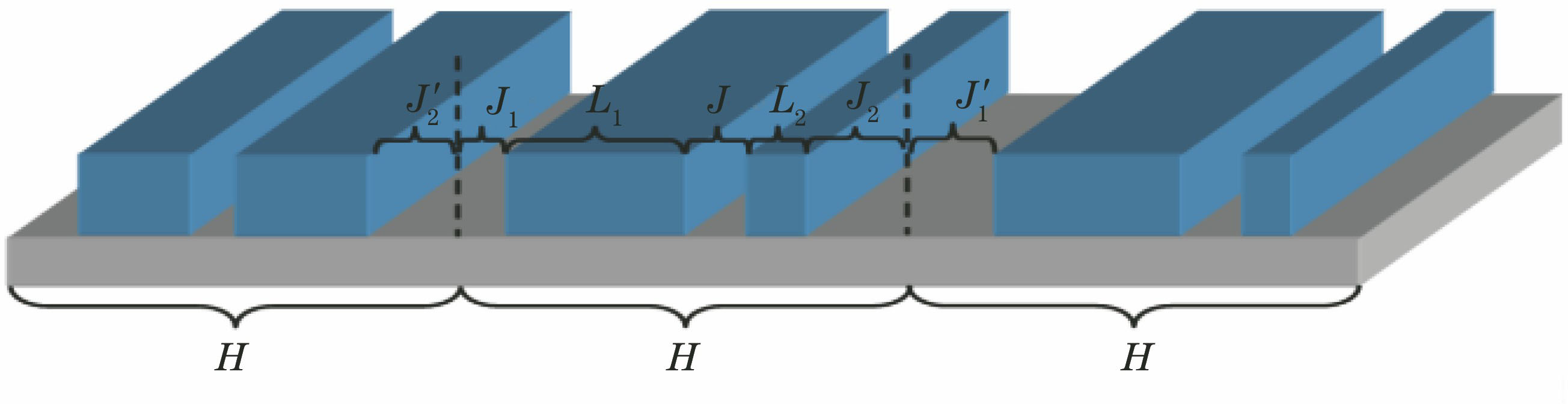
    Fig. 1. Grooved grating microstructure
    Phase modulation spectra of grooved grating microstructure with wavelengths of (a) 4.8 μm and (b) 10.6 μm
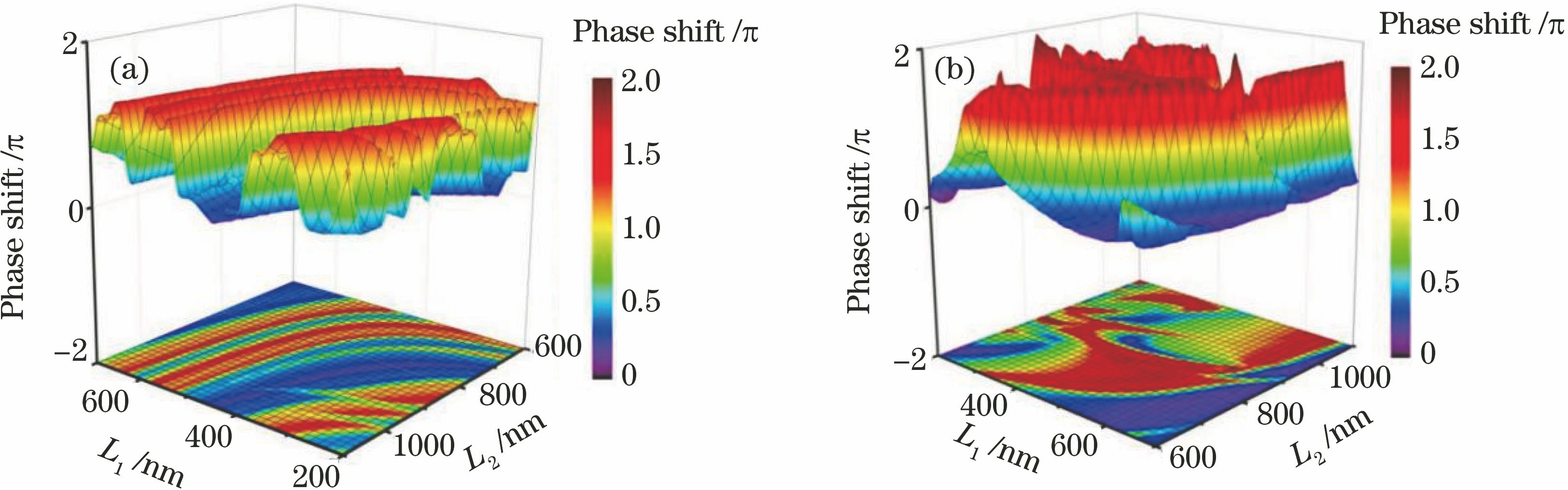
    Fig. 2. Phase modulation spectra of grooved grating microstructure with wavelengths of (a) 4.8 μm and (b) 10.6 μm
    Transmittance spectra of grooved grating microstructure with wavelengths of (a) 4.8 μm and (b) 10.6 μm
    Fig. 3. Transmittance spectra of grooved grating microstructure with wavelengths of (a) 4.8 μm and (b) 10.6 μm
    Distribution of phase retardation
    Fig. 4. Distribution of phase retardation
    Distribution of output light field
    Fig. 5. Distribution of output light field
    Chromatic aberration curves of ZnSe lens (a) without and (b) with grooved grating microstructure
    Fig. 6. Chromatic aberration curves of ZnSe lens (a) without and (b) with grooved grating microstructure
    Coating properties of ZEP520 photoresist
    Fig. 7. Coating properties of ZEP520 photoresist
    Testing and stitching of sub-field. (a) Home field offset of 1 mm×1 mm; (b) home field offset of 200 μm×200 μm
    Fig. 8. Testing and stitching of sub-field. (a) Home field offset of 1 mm×1 mm; (b) home field offset of 200 μm×200 μm
    Comparison for graphic quality at different exposure parameters. (a) Insufficient exposure; (b) sufficient exposure
    Fig. 9. Comparison for graphic quality at different exposure parameters. (a) Insufficient exposure; (b) sufficient exposure
    Surface morphology of sample from SEM
    Fig. 10. Surface morphology of sample from SEM
    Measured height of grooved grating microstructure
    Fig. 11. Measured height of grooved grating microstructure
    Infrared spectroscopy performance with wavelengths of (a) 4.8 μm and (b) 10.6 μm
    Fig. 12. Infrared spectroscopy performance with wavelengths of (a) 4.8 μm and (b) 10.6 μm
    NumberL1 /nmL2 /nmHeight ofsquare cylinder K /nmPhase mutationvalue at 10.6 μm /πPhase mutationvalue at 4.8 μm /π
    14008755000.250.22
    240010505000.500.17
    34009505000.750.05
    445010505001.000.12
    54007755001.250.07
    67009005001.500.23
    74009505001.750.16
    83508255002.000.08
    Table 1. Parameters of grooved grating microstructure unit
    ItemConvergent position atwavelength of 4.8 μm /mmConvergent position atwavelength of 10.6 μm /mmLongitudinal chromaticaberration /mm
    No sample01.131.13
    Adding sample0.240.580.34
    Table 2. Test data of longitudinal chromatic aberration
    Yanjun Sun, Jun Wang, Xuesong Ji, Li Wang, Yue Wang, Zhe Li. Simulation and Experiment of Grooved Grating Microstructure for Infrared Chromatic Aberration Correction[J]. Acta Optica Sinica, 2018, 38(7): 0724002
    Download Citation